US9025306B2 - Laminated capacitor having internal electrode connected to terminal electrode and internal electrode not connected to terminal electrode - Google Patents
Laminated capacitor having internal electrode connected to terminal electrode and internal electrode not connected to terminal electrode Download PDFInfo
- Publication number
- US9025306B2 US9025306B2 US13/958,919 US201313958919A US9025306B2 US 9025306 B2 US9025306 B2 US 9025306B2 US 201313958919 A US201313958919 A US 201313958919A US 9025306 B2 US9025306 B2 US 9025306B2
- Authority
- US
- United States
- Prior art keywords
- electrode
- internal
- terminal
- electrodes
- internal electrode
- Prior art date
- Legal status (The legal status is an assumption and is not a legal conclusion. Google has not performed a legal analysis and makes no representation as to the accuracy of the status listed.)
- Active, expires
Links
Images


Classifications
-
- H—ELECTRICITY
- H01—ELECTRIC ELEMENTS
- H01G—CAPACITORS; CAPACITORS, RECTIFIERS, DETECTORS, SWITCHING DEVICES, LIGHT-SENSITIVE OR TEMPERATURE-SENSITIVE DEVICES OF THE ELECTROLYTIC TYPE
- H01G4/00—Fixed capacitors; Processes of their manufacture
- H01G4/002—Details
- H01G4/005—Electrodes
-
- H—ELECTRICITY
- H01—ELECTRIC ELEMENTS
- H01G—CAPACITORS; CAPACITORS, RECTIFIERS, DETECTORS, SWITCHING DEVICES, LIGHT-SENSITIVE OR TEMPERATURE-SENSITIVE DEVICES OF THE ELECTROLYTIC TYPE
- H01G4/00—Fixed capacitors; Processes of their manufacture
- H01G4/38—Multiple capacitors, i.e. structural combinations of fixed capacitors
- H01G4/385—Single unit multiple capacitors, e.g. dual capacitor in one coil
Definitions
- the present invention relates to a laminated capacitor.
- the laminated capacitor described in Japanese Patent Application Laid-Open No. 2012-44148 includes a rectangular parallelepiped-shaped ceramic element assembly having first and second main surfaces extending along a length direction and width direction thereof, first and second side surfaces extending along a length direction and thickness direction thereof, and first and second end surfaces extending along a width direction and thickness direction thereof, first and second internal electrodes that are disposed in the element assembly, and terminal electrodes disposed over the end surfaces and main surfaces of the element assembly.
- This laminated capacitor is configured as a low-profile capacitor.
- An aspect of the present invention is a laminated capacitor including an element assembly having a pair of first and second end surfaces opposed to each other, a pair of first and second main surfaces extending so as to connect between a pair of the first and second end surfaces and opposed to each other, and a pair of first and second side surfaces extending so as to connect a pair of the first and second main surfaces and opposed to each other, first and second terminal electrodes disposed on both end portions of the element assembly, and each having a first electrode part located on at least the first main surface, first and second internal electrodes that are connected to corresponding terminal electrodes out of the first and second terminal electrodes, and disposed in the element assembly so as to be opposed to each other in a first direction in which the first main surface and the second main surface are opposed, and a third internal electrode that is disposed in the element assembly so as to be located, adjacent to the first main surface, outside in the first direction further than the first and second internal electrodes and be opposed to each of the first electrode parts of the first and second terminal electrodes, and not connected to the first
- This laminated capacitor has a first capacitance unit composed of the first internal electrode and the second internal electrode, a second capacitance unit composed of the first electrode part of the first terminal electrode and the third internal electrode, and a third capacitance unit composed of the first electrode part of the second terminal electrode and the third internal electrode.
- the interval between each of the first electrode parts of the first and second terminal electrodes and the third internal electrode is made smaller than the interval between the third internal electrode and the first internal electrode or the second internal electrode located adjacent to the third internal electrode, and in the second and third capacitance units consisting of the first and second terminal electrodes disposed on the main surface to serve as a mounting surface and the third internal electrode that is disposed at a position close to the terminal electrodes, the equivalent series inductance (hereinafter, referred to as ESL) is lowered.
- ESL equivalent series inductance
- the laminated capacitor when the first main surface is used as a mounting surface, because the third internal electrode is disposed closer to the first main surface, even if, for example, a crack occurs in the first and second terminal electrodes when the laminated capacitor is mounted, the influence on the first and second internal electrodes can be reduced, so that a short-circuit failure can be suppressed. Moreover, even if a crack occurs in the third internal electrode to disable either one of the second capacitance unit and the third capacitance unit from functioning, the other can secure the function, so that reliability such as insulation resistance can be improved.
- each of the first and second terminal electrodes has a second electrode part located on the second main surface
- the laminated capacitor includes a fourth internal electrode that is disposed in the element assembly so as to be located, adjacent to the second main surface, outside in the first direction further than the first and second internal electrodes and be opposed to each of the second electrode parts of the first and second terminal electrodes, and not connected to the first and second terminal electrodes
- the second capacitance unit is composed of the first and second electrode parts of the first terminal electrode and the third and fourth internal electrodes
- the third capacitance unit is composed of the first and second electrode parts of the second terminal electrode and the third and fourth internal electrodes
- an interval between each of the second electrode parts of the first and second terminal electrodes and the fourth internal electrode is smaller than an interval between the fourth internal electrode and the first internal electrode or the second internal electrode located adjacent to the fourth internal electrode.
- the ESL can be lowered.
- the element assembly has a dimension between the first and second main surfaces smaller than a dimension between the first and second end surfaces and a dimension between the first and second side surfaces.
- disposing only the third and fourth internal electrodes that serve as constituents of a capacitance unit and not disposing unnecessary internal electrodes that do not serve as constituents of a capacitance unit allows reliably forming a capacitance unit while simplifying the configuration.
- the separation distance g between the first terminal electrode and the second terminal electrode is shorter than a length in the third direction of each of the first and second terminal electrodes.
- the length of the first and second terminal electrodes is long, which allows securing an opposing area between the first and second terminal electrodes and the third and fourth internal electrodes, so that capacitance can be secured in the first and second terminal electrodes and the third and fourth internal electrodes.
- the separation distance g between the terminal electrodes to have opposite polarities is small, low ESL can be achieved.
- the first terminal electrode and the second terminal electrode may be further disposed on the first and second side surfaces
- the first internal electrode may have a first main electrode portion extending in a third direction in which the first end surface and the second end surface are opposed and a first lead-out electrode portion extending in a second direction in which the first side surface and the second side surface are opposed
- the second internal electrode may have a second main electrode portion extending in the third direction and a second lead-out electrode portion extending in the second direction.
- the interval t 1 between each of the first electrode parts and the third internal electrode and the interval t 2 between each of the second electrode parts and the fourth internal electrode may be 0.012 mm or more. According to this arrangement, a problem such that the third and fourth internal electrodes are exposed from the element assembly can be prevented.
- the separation distance g between the first terminal electrode and the second terminal electrode may be 0.15 mm or more. According to this arrangement, a mounting failure can be suppressed when the laminated capacitor is mounted.
- low impedance can be achieved over a wide band.
- FIG. 1 is a perspective view showing a laminated capacitor according to an embodiment.
- FIG. 2 is a view showing a sectional configuration of the laminated capacitor.
- FIG. 3 is an exploded perspective view showing a configuration of an element assembly.
- FIG. 4 is a sectional view showing internal electrodes.
- FIG. 5 is a graph showing a relationship between the dimensions of respective portions and ESL.
- FIG. 6 is a circuit diagram of the laminated capacitor.
- FIG. 7 is a sectional view showing a mounting structure of the laminated capacitor.
- FIG. 8 is a perspective view showing a laminated capacitor according to another embodiment.
- FIG. 1 is a perspective view showing a laminated capacitor according to an embodiment.
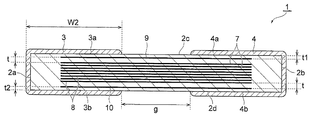
- FIG. 2 is a view showing a sectional configuration of the laminated capacitor.
- FIG. 3 is an exploded perspective view showing a configuration of an element assembly.
- the laminated capacitor 1 is constructed including an element assembly 2 formed in a substantially rectangular parallelepiped shape, internal electrodes (a first internal electrode, a second internal electrode, a third internal electrode, a fourth internal electrode) 7 , 8 , 9 , 10 disposed in the element assembly 2 , and first and second terminal electrodes 3 , 4 formed on both end surface sides of the element assembly 2 .
- the laminated capacitor 1 is set to, for example, a length L of approximately 0.95 mm to 1.05 mm, a width W 1 of approximately 0.45 mm to 0.55 mm, and a height T of approximately 0.09 mm to 0.22 mm.
- the laminated capacitor 1 is configured as a so-called low-profile type capacitor.
- the element assembly 2 has a pair of first and second end surfaces 2 a , 2 b facing in the longitudinal direction of the element assembly 2 to be parallel to each other, a pair of first and second main surfaces 2 c , 2 d extending so as to connect between the first and second end surfaces 2 a , 2 b and opposed to each other, and a pair of first and second side surfaces 2 e , 2 f extending so as to connect the first and second main surfaces 2 c , 2 d and opposed to each other.
- the element assembly 2 has a dimension between the first and second main surfaces 2 c , 2 d that is smaller than a dimension between the first and second end surfaces 2 a , 2 b and a dimension between the first and second side surfaces 2 e , 2 f.
- the element assembly 2 is formed, as shown in FIG. 2 and FIG. 3 , as a lamination for which a plurality of rectangular plate-shaped dielectric layers 6 and pluralities of internal electrodes 7 and internal electrodes 8 are laminated.
- the internal electrodes 7 and the internal electrodes 8 are disposed in the element assembly 2 one each for each layer along a lamination direction of the dielectric layers 6 , that is, a first direction in which the first main surface 2 c and the second main surface 2 d of the element assembly 2 are opposed (hereinafter, simply referred to as a first direction).
- the internal electrode 7 and the internal electrode 8 are disposed opposed so as to sandwich at least one dielectric layer 6 .
- the plurality of dielectric layers 6 are integrated to such an extent that boundaries with each other are not visible.
- the first terminal electrode 3 is disposed so as to cover the first end surface 2 a , a part of each edge portion of the first and second main surfaces 2 c , 2 d , and first and second side surfaces 2 e , 2 f . That is, the terminal electrode 3 is disposed over the first end surface 2 a , the first and second main surfaces 2 c , 2 d , and the first and second side surfaces 2 e , 2 f .
- the first terminal electrode 3 has a first electrode part 3 a located on the first main surface 2 c and a second electrode part 3 b located on the second main surface 2 d.
- the second terminal electrode 4 is disposed so as to cover the second end surface 2 b , a part of each edge portion of the first and second main surfaces 2 c , 2 d , and the first and second side surfaces 2 e , 2 f . That is, the terminal electrode 4 is disposed over the second end surface 2 b , the first and second main surfaces 2 c , 2 d , and the first and second side surfaces 2 e , 2 f .
- the second terminal electrode 4 has a first electrode part 4 a located on the first main surface 2 c and a second electrode part 4 b located on the second main surface 2 d . As shown in FIG. 2 , the separation distance g between the first terminal electrode 3 and the second terminal electrode 4 is smaller than the length (width) W 2 in the opposing direction of the first and second end surfaces 2 a , 2 b of the terminal electrodes 3 , 4 .
- the internal electrode 7 has a first main electrode portion 7 a extending in a third direction in which the first end surface 2 a and the second end surface 2 b are opposed (hereinafter, simply referred to as a third direction) and first lead-out electrode portions 7 b , 7 c extending in a second direction in which the first side surface 2 e and the second side surface 2 f are opposed (hereinafter, simply referred to as a second direction).
- the first main electrode portion 7 a shows a substantially rectangular shape.
- Each of the first lead-out electrode portions 7 b , 7 c is led out from one side of the first main electrode portion 7 a , and is exposed to each of the first and second side surfaces 2 e , 2 f to be connected to the first terminal electrode 3 . Accordingly, the internal electrode 7 and the terminal electrode 3 are electrically connected.
- the internal electrode 8 has a second main electrode portion 8 a extending in the third direction and second lead-out electrode portions 8 b , 8 c extending in the second direction.
- the second main electrode portion 8 a shows a substantially rectangular shape.
- Each of the second lead-out electrode portions 8 b , 8 e is led out from one side of the second main electrode portion 8 a , and is exposed to each of the first and second side surfaces 2 e , 2 f to be connected to the second terminal electrode 4 .
- the internal electrode 8 and the terminal electrode 4 are electrically connected.
- FIG. 4 is a sectional view showing internal electrodes.
- an internal electrode 9 and an internal electrode 10 in the element assembly 2 there is further disposed an internal electrode 9 and an internal electrode 10 in the element assembly 2 .
- the internal electrode 9 shows a substantially rectangular shape, and is located outside in the first direction further than the internal electrodes 7 , 8 and closer to the main surface 2 c .
- the internal electrode 9 is disposed opposed to the first electrode part 3 a of the first terminal electrode 3 and the first electrode part 4 a of the second terminal electrode 4 .
- the internal electrode 9 is an electrode that is not electrically connected to the first and second terminal electrodes 3 , 4 , and is a floating electrode.
- the internal electrode 10 shows a substantially rectangular shape, and is located on the outside in the first direction further than the internal electrodes 7 , 8 and closer to the main surface 2 d .
- the internal electrode 10 is disposed opposed to the second electrode part 3 b of the first terminal electrode 3 and the second electrode part 4 b of the second terminal electrode 4 .
- the internal electrode 10 is an electrode that is not electrically connected to the first and second terminal electrodes 3 , 4 , and is a floating electrode.
- the internal electrodes 9 , 10 are disposed one each in the element assembly 2 .
- the interval t 1 between each of the first electrode parts 3 a , 4 a of the first and second terminal electrodes 3 , 4 and the internal electrode 9 and the interval t 2 between each of the second electrode parts 3 b , 4 b of the first and second terminal electrodes 3 , 4 and the internal electrode 10 are smaller than the interval t between the internal electrode 9 and the internal electrode 7 located adjacent to the internal electrode 9 and the interval t between the internal electrode 10 and the internal electrode 8 located adjacent to the internal electrode 10 .
- t 1 represents the interval between the internal electrode 9 and the first electrode parts 3 a , 4 a of the first and second terminal electrodes 3 , 4 (refer to FIG. 2 )
- t 2 represents the interval between the internal electrode 10 and the second electrode parts 3 b , 4 b of the first and second terminal electrodes 3 , 4
- g represents separation distance between the first terminal electrode 3 and the second terminal electrode 4 in the third direction (refer to FIG.
- the separation distance g is a distance between positions where the first terminal electrode 3 and the second terminal electrode 4 are closest to each other, connected by a straight line along the opposing direction of the first and second end surfaces 2 a , 2 b.
- FIG. 5 is a graph showing a relationship between the dimensions of respective portions and ESL.
- the horizontal axis shows numerical values of (t 1 , t 2 ⁇ d)/w
- the longitudinal axis shows ESL [pH].
- the above-described expressions (1), (2) are satisfied, that is, when the value of each of (t 1 ⁇ g)/w and (t 2 ⁇ g)/w is 0.025 or less, low ESL can be achieved.
- the interval t 1 between the internal electrode 9 and the first electrode parts 3 a , 4 a of the first and second terminal electrodes 3 , 4 and the interval t 2 between the internal electrode 10 and the second electrode parts 3 b , 4 b of the first and second terminal electrodes 3 , 4 are 0.012 mm or more (t 1 , t 2 ⁇ 0.012 mm). If these intervals t 1 , t 2 are smaller than 0.012 mm, the internal electrodes 9 , 10 are likely to be exposed from the element assembly 2 . Therefore, by setting the intervals t 1 , t 2 to 0.012 mm or more, a problem such that the internal electrodes 9 , 10 are exposed from the element assembly 2 can be prevented.
- the separation distance g between the first terminal electrode 3 and the second terminal electrode 4 is 0.15 mm or more (g ⁇ 0.15 mm). If this separation distance g is smaller than 0.15 mm, a mounting failure is likely to occur when the laminated capacitor 1 is mounted (for example, a short circuit between the first terminal electrode 3 and the second terminal electrode 4 when being solder-mounted). Therefore, by setting the separation distance g to 0.15 mm or more, a mounting failure of the laminated capacitor 1 can be suppressed.
- FIG. 6 is a circuit diagram of the laminated capacitor.
- the element assembly 2 of the laminated capacitor 1 has a first capacitor unit (a first capacitance unit) C 1 consisting of the internal electrode 7 and the internal electrode 8 , a second capacitor unit (a second capacitance unit) C 2 consisting of the terminal electrode 3 and the internal electrodes 9 , 10 , and a third capacitor unit (a third capacitance unit) C 3 consisting of the terminal electrode 4 and the internal electrodes 9 , 10 .
- a capacitor C 21 composed of the first electrode part 3 a of the terminal electrode 3 and the internal electrode 9 and a capacitor C 22 composed of the second electrode part 3 b of the terminal electrode 3 and the internal electrode 10 are connected in parallel.
- a capacitor C 31 composed of the first electrode part 4 a of the terminal electrode 4 and the internal electrode 9 and a capacitor C 32 composed of the second electrode part 4 b of the terminal electrode 4 and the internal electrode 10 are connected in parallel.
- the capacitor C 21 and the capacitor C 31 are connected in series, and the capacitor C 22 and the capacitor C 32 are connected in series.
- the second capacitor unit C 2 and the third capacitor unit C 3 are connected in series to form a series circuit. Moreover, the first capacitor unit C 1 and the second capacitor unit C 2 and the third capacitor unit C 3 are connected in parallel to form a parallel circuit.
- FIG. 7 is a sectional view showing a mounting structure of the laminated capacitor.
- the laminated capacitor 1 is mounted by being embedded in a substrate 20 .
- the substrate 20 is composed of a plurality of laminated insulating resin sheets 22 .
- the laminated capacitor 1 is disposed in the substrate 20 , and embedded inside the substrate 20 by being filled with a resin 23 .
- the laminated capacitor 1 is electrically connected by via conductors 26 , 27 with electrodes 24 , 25 formed on the surface of the substrate 20 .
- the via conductor 26 is connected physically and electrically.
- the connection between the first terminal electrode 3 and the via conductor 26 can be reliably performed. Accordingly, the first terminal electrode 3 and the electrode 24 are electrically connected.
- the via conductor 27 is connected physically and electrically.
- the connection between the second terminal electrode 4 and the via conductor 27 can be reliably performed. Accordingly, the second terminal electrode 4 and the electrode 25 are electrically connected.
- the element assembly 2 has a first capacitor unit C 1 , a second capacitor unit C 2 , and a third capacitor unit C 3 , and the first to third capacitor units C 1 to C 3 are connected in parallel.
- the plurality of capacitor units C 1 to C 3 being connected in series and parallel, low impedance in a wide band can be achieved in the low-profile type laminated capacitor 1 .
- the interval t 1 between each of the first electrode parts 3 a , 4 a of the first and second terminal electrodes 3 , 4 and the internal electrode 9 and the interval t 2 between each of the second electrode parts 3 b , 4 b of the first and second terminal electrodes 3 , 4 and the internal electrode 10 are smaller than the interval t between the internal electrode 9 and the internal electrode 7 located adjacent to the internal electrode 9 and the interval t between the internal electrode 10 and the internal electrode 8 located adjacent to the internal electrode 10 .
- the ESL is lowered.
- a lowered impedance can be favorably realized over a wide band.
- the internal electrodes 9 , 10 are disposed closer to the first and second main surfaces 2 c , 2 d , respectively, either of which serves as a mounting surface, even if, for example, a crack of the element assembly 2 occurs when the laminated capacitor 1 is mounted, the influence on the internal electrodes 7 , 8 can be reduced, so that a short-circuit failure can be suppressed.
- the other can secure the function, so that reliability such as insulation resistance can be improved.
- the interval t 1 , t 2 between the internal electrode 9 , 10 and the terminal electrodes 3 , 4 on the main surface 2 c , 2 d , the separation distance g between the first terminal electrode 3 and the second terminal electrode 4 in the opposing direction of the first and second end surfaces 2 a , 2 b , and the width dimension w in the opposing direction of the first and second side surfaces 2 e , 2 f of the internal electrodes 9 , 10 satisfy the relationship of: ( t 1 ⁇ g )/ w ⁇ 0.025 (mm) (1) ( t 2 ⁇ g )/ w ⁇ 0.025 (mm) (2)
- the ESL can be lowered. Accordingly, low impedance in a wide band can be more favorably achieved.
- the separation distance g between the first terminal electrode 3 and the second terminal electrode 4 is shorter than the length (width) W 2 in the third direction of the first and second terminal electrodes 3 , 4 .
- the length of the first and second terminal electrodes 3 , 4 is long, which allows securing an opposing area between the first and second terminal electrodes 3 , 4 and the internal electrodes 9 , 10 , so that capacitance can be secured.
- the separation distance g between the first terminal electrode 3 and the second terminal electrode 4 to have opposite polarities is small, the ESL can be lowered.
- the internal electrodes 9 , 10 are disposed one each in the element assembly 2 .
- solely disposing a floating electrode that serves as a constituent of a capacitor unit allows reliably forming a capacitor unit while simplifying the configuration.
- FIG. 8 is a perspective view showing a laminated capacitor according to another embodiment.
- the laminated capacitor 1 A includes first and second terminal electrodes 3 A, 4 A.
- the first terminal electrode 3 A is disposed on the first main surface 2 c , 2 d and the first and second side surfaces 2 e , 2 f of the element assembly 2 . In other words, the first terminal electrode 3 A is not disposed on the first end surface 2 a .
- the second terminal electrode 4 A is disposed on the first main surface 2 c , 2 d and the first and second side surfaces 2 e , 2 f of the element assembly 2 . In other words, the second terminal electrode 4 A is not disposed on the second end surface 2 b.
- the low-profile type laminated capacitor 1 , 1 A but the laminated capacitor 1 , 1 A are not necessarily a low-profile type.
- the shapes of the internal electrodes 7 , 8 may be other shapes.
Landscapes
- Engineering & Computer Science (AREA)
- Power Engineering (AREA)
- Manufacturing & Machinery (AREA)
- Microelectronics & Electronic Packaging (AREA)
- Ceramic Capacitors (AREA)
- Fixed Capacitors And Capacitor Manufacturing Machines (AREA)
Abstract
Description
(t1×g)/w≦0.025 (mm)
(t2×g)/w≦0.025 (mm).
Thus, in the laminated capacitor, as a result of satisfying the relationship of (t1×g)/w≦0.025 (mm) and (t2×g)/w≦0.025 (mm), the ESL can be lowered.
(t1×g)/w≦0.025 (mm) (1)
(t2×g)/w≦0.025 (mm) (2)
In the above-described expressions (1), (2), t1 represents the interval between the
(t1×g)/w≦0.025 (mm) (1)
(t2×g)/w≦0.025 (mm) (2)
Thus, as a result of setting the dimensions of the respective portions so as to satisfy the expressions (1), (2), the ESL can be lowered. Accordingly, low impedance in a wide band can be more favorably achieved.
Claims (7)
(t1×g)/w≦0.025 (mm)
(t2×g)/w≦0.025 (mm)
Applications Claiming Priority (2)
| Application Number | Priority Date | Filing Date | Title |
|---|---|---|---|
| JP2012178607A JP6079040B2 (en) | 2012-08-10 | 2012-08-10 | Multilayer capacitor |
| JP2012-178607 | 2012-08-10 |
Publications (2)
| Publication Number | Publication Date |
|---|---|
| US20140043719A1 US20140043719A1 (en) | 2014-02-13 |
| US9025306B2 true US9025306B2 (en) | 2015-05-05 |
Family
ID=50066022
Family Applications (1)
| Application Number | Title | Priority Date | Filing Date |
|---|---|---|---|
| US13/958,919 Active 2033-09-05 US9025306B2 (en) | 2012-08-10 | 2013-08-05 | Laminated capacitor having internal electrode connected to terminal electrode and internal electrode not connected to terminal electrode |
Country Status (2)
| Country | Link |
|---|---|
| US (1) | US9025306B2 (en) |
| JP (1) | JP6079040B2 (en) |
Cited By (2)
| Publication number | Priority date | Publication date | Assignee | Title |
|---|---|---|---|---|
| US20160042865A1 (en) * | 2014-08-05 | 2016-02-11 | Samsung Electro-Mechanics Co., Ltd. | Multi-layer ceramic capacitor |
| US10607777B2 (en) | 2017-02-06 | 2020-03-31 | Avx Corporation | Integrated capacitor filter and integrated capacitor filter with varistor function |
Families Citing this family (12)
| Publication number | Priority date | Publication date | Assignee | Title |
|---|---|---|---|---|
| JP5811114B2 (en) * | 2013-02-28 | 2015-11-11 | 株式会社村田製作所 | Electronic components |
| KR102057909B1 (en) * | 2013-06-14 | 2019-12-20 | 삼성전기주식회사 | Multi-layered ceramic capacitor and mounting circuit of multi-layered ceramic capacitor |
| KR101452126B1 (en) * | 2013-08-08 | 2014-10-16 | 삼성전기주식회사 | Embedded multilayer ceramic electronic part and print circuit board having embedded multilayer ceramic electronic part |
| US9396879B2 (en) | 2013-10-29 | 2016-07-19 | Samsung Electro-Mechanics Co., Ltd. | Multilayer ceramic capacitor and board having the same |
| JP2015111651A (en) * | 2013-10-29 | 2015-06-18 | 株式会社村田製作所 | Multilayer ceramic capacitor |
| KR101641574B1 (en) * | 2014-02-03 | 2016-07-22 | 삼성전기주식회사 | Embedded multilayer ceramic electronic component, manufacturing method thereof and print circuit board having embedded multilayer ceramic electronic component |
| JP2016040816A (en) * | 2014-08-13 | 2016-03-24 | 株式会社村田製作所 | Multilayer ceramic capacitor, multilayer ceramic capacitor couple including the same, and multilayer ceramic capacitor assembly |
| US20160055976A1 (en) * | 2014-08-25 | 2016-02-25 | Qualcomm Incorporated | Package substrates including embedded capacitors |
| KR102048101B1 (en) | 2014-11-07 | 2019-11-22 | 삼성전기주식회사 | Multi-layered chip component and board for mounting the same |
| JP6867745B2 (en) * | 2015-02-13 | 2021-05-12 | Tdk株式会社 | Multilayer capacitor and mounting structure of multilayer capacitor |
| JP7156914B2 (en) * | 2018-11-13 | 2022-10-19 | 株式会社村田製作所 | Laminated ceramic capacitor and method for manufacturing the same |
| KR102785608B1 (en) * | 2023-06-22 | 2025-03-25 | (주)모던텍 | Charging device having a display unit for an electric vehicle charging cable |
Citations (7)
| Publication number | Priority date | Publication date | Assignee | Title |
|---|---|---|---|---|
| JPH1126295A (en) * | 1997-06-30 | 1999-01-29 | Taiyo Yuden Co Ltd | Multilayered chip component |
| US6661640B2 (en) * | 2001-08-03 | 2003-12-09 | Tdk Corporation | Multilayer ceramic electronic device |
| US7307829B1 (en) * | 2002-05-17 | 2007-12-11 | Daniel Devoe | Integrated broadband ceramic capacitor array |
| US7394646B2 (en) * | 2005-03-28 | 2008-07-01 | Tdk Corporation | Laminated ceramic electronic component |
| US20110102969A1 (en) * | 2009-11-05 | 2011-05-05 | Tdk Corporation | Multilayer capacitor, mounting structure thereof, and method of manufacturing same |
| US20120019978A1 (en) * | 2010-07-21 | 2012-01-26 | Murata Manufacturing Co., Ltd. | Ceramic electronic component |
| US20120112855A1 (en) * | 2009-07-28 | 2012-05-10 | Sony Corporation | Capacitance element and resonance circuit |
Family Cites Families (3)
| Publication number | Priority date | Publication date | Assignee | Title |
|---|---|---|---|---|
| JPH0244318U (en) * | 1988-09-20 | 1990-03-27 | ||
| JP5589891B2 (en) * | 2010-05-27 | 2014-09-17 | 株式会社村田製作所 | Ceramic electronic component and method for manufacturing the same |
| JP5699819B2 (en) * | 2010-07-21 | 2015-04-15 | 株式会社村田製作所 | Ceramic electronic components |
-
2012
- 2012-08-10 JP JP2012178607A patent/JP6079040B2/en active Active
-
2013
- 2013-08-05 US US13/958,919 patent/US9025306B2/en active Active
Patent Citations (8)
| Publication number | Priority date | Publication date | Assignee | Title |
|---|---|---|---|---|
| JPH1126295A (en) * | 1997-06-30 | 1999-01-29 | Taiyo Yuden Co Ltd | Multilayered chip component |
| US6661640B2 (en) * | 2001-08-03 | 2003-12-09 | Tdk Corporation | Multilayer ceramic electronic device |
| US7307829B1 (en) * | 2002-05-17 | 2007-12-11 | Daniel Devoe | Integrated broadband ceramic capacitor array |
| US7394646B2 (en) * | 2005-03-28 | 2008-07-01 | Tdk Corporation | Laminated ceramic electronic component |
| US20120112855A1 (en) * | 2009-07-28 | 2012-05-10 | Sony Corporation | Capacitance element and resonance circuit |
| US20110102969A1 (en) * | 2009-11-05 | 2011-05-05 | Tdk Corporation | Multilayer capacitor, mounting structure thereof, and method of manufacturing same |
| US20120019978A1 (en) * | 2010-07-21 | 2012-01-26 | Murata Manufacturing Co., Ltd. | Ceramic electronic component |
| JP2012044148A (en) | 2010-07-21 | 2012-03-01 | Murata Mfg Co Ltd | Ceramic electronic component |
Cited By (3)
| Publication number | Priority date | Publication date | Assignee | Title |
|---|---|---|---|---|
| US20160042865A1 (en) * | 2014-08-05 | 2016-02-11 | Samsung Electro-Mechanics Co., Ltd. | Multi-layer ceramic capacitor |
| US10607777B2 (en) | 2017-02-06 | 2020-03-31 | Avx Corporation | Integrated capacitor filter and integrated capacitor filter with varistor function |
| US11295895B2 (en) | 2017-02-06 | 2022-04-05 | KYOCERA AVX Components Corporation | Integrated capacitor filter and integrated capacitor filter with varistor function |
Also Published As
| Publication number | Publication date |
|---|---|
| US20140043719A1 (en) | 2014-02-13 |
| JP6079040B2 (en) | 2017-02-15 |
| JP2014036214A (en) | 2014-02-24 |
Similar Documents
| Publication | Publication Date | Title |
|---|---|---|
| US9025306B2 (en) | Laminated capacitor having internal electrode connected to terminal electrode and internal electrode not connected to terminal electrode | |
| US8526162B2 (en) | Feedthrough multilayer capacitor | |
| US8988180B2 (en) | Multilayer coil component | |
| US9431174B2 (en) | Multilayer capacitor | |
| US8659871B2 (en) | Multilayer capacitor having reduced equivalent series inductance | |
| US8493710B2 (en) | Multilayer capacitor with improved adhesiveness between the layers | |
| CN108364785B (en) | Multilayer capacitor and electronic component device | |
| JP6464614B2 (en) | Multilayer coil parts | |
| US7808768B2 (en) | Multilayer capacitor | |
| US8068330B2 (en) | Multilayer capacitor | |
| US8189321B2 (en) | Multilayer capacitor | |
| JP4428446B2 (en) | Multilayer capacitor | |
| JP6201477B2 (en) | Multilayer capacitor | |
| US7265964B1 (en) | Multilayer feedthrough capacitor array | |
| KR102148830B1 (en) | Electronic component | |
| JP5131263B2 (en) | Multilayer capacitor | |
| US10546694B2 (en) | Multilayer capacitor | |
| JP6115276B2 (en) | Multilayer capacitor | |
| JP5131264B2 (en) | Multilayer capacitor | |
| CN111261366B (en) | Laminated coil component | |
| JP6142652B2 (en) | Multilayer capacitor |
Legal Events
| Date | Code | Title | Description |
|---|---|---|---|
| AS | Assignment |
Owner name: TDK CORPORATION, JAPAN Free format text: ASSIGNMENT OF ASSIGNORS INTEREST;ASSIGNOR:TOGASHI, MASAAKI;REEL/FRAME:031032/0044 Effective date: 20130726 |
|
| STCF | Information on status: patent grant |
Free format text: PATENTED CASE |
|
| FEPP | Fee payment procedure |
Free format text: PAYOR NUMBER ASSIGNED (ORIGINAL EVENT CODE: ASPN); ENTITY STATUS OF PATENT OWNER: LARGE ENTITY |
|
| MAFP | Maintenance fee payment |
Free format text: PAYMENT OF MAINTENANCE FEE, 4TH YEAR, LARGE ENTITY (ORIGINAL EVENT CODE: M1551); ENTITY STATUS OF PATENT OWNER: LARGE ENTITY Year of fee payment: 4 |
|
| MAFP | Maintenance fee payment |
Free format text: PAYMENT OF MAINTENANCE FEE, 8TH YEAR, LARGE ENTITY (ORIGINAL EVENT CODE: M1552); ENTITY STATUS OF PATENT OWNER: LARGE ENTITY Year of fee payment: 8 |