US9018634B2 - Semiconductor device - Google Patents
Semiconductor device Download PDFInfo
- Publication number
- US9018634B2 US9018634B2 US14/165,405 US201414165405A US9018634B2 US 9018634 B2 US9018634 B2 US 9018634B2 US 201414165405 A US201414165405 A US 201414165405A US 9018634 B2 US9018634 B2 US 9018634B2
- Authority
- US
- United States
- Prior art keywords
- semiconductor layer
- nitride semiconductor
- field effect
- effect transistor
- type
- Prior art date
- Legal status (The legal status is an assumption and is not a legal conclusion. Google has not performed a legal analysis and makes no representation as to the accuracy of the status listed.)
- Active
Links
Images


Classifications
-
- H01L29/778—
-
- H—ELECTRICITY
- H10—SEMICONDUCTOR DEVICES; ELECTRIC SOLID-STATE DEVICES NOT OTHERWISE PROVIDED FOR
- H10D—INORGANIC ELECTRIC SEMICONDUCTOR DEVICES
- H10D62/00—Semiconductor bodies, or regions thereof, of devices having potential barriers
- H10D62/10—Shapes, relative sizes or dispositions of the regions of the semiconductor bodies; Shapes of the semiconductor bodies
- H10D62/102—Constructional design considerations for preventing surface leakage or controlling electric field concentration
- H10D62/103—Constructional design considerations for preventing surface leakage or controlling electric field concentration for increasing or controlling the breakdown voltage of reverse-biased devices
- H10D62/105—Constructional design considerations for preventing surface leakage or controlling electric field concentration for increasing or controlling the breakdown voltage of reverse-biased devices by having particular doping profiles, shapes or arrangements of PN junctions; by having supplementary regions, e.g. junction termination extension [JTE]
- H10D62/106—Constructional design considerations for preventing surface leakage or controlling electric field concentration for increasing or controlling the breakdown voltage of reverse-biased devices by having particular doping profiles, shapes or arrangements of PN junctions; by having supplementary regions, e.g. junction termination extension [JTE] having supplementary regions doped oppositely to or in rectifying contact with regions of the semiconductor bodies, e.g. guard rings with PN or Schottky junctions
-
- H—ELECTRICITY
- H10—SEMICONDUCTOR DEVICES; ELECTRIC SOLID-STATE DEVICES NOT OTHERWISE PROVIDED FOR
- H10D—INORGANIC ELECTRIC SEMICONDUCTOR DEVICES
- H10D30/00—Field-effect transistors [FET]
- H10D30/40—FETs having zero-dimensional [0D], one-dimensional [1D] or two-dimensional [2D] charge carrier gas channels
- H10D30/47—FETs having zero-dimensional [0D], one-dimensional [1D] or two-dimensional [2D] charge carrier gas channels having two-dimensional [2D] charge carrier gas channels, e.g. nanoribbon FETs or high electron mobility transistors [HEMT]
-
- H01L29/2003—
-
- H01L29/41725—
-
- H01L29/66462—
-
- H01L29/7787—
-
- H—ELECTRICITY
- H10—SEMICONDUCTOR DEVICES; ELECTRIC SOLID-STATE DEVICES NOT OTHERWISE PROVIDED FOR
- H10D—INORGANIC ELECTRIC SEMICONDUCTOR DEVICES
- H10D30/00—Field-effect transistors [FET]
- H10D30/01—Manufacture or treatment
- H10D30/015—Manufacture or treatment of FETs having heterojunction interface channels or heterojunction gate electrodes, e.g. HEMT
-
- H—ELECTRICITY
- H10—SEMICONDUCTOR DEVICES; ELECTRIC SOLID-STATE DEVICES NOT OTHERWISE PROVIDED FOR
- H10D—INORGANIC ELECTRIC SEMICONDUCTOR DEVICES
- H10D30/00—Field-effect transistors [FET]
- H10D30/40—FETs having zero-dimensional [0D], one-dimensional [1D] or two-dimensional [2D] charge carrier gas channels
- H10D30/47—FETs having zero-dimensional [0D], one-dimensional [1D] or two-dimensional [2D] charge carrier gas channels having two-dimensional [2D] charge carrier gas channels, e.g. nanoribbon FETs or high electron mobility transistors [HEMT]
- H10D30/471—High electron mobility transistors [HEMT] or high hole mobility transistors [HHMT]
- H10D30/475—High electron mobility transistors [HEMT] or high hole mobility transistors [HHMT] having wider bandgap layer formed on top of lower bandgap active layer, e.g. undoped barrier HEMTs such as i-AlGaN/GaN HEMTs
- H10D30/4755—High electron mobility transistors [HEMT] or high hole mobility transistors [HHMT] having wider bandgap layer formed on top of lower bandgap active layer, e.g. undoped barrier HEMTs such as i-AlGaN/GaN HEMTs having wide bandgap charge-carrier supplying layers, e.g. modulation doped HEMTs such as n-AlGaAs/GaAs HEMTs
-
- H—ELECTRICITY
- H10—SEMICONDUCTOR DEVICES; ELECTRIC SOLID-STATE DEVICES NOT OTHERWISE PROVIDED FOR
- H10D—INORGANIC ELECTRIC SEMICONDUCTOR DEVICES
- H10D64/00—Electrodes of devices having potential barriers
- H10D64/20—Electrodes characterised by their shapes, relative sizes or dispositions
- H10D64/23—Electrodes carrying the current to be rectified, amplified, oscillated or switched, e.g. sources, drains, anodes or cathodes
- H10D64/251—Source or drain electrodes for field-effect devices
-
- H—ELECTRICITY
- H10—SEMICONDUCTOR DEVICES; ELECTRIC SOLID-STATE DEVICES NOT OTHERWISE PROVIDED FOR
- H10D—INORGANIC ELECTRIC SEMICONDUCTOR DEVICES
- H10D62/00—Semiconductor bodies, or regions thereof, of devices having potential barriers
- H10D62/80—Semiconductor bodies, or regions thereof, of devices having potential barriers characterised by the materials
- H10D62/85—Semiconductor bodies, or regions thereof, of devices having potential barriers characterised by the materials being Group III-V materials, e.g. GaAs
- H10D62/8503—Nitride Group III-V materials, e.g. AlN or GaN
Definitions
- the present disclosure relates to nitride field effect transistors applicable to power transistors used for power supply circuits of consumer appliances such as air conditioners and light controllers, for example.
- Nitride semiconductors are large in bandgap, breakdown electric field, and electron saturated drift velocity compared with Si, GaAs, etc.
- two-dimensional electron gas also expressed as “2DEG”
- 2DEG two-dimensional electron gas
- HEMT high electron mobility transistor
- FIG. 12 is a cross-sectional view showing a semiconductor device including a conventional HEMT having an AlGaN/GaN heterostructure.
- a low-temperature AlN buffer layer 2 an undoped GaN layer 3 , and an undoped AlGaN layer 4 are formed in this order on an Si Substrate 1 , and a source electrode 5 and a drain electrode 6 are formed to be in contact with the undoped AlGaN layer 4 .
- a gate electrode 7 is formed between the source electrode 5 and the drain electrode 6 .
- two-dimensional electron gas is generated near the interface between the undoped GaN layer 3 and the undoped AlGaN layer 4 due to spontaneous polarization and piezoelectric polarization, and this gas is used as a carrier.
- a voltage is applied between the source and the drain, electrons in the channel flow from the source electrode 5 toward the drain electrode 6 .
- the drain current can be controlled.
- the current collapse refers to a phenomenon that, once a high voltage is applied to the drain of a field effect transistor in its off state, the on resistance at the time when the field effect transistor is next switched to its on state will increase.
- FIG. 2 is a cross-sectional view of the semiconductor device including the general HEMT shown in FIG. 12 in its off state.
- a depletion layer 12 as illustrated is generated when the HEMT as the field effect transistor is off.
- a high electric field is generated in a region 13 on the drain terminal-side of the depletion layer 12 , and electrons are trapped in this region.
- the trapped electrons When the trapped electrons are present near the two-dimensional electron gas, they bring about an effect similar to that brought about when a negative-bias gate voltage is applied. Thus, the concentration of the two-dimensional electron gas near the trapped electrons decreases, resulting in increase in on-voltage and decrease in the current at the time when the device is turned on. This is the mechanism of development of current collapse.
- occurrence of current collapse can be prevented or reduced in a field effect transistor using nitride semiconductors.
- a semiconductor device of an example of the present disclosure includes a field effect transistor that has a first nitride semiconductor layer formed on a substrate, a second nitride semiconductor layer larger in bandgap than the first nitride semiconductor layer formed on the first nitride semiconductor layer, a gate electrode formed on the second nitride semiconductor layer, and a source electrode and a drain electrode formed to sandwich the gate electrode each being in contact with at least the second nitride semiconductor layer, and uses two-dimensional electron gas formed at an interface between the first nitride semiconductor layer and the second nitride semiconductor layer as a channel.
- the field effect transistor further has a p-type nitride semiconductor layer formed on the second nitride semiconductor layer at a position between the gate electrode and the drain electrode and electrically connected to the drain electrode.
- a field effect transistor in its off state in which a high electric field is applied to a region of the first nitride semiconductor layer located between the source and the drain, a number of electrons are left behind in the region after the transistor is switched to its on state.
- holes can be injected into the first nitride semiconductor layer from the p-type nitride semiconductor layer formed between the gate electrode and the drain electrode when the field effect transistor is in the on state.
- the remaining electrons in the first nitride semiconductor layer can be effectively eliminated at the switching from the off state to the on state. It is therefore possible to prevent or reduce current collapse, and thus reduce the on resistance of the field effect transistor immediately after the switching to the on state.
- the reduction in the concentration of the two-dimensional electron gas caused by the formation of the p-type nitride semiconductor layer can be prevented or reduced. It is therefore possible to reduce the on resistance of the field effect transistor even when the drain voltage is low while preventing or reducing current collapse.
- FIG. 1 is a cross-sectional view showing a semiconductor device of an embodiment of the present disclosure.
- FIG. 2 is a cross-sectional view diagrammatically showing a semiconductor device including a general field effect transistor (HEMT).
- HEMT general field effect transistor
- FIG. 3 is a view showing a luminescence image of the field effect transistor shown in FIG. 2 taken from above its substrate when the transistor has been turned off and then a high voltage has been applied to the drain electrode.
- FIG. 4 is a cross-sectional view diagrammatically showing the state of a semiconductor device observed immediately after a field effect transistor, which has been turned off and then to which a drain voltage has been applied, is turned on.
- FIG. 5 is a cross-sectional view showing a semiconductor device including a field effect transistor of an example of the present disclosure.
- FIG. 6 is a cross-sectional view diagrammatically showing the state of the semiconductor device shown in FIG. 5 observed immediately after the field effect transistor, which has been turned off, is turned on.
- FIG. 7 is a cross-sectional view of a semiconductor device of an embodiment of the present disclosure, including a field effect transistor actually fabricated by the present inventors.
- FIG. 8A is an electric circuit diagram for evaluating current collapse in the field effect transistor according to the present disclosure
- FIG. 8B is a view illustrating the timing of measurement of the field effect transistor.
- FIG. 9 is a view expressing the relationships between active R on and V dd for a field effect transistor having no structure for hole injection, one having a structure for hole injection, and one having an n-type nitride semiconductor layer provided for the structure for hole injection, measured using the evaluation system shown in FIGS. 8A and 8B .
- FIGS. 10A to 10C are diagrammatic band diagrams of a field effect transistor having no structure for hole injection, one having a structure for hole injection, and one having an n-type nitride semiconductor layer provided right under the structure for hole injection.
- FIG. 11 is a cross-sectional view showing an alteration of the semiconductor device of the embodiment shown in FIG. 1 .
- FIG. 12 is a cross-sectional view of a semiconductor device including a conventional HEMT having an AlGaN/GaN heterostructure.
- FIG. 1 is a cross-sectional view showing a semiconductor device of an embodiment of the present disclosure.
- an HEMT is shown as an example of the field effect transistor included in the semiconductor device.
- the semiconductor device of this embodiment includes a field effect transistor 200 .
- the field effect transistor 200 has a buffer layer 102 made of low-temperature AlN formed on a substrate 101 made of p-type Si, etc., a nitride semiconductor layer (first nitride semiconductor layer) 103 formed on the buffer layer 102 , a nitride semiconductor layer (second nitride semiconductor layer) 104 larger in bandgap than the nitride semiconductor layer 103 formed on the nitride semiconductor layer 103 , a gate electrode 107 formed on the nitride semiconductor layer 104 , and a source electrode 105 and a drain electrode 106 formed to sandwich the gate electrode 107 .
- the thickness of the nitride semiconductor layer 103 is of the order of 0.5 ⁇ m to 3 ⁇ m, and that of the nitride semiconductor layer 104 is of the order of 20 nm to 100 nm.
- the nitride semiconductor layers 103 and 104 are only required to be made of such nitride semiconductors that cause generation of two-dimensional electron gas 110 at the interface therebetween: e.g., the nitride semiconductor layer 103 is made of undoped GaN and the nitride semiconductor layer 104 is made of undoped AlGaN.
- the field effect transistor 200 uses this two-dimensional electron gas 110 as the channel.
- the gate electrode 107 is provided by forming a p-type AlGaN layer and a p-type GaN layer on top of each other in this order and then forming an electrode made of a metal such as Au by evaporation, for example.
- the source electrode 105 and the drain electrode 106 are provided to be in contact with at least the nitride semiconductor layer 104 .
- the source electrode 105 and the drain electrode 106 are formed on the nitride semiconductor layer 103 and in direct contact with the two-dimensional electron gas 110 .
- the source electrode 105 and the drain electrode 106 each have a Ti layer and an Al layer, for example.
- the source electrode 105 , the drain electrode 106 , and the gate electrode 107 have a strip-like planar shape, and may be placed to be substantially in parallel with one another.
- the field effect transistor 200 of this embodiment further has a p-type nitride semiconductor layer 108 for hole injection formed on the nitride semiconductor layer 104 at a position between the gate electrode 107 and the drain electrode 106 and electrically connected to the drain electrode 106 .
- the p-type nitride semiconductor layer 108 is made of a nitride semiconductor such as GaN smaller in bandgap than the nitride semiconductor layer 104 , for example.
- Also formed is an electrode 109 connecting the p-type nitride semiconductor layer 108 to the drain electrode 106 .
- the electrode 109 is made of a metal such as Au, for example.
- an n-type nitride semiconductor layer 111 is formed between the p-type nitride semiconductor layer 108 and the nitride semiconductor layer 103 .
- the n-type nitride semiconductor layer 111 is formed by implanting n-type impurity ions in a portion of the nitride semiconductor layer 104 made of AlGaN located right under the p-type nitride semiconductor layer 108 .
- the impurity concentration of the p-type nitride semiconductor layer 108 is of the order of 10 19 cm ⁇ 3 to 10 21 cm ⁇ 3
- that of the n-type nitride semiconductor layer 111 is of the order of 10 17 cm ⁇ 3 to 10 19 cm ⁇ 3
- the p-type nitride semiconductor layer 108 is formed by metallorganic chemical vapor deposition (MOCVD), molecular beam epitaxy (MBE), etc., for example
- the n-type nitride semiconductor layer 111 is formed by ion implantation of Si, etc., for example.
- the concentration of the n-type impurity contained in the n-type nitride semiconductor layer 111 is higher than that of any n-type impurity contained in the other portion of the nitride semiconductor layer 104 .
- the concentration of the p-type impurity contained in the p-type nitride semiconductor layer 108 is higher than that of any p-type impurity contained in the nitride semiconductor layers 103 and 104 .
- holes can be injected into a portion of the nitride semiconductor layer 103 located between the drain electrode 106 and the gate electrode 107 through the electrode 109 and the p-type nitride semiconductor layer 108 .
- the holes injected in the nitride semiconductor layer 103 move toward the source electrode 105 and recombine with electrons trapped in the nitride semiconductor layer 103 .
- current collapse can be effectively prevented or reduced, enhancing the reliability of the field effect transistor 200 compared with the conventional field effect transistor.
- the distance between the p-type nitride semiconductor layer 108 and the gate electrode 107 be larger than the distance between the p-type nitride semiconductor layer 108 and the drain electrode 106 because decrease in electric strength can be prevented. With this configuration, a sufficient electric strength can be secured even when the field effect transistor 200 is used as a power transistor for a power supply circuit, etc.
- the p-type nitride semiconductor layer 108 and the drain electrode 106 may be electrically connected to each other outside the field effect transistor 200 (such as at an upper-layer interconnect). Alternatively, the p-type nitride semiconductor layer 108 and the drain electrode 106 may be directly connected not via the electrode 109 .
- the n-type nitride semiconductor layer 111 is provided between the two-dimensional electron gas 110 and the p-type nitride semiconductor layer 108 .
- the n-type nitride semiconductor layer 111 is not necessarily required, but by providing the n-type nitride semiconductor layer 111 , it is possible to prevent increase in channel resistance in a region right under the p-type nitride semiconductor layer 108 while preventing or reducing current collapse.
- the hole carrier concentration of the p-type nitride semiconductor layer 108 be larger than the electron carrier concentration of the n-type nitride semiconductor layer 111 for sufficient exertion of the hole injection effect of the p-type nitride semiconductor layer 108 .
- FIG. 2 is a cross-sectional view diagrammatically showing a semiconductor device including the general field effect transistor (HEMT), and shows the state when the transistor is off.
- HEMT general field effect transistor
- This field effect transistor has the low-temperature AlN buffer layer 2 , the undoped GaN layer 3 , and the undoped AlGaN layer 4 formed in this order on the p-type Si Substrate 1 as described earlier.
- the gate electrode 7 is formed on the undoped AlGaN layer 4 , and the source electrode 5 and the drain electrode 6 made of Ti and Al are formed in contact with the undoped AlGaN layer 4 to sandwich the gate electrode 7 .
- the field effect transistor uses the two-dimensional electron gas 10 present at the interface between the undoped GaN layer 3 and the undoped AlGaN layer 4 as the channel.
- the gate electrode 7 is provided by forming a p-type AlGaN layer and a p-type GaN layer on top of each other in this order and then forming an electrode made of Au, etc. by evaporation.
- the depletion layer 12 expands downward from the gate electrode 7 across the interface between the undoped GaN layer 3 and the undoped AlGaN layer 4 .
- the electric field is concentrated on the drain-terminal side of the depletion layer 12 , where a strong electric field is generated.
- a slender portion located between the source electrode 5 and the drain electrode 6 is the gate electrode 7
- a large square portion shown on the left below the gate electrode 7 is an electrode pad connected to the gate electrode 7 .
- the electrode pad is also indicated as the gate electrode 7 .
- FIG. 4 is a cross-sectional view diagrammatically showing the state of the semiconductor device observed immediately after the field effect transistor, which has been turned off and then to which a drain voltage has been applied, is turned on.
- the electrons 13 trapped in the undoped GaN layer 3 in the off state are not removed completely but stay behind. Having the trapped electrons 13 left behind, the concentration of the two-dimensional electron gas 14 near such electrons 13 decreases compared with the case when the electrons 13 are not left behind. For this reason, the source-drain resistance increases. This is the mechanism of current collapse.
- the first method is preventing electrons from being trapped when a high electric field is applied.
- the trap density may be reduced. Reducing the trap density can be achieved by controlling the growth conditions of the nitride semiconductor layers and by optimizing the kind of the surface passivation film and the formation conditions thereof. For example, use of a SiN film as the surface passivation film can reduce current collapse to some extent.
- the second method is preventing a high electric field from being applied. This can be achieved by forming a field plate, for example, to relax the electric field. Also effective are methods such as increasing the thickness of the nitride semiconductor layer (undoped GaN layer 3 ) to reduce the electric field strength between the substrate and the drain and increasing the gate-drain distance to some extent.
- the present inventors have therefore conducted further studies on a method for preventing or reducing current collapse in a way different from the above methods.
- the present inventors have considered that the remaining electrons 13 may be eliminated by injecting holes into the nitride semiconductor layer (undoped GaN layer 3 ) when the field effect transistor is on, to allow the holes to recombine with the trapped electrons 13 generated during the device off time, thereby permitting prevention or reduction of current collapse.
- This method is intrinsically different from the above-described conventional collapse prevention method of taking measures to prevent electrons from being trapped when a high electric field is applied, and an attempt to eliminate electrons trapped during the off time by recombination.
- FIG. 5 is a cross-sectional view showing a semiconductor device including the prototype field effect transistor.
- the field effect transistor 202 has a buffer layer 102 made of low-temperature AlN formed on a substrate 101 made of p-type Si, etc., a nitride semiconductor layer 103 formed on the buffer layer 102 , a nitride semiconductor layer 104 larger in bandgap than the nitride semiconductor layer 103 formed on the nitride semiconductor layer 103 , a gate electrode 107 formed on the nitride semiconductor layer 104 , and a source electrode 105 and a drain electrode 106 formed to sandwich the gate electrode 107 .
- the nitride semiconductor layer 103 is made of undoped GaN and the nitride semiconductor layer 104 is made of undoped AlGaN.
- the source electrode 105 and the drain electrode 106 each have a Ti layer and an Al layer, and are provided to be in contact with the nitride semiconductor layer 104 .
- the field effect transistor 202 uses two-dimensional electron gas 110 generated between the nitride semiconductor layers 103 and 104 as the channel.
- the gate electrode 107 is provided by forming a p-type AlGaN layer and a p-type GaN layer on top of each other in this order and then forming an electrode made of a metal such as Au by evaporation, for example.
- a p-type nitride semiconductor layer 108 and an electrode 109 made of Au, etc., for hole injection are formed on a portion of the nitride semiconductor layer 104 located between the gate and the drain.
- the p-type nitride semiconductor layer 108 for hole injection is electrically connected to the drain electrode 106 via the electrode 109 .
- FIG. 6 is a cross-sectional view diagrammatically showing the state of the semiconductor device shown in FIG. 5 observed immediately after the field effect transistor, which has been turned off, is turned on.
- holes 601 injected from the p-type nitride semiconductor layer 108 into the portion of the nitride semiconductor layer 103 located between the gate and the drain move in the nitride semiconductor layer 103 toward the source drain 105 . It is considered that, since the moving holes 601 can recombine with trapped electrons 213 generated during the off time of the field effect transistor 202 , the trapped electrons will be eliminated. By this, it is expected that current collapse can be prevented or reduced. Why it is most preferable to form the electrode for hole injection at a position between the gate and the drain will be described hereinafter.
- a position between the gate and the source is selected as the position where the p-type nitride semiconductor layer 108 for hole injection is formed.
- the injected holes 601 cannot serve to eliminate the electrons 213 trapped in a portion between the gate and the drain during the off time. This is not to say that this hole injection has no effect at all, because there are also electrons trapped in a portion between the gate and the source.
- the effect of preventing or reducing current collapse will not be so large when the electrode 109 for hole injection is formed at a position between the gate and the source.
- the gate electrode 107 itself as the electrode for hole injection. That is, consider the case of forming the p-type nitride semiconductor layer 108 right under the gate electrode 107 instead of separately providing the electrode 109 for hole injection and the p-type nitride semiconductor layer 108 . In this case, as in the above case, the holes 601 injected into the nitride semiconductor layer 103 from the gate electrode 107 will flow toward the source electrode 105 , never crossing the key portion between the gate and the drain where a number of trapped electrons 213 are present. It is therefore hard to expect that the trapped electrons 213 can be completely eliminated by recombination.
- the electrode (terminal) 109 and the p-type nitride semiconductor layer 108 for hole injection at a position closer to the drain electrode (terminal) 106 with respect to the region where electrons are trapped during the off time of the field effect transistor 202 . That is, it is desirable to form the p-type nitride semiconductor layer 108 for hole injection at at least one position in the region between the gate and the drain, and more desirable to form the p-type nitride semiconductor layer 108 at a position in the region between the gate and the drain closer to the drain electrode 106 .
- the holes 601 injected from the electrode 109 for hole injection can efficiently recombine with the trapped electrons 213 when moving toward the source electrode 105 during the on state of the field effect transistor 202 .
- the electrons trapped in the nitride semiconductor layer 103 during the off time of the field effect transistor 202 will be eliminated, permitting prevention or reduction of current collapse.
- the reason why it is necessary to form the p-type nitride semiconductor layer 108 for hole injection at a position in the region between the gate and the drain as close as possible to the drain electrode 106 is that, with the hole injection terminal being electrically connected to the drain terminal, the electric strength will decrease if the distance between the gate and the hole injection terminal is short.
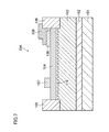
- FIG. 7 is a cross-sectional view of a semiconductor device including a field effect transistor actually fabricated based on the studies described above.
- a field effect transistor 204 shown in FIG. 7 a p-type AlGaN layer is used as the gate electrode 107 .
- the normally-off device was fabricated is that this field effect transistor is intended to be used as a power device and, in this case, the normally-off type is desirable from a practical standpoint.
- a normally-off device can be achieved as described above, and the device can be turned on by applying a predetermined gate voltage.
- any gate structure may be used for the field effect transistor.
- a metal electrode made of Ni, etc. coming into schottky contact with the nitride semiconductor layer 104 may be used as the gate electrode, or a MOS structure having an insulating film sandwiched between the gate electrode and the nitride semiconductor layer 104 may be formed. That is, any gate structure can be used without causing a trouble, and the collapse prevention/reduction technology described herein imposes no limitation on the structure of the gate electrode.
- the present inventors evaluated the on resistance at the time of switching of the fabricated field effect transistor 204 shown in FIG. 7 .
- FIGS. 8A and 8B are a circuit diagram and a waveform diagram, respectively, showing an evaluation system for the on resistance during switching of a field effect transistor.
- the on-resistance evaluation system shown in FIGS. 8A and 8B is a system for evaluating current collapse.
- the field effect transistor and the semiconductor device including the same are intended to be mounted in an air conditioner, etc. Therefore, to evaluate the on resistance in situations such as that where a motor used in the air conditioner, etc. is inverter-operated, the on resistance at the time of switching of the LR series load was evaluated.
- a reflux diode 804 is connected in parallel with the series circuit of the resistance load and the coil.
- the on resistance R ON of the field effect transistor at this switching is hereinafter referred to as “active R ON ” to distinguish this from the on voltage of the field effect transistor (under a low V dd condition) obtained by measurement of static characteristics (hereinafter referred to as “DC-R ON ”).
- the active R ON increases with increase of V dd when it is influenced by current collapse.
- the active R ON was measured in the following manner, to examine the V dd dependence: a pulse voltage having a period t period of 143 ⁇ s and an on time t ON of 7.5 ⁇ s was periodically given to the gate electrode 107 , and, after this was kept for a fixed time until the on voltage was stabilized, a waveform obtained immediately after the transistor was turned on (7 ⁇ s after the switching to the on state) was captured into an oscilloscope.
- the reason why the measurement time was set to a time immediately (7 ⁇ s) after the turning on is as follows. In the actual measurement using this measurement system, linking appeared under an influence of a parasitic capacitance of the evaluation system in the time range shorter than the above time, failing to perform correct measurement. The linking disappeared 7 ⁇ s after the switching to the on state, succeeding in measurement of the correct on voltage.
- FIG. 9 is a view showing the results of the evaluation of the field effect transistor 204 shown in FIG. 7 using the evaluation system shown in FIGS. 8A and 8B .
- the black circles ( ⁇ ) indicate the measurement results of the field effect transistor 204 shown in FIG. 7
- the black squares ( ⁇ ) indicate the relationship between the active R ON and V dd of the field effect transistor ( FIG. 4 ) having no p-type nitride semiconductor layer for hole injection measured for comparison.
- the active R ON has been reduced to a low value in the case of having hole injection, compared with the case of having no hole injection, in a high-V dd range (about 210 V or more in the illustrated measurement conditions).
- V dd 320 V
- the active R ON has been reduced to roughly the half in the case of having hole injection, compared with the case of having no hole injection, significantly exhibiting prevention or reduction of current collapse by hole injection.
- the active R ON is large in the case of having hole injection, compared with the case of having no hole injection.
- the present inventors have contemplated the reason for this as follows.
- FIGS. 10A to 10C are views diagrammatically showing band alignment in a region right under the electrode (terminal) 109 for hole injection when the electrode 109 is formed, in comparison with the case of forming no such electrode:
- FIG. 10A shows band alignment in a field effect transistor where neither the electrode 109 nor the p-type nitride semiconductor layer 108 for hole injection is formed
- FIG. 10B shows band alignment in the field effect transistor where both the electrode 109 and the p-type nitride semiconductor layer 108 for hole injection are formed.
- the potential of the nitride semiconductor layer 104 made of AlGaN increases under the influence of the p-type nitride semiconductor layer 108 , resulting in decrease in the concentration of the two-dimensional electron gas. This is considered to be the cause of increase in resistance right under the electrode 109 for hole injection.
- the present inventors have made an examination on reducing the resistance right under the p-type nitride semiconductor layer 108 (and the electrode 109 ) for hole injection thereby preventing or reducing the increase in active R ON in the low-V dd region.
- Si as an n-type impurity has been diffused in a portion of the nitride semiconductor layer 104 right under the p-type nitride semiconductor layer 108 , to form an n-type nitride semiconductor layer.
- FIG. 10C is a view showing band alignment in an under-gate region observed when an n-type impurity is diffused in a region located right under the electrode (terminal) 109 and the p-type nitride semiconductor layer 108 for hole injection.
- the potential of the nitride semiconductor layer made of AlGaN will decrease under the influence of the built-in potential at the p-n junction, resulting in increase in the concentration of the two-dimensional electron gas, and thus decreasing the channel resistance in this region.
- the direction from the p-type nitride semiconductor layer for hole injection toward the n-type nitride semiconductor layer right under the p-type nitride semiconductor layer is the forward direction. Holes are therefore injected without causing a trouble.
- the hole carrier concentration of the p-type nitride semiconductor layer be larger than the electron carrier concentration of the n-type nitride semiconductor layer. Specifically, it is desirable that the hole carrier concentration be of the order of 5 ⁇ 10 18 cm ⁇ 3 and the carrier concentration of the n-type nitride semiconductor layer be of the order of 1 ⁇ 10 18 cm ⁇ 3 . With such concentrations, it is considered possible to reduce the DC-R ON while maintaining the effect of preventing or reducing current collapse by hole injection.
- the present inventors fabricated a semiconductor device including the field effect transistor 200 of the embodiment shown in FIG. 1 , and the current collapse in this field effect transistor was examined.
- the configuration of the field effect transistor 200 of this embodiment shown in FIG. 1 is as described above, where the p-type nitride semiconductor layer 108 for hole injection made of GaN is formed on the nitride semiconductor layer 104 at a position between the gate electrode 107 and the drain electrode 106 . Further, the n-type nitride semiconductor layer 111 is formed in a region of the nitride semiconductor layer 104 made of AlGaN located right under the p-type nitride semiconductor layer 108 . The p-type nitride semiconductor layer 108 is electrically connected to the drain electrode via the electrode 109 made of Au, etc.
- Si is implanted in a portion of the nitride semiconductor layer 104 by ion implantation before formation of the p-type nitride semiconductor layer 108 . Thereafter, the Si ions are activated by annealing to form the n-type nitride semiconductor layer 111 .
- the black triangles ( ⁇ ) in FIG. 9 indicate the results of measurement of the relationship between the active R ON and V dd in the field effect transistor 200 shown in FIG. 1 formed in the manner described above. From the results, it has been found that, in the field effect transistor shown in FIG. 1 , the active R ON has decreased in the entire range measured, compared with the case of having hole injection without provision of the n-type nitride semiconductor layer. Also, the active R ON in the field effect transistor shown in FIG. 1 has been kept low in the entire range excluding when V dd is 100V, compared with the case of having no hole injection. Thus, it has been confirmed that, by fabricating the field effect transistor having the configuration shown in FIG. 1 , current collapse can be effectively prevented or reduced while the on resistance at DC electricity is kept to a low value.
- n-type nitride semiconductor layer 111 is formed by implanting an n-type impurity in a portion of the nitride semiconductor layer 104 in the field effect transistor 200 of this embodiment shown in FIG. 1 , it is also considered possible to prevent or reduce current collapse while reducing the on resistance by forming an n-type nitride semiconductor layer made of GaN, etc. between the nitride semiconductor layer 104 and the p-type nitride semiconductor layer 108 by MOCVD, ion implantation, etc.
- FIG. 11 is a cross-sectional view showing an alteration of the semiconductor device of the embodiment shown in FIG. 1 .
- the semiconductor device of this alteration includes a field effect transistor 206 where the n-type nitride semiconductor layer 111 of the field effect transistor (HEMT) 200 shown in FIG. 1 is replaced with an n-type nitride semiconductor layer 113 different in formation method and shape.
- HEMT field effect transistor
- the field effect transistor 206 of this alteration has a buffer layer 102 made of low-temperature AlN formed on a substrate 101 made of p-type Si, etc., a nitride semiconductor layer 103 formed on the buffer layer 102 , a nitride semiconductor layer 104 larger in bandgap than the nitride semiconductor layer 103 formed on the nitride semiconductor layer 103 , a gate electrode 107 formed on the nitride semiconductor layer 104 , and a source electrode 105 and a drain electrode 106 formed to sandwich the gate electrode 107 .
- the nitride semiconductor layer 103 has a thickness of the order of 0.5 ⁇ m to 3 ⁇ m and made of undoped GaN, for example.
- the nitride semiconductor layer 104 has a thickness of the order of 20 nm to 100 nm and made of undoped AlGaN, for example. Note however that the nitride semiconductor layers 103 and 104 are only required to be made of such nitride semiconductors that cause generation of two-dimensional electron gas 110 at the interface therebetween.
- the field effect transistor 206 uses this two-dimensional electron gas 110 as the channel.
- the gate electrode 107 is provided by forming a p-type AlGaN layer and a p-type GaN layer on top of each other in this order and then forming an electrode made of a metal such as Au by evaporation, for example.
- the source electrode 105 and the drain electrode 106 are provided to be in contact with at least the nitride semiconductor layer 104 .
- the source electrode 105 and the drain electrode 106 are formed on the nitride semiconductor layer 103 and in direct contact with the two-dimensional electron gas 110 .
- the source electrode 105 and the drain electrode 106 each have a Ti layer and an Al layer, for example.
- the source electrode 105 , the drain electrode 106 , and the gate electrode 107 have a strip-like planar shape, and may be placed to be substantially in parallel with one another.
- the field effect transistor 206 of this alteration further has a p-type nitride semiconductor layer 108 for hole injection formed on the nitride semiconductor layer 104 at a position between the gate electrode 107 and the drain electrode 106 and electrically connected to the drain electrode 106 .
- the p-type nitride semiconductor layer 108 is made of a nitride semiconductor such as GaN smaller in bandgap than the nitride semiconductor layer 104 , for example.
- Also formed is an electrode 109 connecting the p-type nitride semiconductor layer 108 to the drain electrode 106 .
- the electrode 109 is made of a metal such as Au, for example.
- the field effect transistor 206 of this alteration is different from the field effect transistor 200 shown in FIG. 1 in that the n-type nitride semiconductor layer 113 is formed in the nitride semiconductor layer 104 made of AlGaN, for example, extending from underneath the p-type nitride semiconductor layer 108 to the position in contact with the source electrode 105 and to the position in contact with the drain electrode 106 .
- the n-type impurity concentration of the n-type nitride semiconductor layer 113 is of the order of 10 17 cm ⁇ 3 to 5 ⁇ 10 18 cm ⁇ 3 .
- the DC-R ON can also be prevented or reduced.
- the n-type nitride semiconductor layer 113 can be formed by epitaxial growth of an n-type AlGaN layer, not by ion implantation, during the formation of the nitride semiconductor layer 104 , the manufacturing process can be simplified compared with the case of performing ion implantation.
- the n-type nitride semiconductor layer 113 is not necessarily required to be in direct contact with the p-type nitride semiconductor layer 108 as shown in FIG. 11 , the n-type nitride semiconductor layer 113 and the p-type nitride semiconductor layer 108 may form a p-n junction.
- the substrate 101 may be made of a compound semiconductor such as GaN, in addition to a Group 14 element such as Si, or may be made of an insulator such as sapphire.
- a GaN substrate it is unnecessary to form the buffer layer 102 shown in FIG. 1 , etc.
- the distance from the gate electrode 107 to the drain electrode 106 is made larger than the distance from the gate electrode 107 to the source electrode 105 for improving the electric strength, but the distances between the electrodes can be changed appropriately depending on the requirements such as the required electric strength.
- an insulating film made of SiN may be formed on the nitride semiconductor layer 104 to further ensure prevention or reduction of current collapse.
- a plurality of field effect transistors may be provided, or another semiconductor element and the inventive field effect transistor may be combined.
- the field effect transistor of an example of the present disclosure is useful as a power transistor used for a power supply circuit, etc. of a consumer appliance such as an air conditioner.
Landscapes
- Junction Field-Effect Transistors (AREA)
Abstract
Description
Claims (10)
Applications Claiming Priority (3)
| Application Number | Priority Date | Filing Date | Title |
|---|---|---|---|
| JP2011172983 | 2011-08-08 | ||
| JP2011-172983 | 2011-08-08 | ||
| PCT/JP2012/005020 WO2013021628A1 (en) | 2011-08-08 | 2012-08-07 | Semiconductor device |
Related Parent Applications (1)
| Application Number | Title | Priority Date | Filing Date |
|---|---|---|---|
| PCT/JP2012/005020 Continuation WO2013021628A1 (en) | 2011-08-08 | 2012-08-07 | Semiconductor device |
Publications (2)
| Publication Number | Publication Date |
|---|---|
| US20140138704A1 US20140138704A1 (en) | 2014-05-22 |
| US9018634B2 true US9018634B2 (en) | 2015-04-28 |
Family
ID=47668163
Family Applications (1)
| Application Number | Title | Priority Date | Filing Date |
|---|---|---|---|
| US14/165,405 Active US9018634B2 (en) | 2011-08-08 | 2014-01-27 | Semiconductor device |
Country Status (3)
| Country | Link |
|---|---|
| US (1) | US9018634B2 (en) |
| JP (1) | JP5903642B2 (en) |
| WO (1) | WO2013021628A1 (en) |
Cited By (4)
| Publication number | Priority date | Publication date | Assignee | Title |
|---|---|---|---|---|
| US10804369B2 (en) * | 2017-04-28 | 2020-10-13 | Mitsubishi Electric Corporation | Semiconductor device |
| US10833159B1 (en) | 2020-04-30 | 2020-11-10 | Innoscience (Suzhou) Technology Co., Ltd. | Semiconductor device and method for manufacturing the same |
| US11257942B2 (en) * | 2019-04-01 | 2022-02-22 | Nuvoton Technology Corporation Japan | Resistive element and power amplifier circuit |
| US11502170B2 (en) | 2020-03-23 | 2022-11-15 | Innoscience (Zhuhai) Technology Co., Ltd. | Semiconductor device and manufacturing method thereof |
Families Citing this family (19)
| Publication number | Priority date | Publication date | Assignee | Title |
|---|---|---|---|---|
| JP2014072377A (en) * | 2012-09-28 | 2014-04-21 | Fujitsu Ltd | Compound semiconductor device and manufacturing method of the same |
| JP6307351B2 (en) * | 2013-05-29 | 2018-04-04 | 株式会社豊田中央研究所 | Method and apparatus for observing heterojunction field effect transistor phenomena |
| JP6230456B2 (en) * | 2014-03-19 | 2017-11-15 | 株式会社東芝 | Semiconductor device |
| JP6293623B2 (en) | 2014-09-05 | 2018-03-14 | 株式会社東芝 | Semiconductor inspection equipment |
| IL303972A (en) | 2015-04-08 | 2023-08-01 | Novartis Ag | Cd20 therapies, cd22 therapies, and combination therapies with a cd19 chimeric antigen receptor (car) - expressing cell |
| US10332976B2 (en) * | 2015-08-28 | 2019-06-25 | Sharp Kabushiki Kaisha | Nitride semiconductor device |
| JP6657913B2 (en) * | 2015-12-16 | 2020-03-04 | 株式会社豊田中央研究所 | Semiconductor device and method of manufacturing semiconductor device |
| CN107230614B (en) * | 2016-03-25 | 2020-09-04 | 北京大学 | Preparation method of gallium nitride semiconductor device |
| CN105720097A (en) * | 2016-04-28 | 2016-06-29 | 中国科学院半导体研究所 | Enhanced-mode high electron mobility transistor, preparation method thereof, and semiconductor device |
| US10741682B2 (en) | 2016-11-17 | 2020-08-11 | Semiconductor Components Industries, Llc | High-electron-mobility transistor (HEMT) semiconductor devices with reduced dynamic resistance |
| US10854718B2 (en) | 2017-02-21 | 2020-12-01 | Semiconductor Components Industries, Llc | Method of forming a semiconductor device |
| JP7108386B2 (en) * | 2017-08-24 | 2022-07-28 | 住友化学株式会社 | Charge trap evaluation method |
| CN110391298B (en) * | 2018-04-23 | 2023-08-22 | 纳维达斯半导体有限公司 | Gallium Nitride Transistor Structure |
| CN110444597B (en) * | 2018-05-03 | 2021-03-19 | 苏州捷芯威半导体有限公司 | Semiconductor device and method for manufacturing the same |
| US10680069B2 (en) | 2018-08-03 | 2020-06-09 | Infineon Technologies Austria Ag | System and method for a GaN-based start-up circuit |
| JP7021034B2 (en) * | 2018-09-18 | 2022-02-16 | 株式会社東芝 | Semiconductor device |
| IL292924A (en) | 2019-11-26 | 2022-07-01 | Novartis Ag | Cd19 and cd22 chimeric antigen receptors and uses thereof |
| CN112786700A (en) * | 2020-04-30 | 2021-05-11 | 英诺赛科(苏州)半导体有限公司 | Semiconductor device with a plurality of transistors |
| JP2024135349A (en) * | 2023-03-22 | 2024-10-04 | 株式会社東芝 | Semiconductor device and its manufacturing method |
Citations (6)
| Publication number | Priority date | Publication date | Assignee | Title |
|---|---|---|---|---|
| US20040227211A1 (en) | 2003-05-16 | 2004-11-18 | Wataru Saito | Power semiconductor device used for power control |
| JP2006267476A (en) | 2005-03-23 | 2006-10-05 | Aisin Seiki Co Ltd | Sound absorber and sound absorber |
| WO2008062800A1 (en) | 2006-11-20 | 2008-05-29 | Panasonic Corporation | Semiconductor device and its drive method |
| JP2008172055A (en) | 2007-01-12 | 2008-07-24 | Sharp Corp | Nitride semiconductor device and power conversion device using the same |
| WO2010082272A1 (en) | 2009-01-16 | 2010-07-22 | 日本電気株式会社 | Semiconductor device and method for producing the same |
| JP2011151176A (en) | 2010-01-21 | 2011-08-04 | Toyota Central R&D Labs Inc | High electron mobility transistor |
-
2012
- 2012-08-07 WO PCT/JP2012/005020 patent/WO2013021628A1/en not_active Ceased
- 2012-08-07 JP JP2013527894A patent/JP5903642B2/en active Active
-
2014
- 2014-01-27 US US14/165,405 patent/US9018634B2/en active Active
Patent Citations (10)
| Publication number | Priority date | Publication date | Assignee | Title |
|---|---|---|---|---|
| US20040227211A1 (en) | 2003-05-16 | 2004-11-18 | Wataru Saito | Power semiconductor device used for power control |
| JP2004342907A (en) | 2003-05-16 | 2004-12-02 | Toshiba Corp | Power semiconductor device |
| JP2006267476A (en) | 2005-03-23 | 2006-10-05 | Aisin Seiki Co Ltd | Sound absorber and sound absorber |
| US20060260870A1 (en) | 2005-03-23 | 2006-11-23 | Nagata Kosakusho Co., Ltd. | Sound absorber and sound absorbing device |
| WO2008062800A1 (en) | 2006-11-20 | 2008-05-29 | Panasonic Corporation | Semiconductor device and its drive method |
| US20100097105A1 (en) | 2006-11-20 | 2010-04-22 | Tatsuo Morita | Semiconductor device and method for driving the same |
| JP2008172055A (en) | 2007-01-12 | 2008-07-24 | Sharp Corp | Nitride semiconductor device and power conversion device using the same |
| WO2010082272A1 (en) | 2009-01-16 | 2010-07-22 | 日本電気株式会社 | Semiconductor device and method for producing the same |
| US20110260217A1 (en) | 2009-01-16 | 2011-10-27 | Yasuhiro Okamoto | Semiconductor apparatus and method of manufacturing the same |
| JP2011151176A (en) | 2010-01-21 | 2011-08-04 | Toyota Central R&D Labs Inc | High electron mobility transistor |
Non-Patent Citations (4)
| Title |
|---|
| Binari, S.C., et al: "Fabrication and Characterization of GaN FETs", Solid State Electronics, vol. 41, No. 10, 1997, pp. 1549-1554. |
| International Search Report issued in PCT/JP2012/005020, dated Oct. 16, 2012, with English translation, 5 pages. |
| Uemoto, Y, et al.: "Gate Injection Transistor (GIT)-A Normally-Off AlGaN/GaN Power Transistor Using Conductivity Modulation", IEEE Transactions of Electron Devices, vol. 54, No. 12, Dec. 2007, pp. 3393-3399. |
| Vetury, R., et al.: "The Impact of Surface States on the DC and RF Characteristics of AlGaN/GaN HFETs", IEEE Transactions of Electron Devices, vol. 48, No. 3, Mar. 2001, pp. 560-566. |
Cited By (5)
| Publication number | Priority date | Publication date | Assignee | Title |
|---|---|---|---|---|
| US10804369B2 (en) * | 2017-04-28 | 2020-10-13 | Mitsubishi Electric Corporation | Semiconductor device |
| US11257942B2 (en) * | 2019-04-01 | 2022-02-22 | Nuvoton Technology Corporation Japan | Resistive element and power amplifier circuit |
| US11502170B2 (en) | 2020-03-23 | 2022-11-15 | Innoscience (Zhuhai) Technology Co., Ltd. | Semiconductor device and manufacturing method thereof |
| US10833159B1 (en) | 2020-04-30 | 2020-11-10 | Innoscience (Suzhou) Technology Co., Ltd. | Semiconductor device and method for manufacturing the same |
| US12094931B2 (en) | 2020-04-30 | 2024-09-17 | Innoscience (suzhou) Semiconductor Co., Ltd. | Semiconductor device and method for manufacturing the same |
Also Published As
| Publication number | Publication date |
|---|---|
| JP5903642B2 (en) | 2016-04-13 |
| JPWO2013021628A1 (en) | 2015-03-05 |
| WO2013021628A1 (en) | 2013-02-14 |
| US20140138704A1 (en) | 2014-05-22 |
Similar Documents
| Publication | Publication Date | Title |
|---|---|---|
| US9018634B2 (en) | Semiconductor device | |
| US10312339B2 (en) | Semiconductor device | |
| US9570438B1 (en) | Avalanche-rugged quasi-vertical HEMT | |
| US7816707B2 (en) | Field-effect transistor with nitride semiconductor and method for fabricating the same | |
| US9589951B2 (en) | High-electron-mobility transistor with protective diode | |
| US9196614B2 (en) | Inverted III-nitride P-channel field effect transistor with hole carriers in the channel | |
| US8390029B2 (en) | Semiconductor device for reducing and/or preventing current collapse | |
| JP4755961B2 (en) | Nitride semiconductor device and manufacturing method thereof | |
| US8729562B2 (en) | Semiconductor device and method for manufacturing same | |
| US9087889B2 (en) | Semiconductor devices with 2DEG and 2DHG | |
| US9190506B2 (en) | Field-effect transistor | |
| US8624667B2 (en) | High electron mobility transistors with multiple channels | |
| US20090121775A1 (en) | Transistor and method for operating the same | |
| US20100207164A1 (en) | Field effect transistor | |
| US20220359669A1 (en) | Nitride semiconductor device and method of manufacturing the same | |
| US20220254902A1 (en) | Nitride semiconductor device and method of fabricating the same | |
| US20120274402A1 (en) | High electron mobility transistor | |
| WO2014050740A1 (en) | Switching element | |
| US20130240894A1 (en) | Overvoltage Protection Device for Compound Semiconductor Field Effect Transistors | |
| KR20140059410A (en) | Power semiconductor device | |
| JP2011142358A (en) | Nitride semiconductor device | |
| JP2013239735A (en) | Field effect transistor | |
| JP2013172108A (en) | Semiconductor device and manufacturing method thereof | |
| JP5545653B2 (en) | Nitride semiconductor device | |
| EP4439677A1 (en) | Hemt device having an improved gate structure and manufacturing process thereof |
Legal Events
| Date | Code | Title | Description |
|---|---|---|---|
| AS | Assignment |
Owner name: PANASONIC CORPORATION, JAPAN Free format text: ASSIGNMENT OF ASSIGNORS INTEREST;ASSIGNORS:TANAKA, KENICHIRO;UEDA, TETSUZO;SIGNING DATES FROM 20131224 TO 20131227;REEL/FRAME:032873/0505 |
|
| AS | Assignment |
Owner name: PANASONIC INTELLECTUAL PROPERTY MANAGEMENT CO., LTD., JAPAN Free format text: ASSIGNMENT OF ASSIGNORS INTEREST;ASSIGNOR:PANASONIC CORPORATION;REEL/FRAME:034194/0143 Effective date: 20141110 Owner name: PANASONIC INTELLECTUAL PROPERTY MANAGEMENT CO., LT Free format text: ASSIGNMENT OF ASSIGNORS INTEREST;ASSIGNOR:PANASONIC CORPORATION;REEL/FRAME:034194/0143 Effective date: 20141110 |
|
| STCF | Information on status: patent grant |
Free format text: PATENTED CASE |
|
| FEPP | Fee payment procedure |
Free format text: PAYOR NUMBER ASSIGNED (ORIGINAL EVENT CODE: ASPN); ENTITY STATUS OF PATENT OWNER: LARGE ENTITY |
|
| MAFP | Maintenance fee payment |
Free format text: PAYMENT OF MAINTENANCE FEE, 4TH YEAR, LARGE ENTITY (ORIGINAL EVENT CODE: M1551); ENTITY STATUS OF PATENT OWNER: LARGE ENTITY Year of fee payment: 4 |
|
| AS | Assignment |
Owner name: PANASONIC INTELLECTUAL PROPERTY MANAGEMENT CO., LTD., JAPAN Free format text: CORRECTIVE ASSIGNMENT TO CORRECT THE ERRONEOUSLY FILED APPLICATION NUMBERS 13/384239, 13/498734, 14/116681 AND 14/301144 PREVIOUSLY RECORDED ON REEL 034194 FRAME 0143. ASSIGNOR(S) HEREBY CONFIRMS THE ASSIGNMENT;ASSIGNOR:PANASONIC CORPORATION;REEL/FRAME:056788/0362 Effective date: 20141110 |
|
| MAFP | Maintenance fee payment |
Free format text: PAYMENT OF MAINTENANCE FEE, 8TH YEAR, LARGE ENTITY (ORIGINAL EVENT CODE: M1552); ENTITY STATUS OF PATENT OWNER: LARGE ENTITY Year of fee payment: 8 |
|
| AS | Assignment |
Owner name: PANASONIC HOLDINGS CORPORATION, JAPAN Free format text: ASSIGNMENT OF ASSIGNORS INTEREST;ASSIGNOR:PANASONIC INTELLECTUAL PROPERTY MANAGEMENT CO., LTD.;REEL/FRAME:069503/0625 Effective date: 20241120 |
|
| AS | Assignment |
Owner name: PANASONIC HOLDINGS CORPORATION, JAPAN Free format text: ASSIGNMENT OF ASSIGNORS INTEREST;ASSIGNOR:INFINEON TECHNOLOGIES AUSTRIA AG;REEL/FRAME:072853/0508 Effective date: 20250901 |