US9009950B2 - Method for manufacturing high frequency inductor - Google Patents
Method for manufacturing high frequency inductor Download PDFInfo
- Publication number
- US9009950B2 US9009950B2 US13/804,250 US201313804250A US9009950B2 US 9009950 B2 US9009950 B2 US 9009950B2 US 201313804250 A US201313804250 A US 201313804250A US 9009950 B2 US9009950 B2 US 9009950B2
- Authority
- US
- United States
- Prior art keywords
- wafer
- forming
- copper
- high frequency
- frequency inductor
- Prior art date
- Legal status (The legal status is an assumption and is not a legal conclusion. Google has not performed a legal analysis and makes no representation as to the accuracy of the status listed.)
- Expired - Fee Related, expires
Links
Images


Classifications
-
- H—ELECTRICITY
- H01—ELECTRIC ELEMENTS
- H01F—MAGNETS; INDUCTANCES; TRANSFORMERS; SELECTION OF MATERIALS FOR THEIR MAGNETIC PROPERTIES
- H01F41/00—Apparatus or processes specially adapted for manufacturing or assembling magnets, inductances or transformers; Apparatus or processes specially adapted for manufacturing materials characterised by their magnetic properties
- H01F41/02—Apparatus or processes specially adapted for manufacturing or assembling magnets, inductances or transformers; Apparatus or processes specially adapted for manufacturing materials characterised by their magnetic properties for manufacturing cores, coils, or magnets
-
- H—ELECTRICITY
- H01—ELECTRIC ELEMENTS
- H01F—MAGNETS; INDUCTANCES; TRANSFORMERS; SELECTION OF MATERIALS FOR THEIR MAGNETIC PROPERTIES
- H01F17/00—Fixed inductances of the signal type
- H01F17/0006—Printed inductances
-
- H—ELECTRICITY
- H01—ELECTRIC ELEMENTS
- H01F—MAGNETS; INDUCTANCES; TRANSFORMERS; SELECTION OF MATERIALS FOR THEIR MAGNETIC PROPERTIES
- H01F41/00—Apparatus or processes specially adapted for manufacturing or assembling magnets, inductances or transformers; Apparatus or processes specially adapted for manufacturing materials characterised by their magnetic properties
- H01F41/02—Apparatus or processes specially adapted for manufacturing or assembling magnets, inductances or transformers; Apparatus or processes specially adapted for manufacturing materials characterised by their magnetic properties for manufacturing cores, coils, or magnets
- H01F41/04—Apparatus or processes specially adapted for manufacturing or assembling magnets, inductances or transformers; Apparatus or processes specially adapted for manufacturing materials characterised by their magnetic properties for manufacturing cores, coils, or magnets for manufacturing coils
- H01F41/041—Printed circuit coils
-
- H—ELECTRICITY
- H01—ELECTRIC ELEMENTS
- H01F—MAGNETS; INDUCTANCES; TRANSFORMERS; SELECTION OF MATERIALS FOR THEIR MAGNETIC PROPERTIES
- H01F17/00—Fixed inductances of the signal type
- H01F17/0006—Printed inductances
- H01F2017/0086—Printed inductances on semiconductor substrate
-
- Y—GENERAL TAGGING OF NEW TECHNOLOGICAL DEVELOPMENTS; GENERAL TAGGING OF CROSS-SECTIONAL TECHNOLOGIES SPANNING OVER SEVERAL SECTIONS OF THE IPC; TECHNICAL SUBJECTS COVERED BY FORMER USPC CROSS-REFERENCE ART COLLECTIONS [XRACs] AND DIGESTS
- Y10—TECHNICAL SUBJECTS COVERED BY FORMER USPC
- Y10T—TECHNICAL SUBJECTS COVERED BY FORMER US CLASSIFICATION
- Y10T29/00—Metal working
- Y10T29/49—Method of mechanical manufacture
- Y10T29/49002—Electrical device making
- Y10T29/4902—Electromagnet, transformer or inductor
- Y10T29/49021—Magnetic recording reproducing transducer [e.g., tape head, core, etc.]
- Y10T29/49032—Fabricating head structure or component thereof
- Y10T29/49048—Machining magnetic material [e.g., grinding, etching, polishing]
-
- Y—GENERAL TAGGING OF NEW TECHNOLOGICAL DEVELOPMENTS; GENERAL TAGGING OF CROSS-SECTIONAL TECHNOLOGIES SPANNING OVER SEVERAL SECTIONS OF THE IPC; TECHNICAL SUBJECTS COVERED BY FORMER USPC CROSS-REFERENCE ART COLLECTIONS [XRACs] AND DIGESTS
- Y10—TECHNICAL SUBJECTS COVERED BY FORMER USPC
- Y10T—TECHNICAL SUBJECTS COVERED BY FORMER US CLASSIFICATION
- Y10T29/00—Metal working
- Y10T29/49—Method of mechanical manufacture
- Y10T29/49002—Electrical device making
- Y10T29/4902—Electromagnet, transformer or inductor
- Y10T29/49021—Magnetic recording reproducing transducer [e.g., tape head, core, etc.]
- Y10T29/49032—Fabricating head structure or component thereof
- Y10T29/4906—Providing winding
- Y10T29/49064—Providing winding by coating
-
- Y—GENERAL TAGGING OF NEW TECHNOLOGICAL DEVELOPMENTS; GENERAL TAGGING OF CROSS-SECTIONAL TECHNOLOGIES SPANNING OVER SEVERAL SECTIONS OF THE IPC; TECHNICAL SUBJECTS COVERED BY FORMER USPC CROSS-REFERENCE ART COLLECTIONS [XRACs] AND DIGESTS
- Y10—TECHNICAL SUBJECTS COVERED BY FORMER USPC
- Y10T—TECHNICAL SUBJECTS COVERED BY FORMER US CLASSIFICATION
- Y10T29/00—Metal working
- Y10T29/49—Method of mechanical manufacture
- Y10T29/49002—Electrical device making
- Y10T29/49117—Conductor or circuit manufacturing
- Y10T29/49124—On flat or curved insulated base, e.g., printed circuit, etc.
-
- Y—GENERAL TAGGING OF NEW TECHNOLOGICAL DEVELOPMENTS; GENERAL TAGGING OF CROSS-SECTIONAL TECHNOLOGIES SPANNING OVER SEVERAL SECTIONS OF THE IPC; TECHNICAL SUBJECTS COVERED BY FORMER USPC CROSS-REFERENCE ART COLLECTIONS [XRACs] AND DIGESTS
- Y10—TECHNICAL SUBJECTS COVERED BY FORMER USPC
- Y10T—TECHNICAL SUBJECTS COVERED BY FORMER US CLASSIFICATION
- Y10T29/00—Metal working
- Y10T29/49—Method of mechanical manufacture
- Y10T29/49002—Electrical device making
- Y10T29/49117—Conductor or circuit manufacturing
- Y10T29/49204—Contact or terminal manufacturing
Definitions
- the present invention relates to a method for manufacturing a high frequency inductor, and more particularly, to a method for manufacturing a high frequency inductor capable of preventing a damage of an electrode and deterioration of a product performance by forming a barrier layer on an electrode and then filling an epoxy therein to perform a polishing process.
- a multi-layered inductor according to the related art is constructed by forming a laminate through a printing process and a laminating process for an inter-layer via connection between a coil pattern and a coil on a ceramic insulating layer and then compressing and firing the laminate.
- deformation of the coil is easily caused by an electrode blurring in a printing process and by an alignment distortion or an electrode press, or the like, at the time of laminating and compressing, and the deformation of the coil shape is increased due to contraction deformation at the time of firing. Therefore, it is difficult to control a desired inductance value of the inductor and to implement a low direct current resistance. As a result, it is difficult to secure high-Q characteristics required in the high frequency inductor.
- Patent Document 1 Korean Patent Laid-Open Publication No. 10-2002-0005749
- Patent Document 2 Japanese Patent Laid-Open Publication No. 2009-295759
- An object of the present invention is to provide a method for manufacturing a high frequency inductor capable of preventing a damage of electrode by forming a barrier layer on the electrode and then filling an epoxy therein to perform a polishing process, and capable of preventing a coupler (a dye) from affecting characteristics of elements by not using the coupler (the dye).
- a method for manufacturing a high frequency inductor including; forming a primary coil for manufacturing the high frequency inductor on a wafer; coating a primary PSV on the wafer on which the primary coil is formed; forming a secondary coil for manufacturing the high frequency inductor, after the coating of the primary PSV; coating a secondary PSV, after the forming of the secondary coil; forming a barrier layer on an electrode portion to be exposed of the high frequency inductor, after the coating of the secondary PSV; filling and curing an insulating resin on the wafer, after the forming of the barrier layer; and polishing the cured resin up to the barrier layer to expose the electrode.
- the forming of the primary coil may include coating a photoresist on the wafer; exposing the wafer on which the photoresist is coated; developing the wafer, after the exposing of the wafer; plating copper (Cu) on the wafer, after the developing of the wafer; stripping the photoresist, after the plating of the copper; and etching a copper seed layer that is previously formed on the wafer.
- the exposure may be performed by irradiating a light having light amount of 850 mJ on the wafer.
- the copper may be plated with a thickness of 12 ⁇ m.
- the forming of the secondary coil may include forming a copper seed layer on the wafer on which the coating of the primary PSV is completed; cleaning the wafer, after the forming of the copper seed layer; coating a photoresist on the wafer, after the cleaning of the wafer; exposing the wafer on which the photoresist is coated; developing the wafer, after the exposing of the wafer; plating copper (Cu) on the wafer, after the developing of the wafer; stripping the photoresist, after the plating of the copper; and etching the copper seed layer.
- the exposure may be performed by irradiating a light having light amount of 850 mJ on the wafer.
- the copper may be plated with a thickness of 5 ⁇ m.
- the barrier layer in the forming of the barrier layer may be formed of a thermosetting polymer or an ultraviolet curable polymer.
- the insulating resin in the filling of the insulating resin may be an epoxy resin.
- FIG. 1 is a diagram showing a state in which an epoxy is added with a coupler to be filled, after the last electrode is formed according to a method for manufacturing a high frequency inductor according to the related art.
- FIG. 2 is a flow chart showing an execution process of the method for manufacturing the high frequency inductor according to an exemplary embodiment of the present invention.
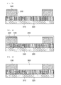
- FIGS. 3A to 3F are diagrams schematically describing main processes of the method for manufacturing the high frequency inductor according to the exemplary embodiment of the present invention.
- An inductor that is an electronic component needs anisotropic magnetic material combination and assembly and an airgap at the time of assembling the anisotropic magnetic material significantly affects an electrical characteristics.
- the airgap is electrically neutral, but the inductor that is a core type component using inductive magnetic field affects the electrical characteristics according to an existence or non-existence and creation degree of the airgap.
- the epoxy is used as a filler 150 . In this case, it is difficult to confirm exposure and polishing degrees of the electrode in a process of exposing the electrode due to transparent characteristics of the epoxy.
- a coupler (a dye) is added to the epoxy to secure a reliability of the process.
- the coupler due to the use of the coupler (dye), air bubbles may be generated in the epoxy, or physical properties of the filler 150 may be changed as compared to a pure epoxy, such that the characteristics of products (inductor) may be deteriorated.
- in polishing the epoxy to which the coupler is added it is still difficult to accurately confirm the polishing degree until the electrode is exposed, such that the electrode may be damaged.
- reference numeral 110 represents a wafer
- reference numeral 120 represents a coil, respectively.
- the present invention is proposed to solve the problems in the method for manufacturing the high frequency inductor according to the related art as described above.
- the present invention proposes a method for manufacturing a high frequency inductor capable of preventing a damage of electrode by forming a barrier layer on the electrode and then filling an epoxy therein to perform a polishing process, and capable of preventing a coupler (dye) from affecting characteristics of elements by not using the coupler (dye).
- FIG. 2 is a flow chart showing an execution process of the method for manufacturing the high frequency inductor according to an exemplary embodiment of the present invention.
- a primary coil for manufacturing the high frequency inductor is first formed on the wafer (S 201 ).
- a primary PSV is coated on the wafer on which the primary coil is formed (S 202 ).
- a secondary coil for manufacturing the high frequency inductor is formed (S 203 ).
- a secondary PSV is coated similar to the formation of the primary coil (S 204 ).
- a barrier layer is formed on a portion of the electrode to be exposed of the high frequency inductor (S 205 ).
- a thermosetting polymer or an ultraviolet curable polymer may be used as a material of the barrier layer.
- an insulating resin is filled on the wafer and is then cured (S 206 ).
- an epoxy resin may be used as the insulating resin.
- the cured resin is polished up to the barrier layer to thereby expose the electrode (S 207 ).
- a worker may perform the polishing process, while confirming the barrier layer from the beginning through the insulating resin, that is, the transparent epoxy resin, thereby easily confirming whether or not the electrode is exposed by the existence or non-existence of the barrier layer. As a result, the damage of the electrode due to the polishing may be prevented.
- the forming of the primary coil (S 201 ) may be configured to include coating a photoresist on the wafer; exposing the wafer on which the photoresist is coated; developing the wafer after the exposing; plating copper (Cu) on the wafer, after the developing; stripping the photoresist, after the plating of the copper (Cu); and etching a copper seed layer which is previously formed on the wafer.
- the exposure may be performed by irradiating a light having light amount of 850 mJ on the wafer.
- the light amount of 850 mJ as mentioned above corresponds to one design value for manufacturing a high frequency inductor having any specific specification, and is not necessarily limited to the light amount value.
- the copper (Cu) is plated with a thickness of 12 ⁇ m.
- the thickness of 12 ⁇ m for plating the copper (Cu) described above also corresponds to one design value for manufacturing a high frequency inductor having any specific specification, and is not necessarily limited to the thickness value.
- the forming of the secondary coil (S 203 ) may be configured to include forming a copper seed layer on the wafer on which the coating of the primary PSV is completed; cleaning the wafer, after the forming of the seed layer; coating a photoresist on the wafer, after the cleaning; exposing the wafer on which the photoresist is coated; developing the wafer, after the exposing; plating a copper (Cu) on the wafer, after the developing; stripping the photoresist, after the plating of the copper; and etching the copper seed layer.
- the exposure may be performed by irradiating a light having light amount of 850 mJ on the wafer.
- the light amount of 850 mJ as described above corresponds to one design value for manufacturing a high frequency inductor having any specific specification, and is not necessarily limited to the light amount value.
- the copper (Cu) is plated with a thickness of 5 ⁇ m.
- the thickness of 5 ⁇ m for plating the copper as described above similarly corresponds to one design value for manufacturing a high frequency inductor having any specific specification, and is not necessarily limited to the thickness value.
- FIGS. 3A to 3F are diagrams schematically describing main processes of the method for manufacturing the high frequency inductor according to the exemplary embodiment of the present invention as described above.
- the barrier layer 340 is formed on the portion of the electrode 330 to be exposed of the high frequency inductor using an off-set printing (S 205 ).
- the insulating resin (epoxy resin) 350 is filled and cured on the wafer 310 (S 206 ).
- the cured resin (epoxy resin) 350 is polished up to the barrier layer 340 to expose the electrode 330 (S 207 ).
- the barrier layer is formed on the electrode and then is filled with the insulating resin therein, such that it is easy to confirm whether or not the electrode is exposed by the existence or non-existence of the barrier layer when performing an exposure process of the electrode, thereby making it possible to prevent the damage of the electrode due to the polishing.
- the dispersion process of the dye for coloring into the polymer such as the epoxy used as the filler, is removed, thereby making it possible to prevent the dye according to the related art from adversely affecting the characteristics of the elements.
Landscapes
- Engineering & Computer Science (AREA)
- Power Engineering (AREA)
- Manufacturing & Machinery (AREA)
- Microelectronics & Electronic Packaging (AREA)
- Manufacturing Cores, Coils, And Magnets (AREA)
- Coils Or Transformers For Communication (AREA)
- Semiconductor Integrated Circuits (AREA)
- Internal Circuitry In Semiconductor Integrated Circuit Devices (AREA)
Abstract
Description
Claims (9)
Applications Claiming Priority (2)
| Application Number | Priority Date | Filing Date | Title |
|---|---|---|---|
| KR10-2012-0063825 | 2012-06-14 | ||
| KR1020120063825A KR101709810B1 (en) | 2012-06-14 | 2012-06-14 | Method for manufacturing high frequency inductor |
Publications (2)
| Publication Number | Publication Date |
|---|---|
| US20130333202A1 US20130333202A1 (en) | 2013-12-19 |
| US9009950B2 true US9009950B2 (en) | 2015-04-21 |
Family
ID=49754590
Family Applications (1)
| Application Number | Title | Priority Date | Filing Date |
|---|---|---|---|
| US13/804,250 Expired - Fee Related US9009950B2 (en) | 2012-06-14 | 2013-03-14 | Method for manufacturing high frequency inductor |
Country Status (3)
| Country | Link |
|---|---|
| US (1) | US9009950B2 (en) |
| JP (1) | JP6324666B2 (en) |
| KR (1) | KR101709810B1 (en) |
Families Citing this family (2)
| Publication number | Priority date | Publication date | Assignee | Title |
|---|---|---|---|---|
| KR102426202B1 (en) | 2017-01-09 | 2022-07-29 | 삼성전기주식회사 | Printed circuit board |
| KR101994754B1 (en) | 2017-08-23 | 2019-07-01 | 삼성전기주식회사 | Inductor |
Citations (4)
| Publication number | Priority date | Publication date | Assignee | Title |
|---|---|---|---|---|
| KR20020005749A (en) | 2000-03-17 | 2002-01-17 | 모리시타 요이찌 | Module with built-in electronic elements and method of manufacture thereof |
| US6641984B2 (en) * | 2000-05-16 | 2003-11-04 | Tdk Corporation | Method of frame plating and method of forming magnetic pole of thin-film magnetic head |
| US7018548B2 (en) * | 2002-07-19 | 2006-03-28 | Tdk Corporation | Conductive thin film pattern and method of forming the same, method of manufacturing thin film magnetic head, method of manufacturing thin film inductor, and method of manufacturing micro device |
| JP2009295759A (en) | 2008-06-04 | 2009-12-17 | Shindengen Electric Mfg Co Ltd | Surface mount inductor, and manufacturing method of surface mount inductor |
Family Cites Families (12)
| Publication number | Priority date | Publication date | Assignee | Title |
|---|---|---|---|---|
| JP2914860B2 (en) * | 1992-10-20 | 1999-07-05 | 株式会社東芝 | Semiconductor device, method of manufacturing the same, polishing method, polishing apparatus and method for regenerating polished surface of polishing apparatus |
| US5370766A (en) * | 1993-08-16 | 1994-12-06 | California Micro Devices | Methods for fabrication of thin film inductors, inductor networks and integration with other passive and active devices |
| JP3623834B2 (en) * | 1995-01-31 | 2005-02-23 | 富士通株式会社 | Semiconductor memory device and manufacturing method thereof |
| JP2001244372A (en) * | 2000-03-01 | 2001-09-07 | Seiko Epson Corp | Semiconductor device and method of manufacturing the same |
| JP4055978B2 (en) * | 2000-10-02 | 2008-03-05 | Tdk株式会社 | Manufacturing method of high frequency coil |
| KR100426088B1 (en) | 2002-01-31 | 2004-04-06 | 삼성전자주식회사 | Self organizing learning petri nets |
| JP2007073611A (en) * | 2005-09-05 | 2007-03-22 | Renesas Technology Corp | Electronic device and manufacturing method thereof |
| JP2009253233A (en) * | 2008-04-10 | 2009-10-29 | Taiyo Yuden Co Ltd | Inner-layer substrate for common-mode choke coil, its manufacturing method, and common-mode choke coil |
| KR101174327B1 (en) * | 2008-09-30 | 2012-08-16 | 티디케이가부시기가이샤 | Composite electronic device, manufacturing method thereof, and connection structure of composite electronic device |
| JP2011071457A (en) * | 2008-12-22 | 2011-04-07 | Tdk Corp | Electronic component and manufacturing method of electronic component |
| JP5093210B2 (en) * | 2009-10-20 | 2012-12-12 | Tdk株式会社 | Coil component and manufacturing method thereof |
| JP5195876B2 (en) * | 2010-11-10 | 2013-05-15 | Tdk株式会社 | Coil component and manufacturing method thereof |
-
2012
- 2012-06-14 KR KR1020120063825A patent/KR101709810B1/en not_active Expired - Fee Related
-
2013
- 2013-03-14 US US13/804,250 patent/US9009950B2/en not_active Expired - Fee Related
- 2013-05-29 JP JP2013112727A patent/JP6324666B2/en active Active
Patent Citations (4)
| Publication number | Priority date | Publication date | Assignee | Title |
|---|---|---|---|---|
| KR20020005749A (en) | 2000-03-17 | 2002-01-17 | 모리시타 요이찌 | Module with built-in electronic elements and method of manufacture thereof |
| US6641984B2 (en) * | 2000-05-16 | 2003-11-04 | Tdk Corporation | Method of frame plating and method of forming magnetic pole of thin-film magnetic head |
| US7018548B2 (en) * | 2002-07-19 | 2006-03-28 | Tdk Corporation | Conductive thin film pattern and method of forming the same, method of manufacturing thin film magnetic head, method of manufacturing thin film inductor, and method of manufacturing micro device |
| JP2009295759A (en) | 2008-06-04 | 2009-12-17 | Shindengen Electric Mfg Co Ltd | Surface mount inductor, and manufacturing method of surface mount inductor |
Also Published As
| Publication number | Publication date |
|---|---|
| JP2014003289A (en) | 2014-01-09 |
| US20130333202A1 (en) | 2013-12-19 |
| JP6324666B2 (en) | 2018-05-16 |
| KR20130140431A (en) | 2013-12-24 |
| KR101709810B1 (en) | 2017-03-08 |
Similar Documents
| Publication | Publication Date | Title |
|---|---|---|
| US10304620B2 (en) | Thin film type inductor and method of manufacturing the same | |
| US9183979B2 (en) | Chip inductor and method for manufacturing the same | |
| US20130300527A1 (en) | Method of manufacturing coil element and coil element | |
| US9496213B2 (en) | Integrated device package comprising a magnetic core inductor with protective ring embedded in a package substrate | |
| US20160240514A1 (en) | Package structure and its fabrication method | |
| US20150028984A1 (en) | Thin film type inductor and method of manufacturing the same | |
| US9748652B2 (en) | Manufacturing method for a magnetic material core-embedded resin multilayer board | |
| US10672554B2 (en) | Inductor component and method for manufacturing the same | |
| JP4317107B2 (en) | Electronic device having organic material insulating layer and method for manufacturing the same | |
| US10115521B2 (en) | Manufacturing method for electronic component | |
| US20160381792A1 (en) | Printed circuit board and method of manufacturing the same | |
| CN114568034A (en) | Coil component and method for manufacturing same | |
| US20140285304A1 (en) | Inductor and method for manufacturing the same | |
| JPWO2012042668A1 (en) | Component built-in substrate and method for manufacturing component built-in substrate | |
| US20200143984A1 (en) | Magnetic element and method for manufacturing same | |
| JP2006098514A (en) | Method for forming photosensitive polyimide pattern and electronic element having the pattern | |
| JP2018078133A (en) | Built-in coil glass substrate and build-up substrate | |
| US9009950B2 (en) | Method for manufacturing high frequency inductor | |
| JP2023062846A (en) | Coil component and manufacturing method thereof | |
| US9440378B2 (en) | Planar electronic device and method for manufacturing | |
| JP2013128110A (en) | Manufacturing method for noise removal filter | |
| US20110193672A1 (en) | Magnetic element and method for manufacturing the same | |
| CN119153191A (en) | Printed circuit board integrated with magnetic inductor and manufacturing method thereof | |
| US11705276B2 (en) | Method for manufacturing electronic-component | |
| US20210134525A1 (en) | Thin-film inductor and method for manufacturing the same |
Legal Events
| Date | Code | Title | Description |
|---|---|---|---|
| AS | Assignment |
Owner name: SAMSUNG ELECTRO-MECHANICS CO., LTD, KOREA, REPUBLI Free format text: ASSIGNMENT OF ASSIGNORS INTEREST;ASSIGNORS:LEE, SANG MOON;YOO, YOUNG SEUCK;LEE, JONG YEN;AND OTHERS;REEL/FRAME:030008/0040 Effective date: 20121203 |
|
| FEPP | Fee payment procedure |
Free format text: PAYOR NUMBER ASSIGNED (ORIGINAL EVENT CODE: ASPN); ENTITY STATUS OF PATENT OWNER: LARGE ENTITY |
|
| STCF | Information on status: patent grant |
Free format text: PATENTED CASE |
|
| MAFP | Maintenance fee payment |
Free format text: PAYMENT OF MAINTENANCE FEE, 4TH YEAR, LARGE ENTITY (ORIGINAL EVENT CODE: M1551); ENTITY STATUS OF PATENT OWNER: LARGE ENTITY Year of fee payment: 4 |
|
| FEPP | Fee payment procedure |
Free format text: MAINTENANCE FEE REMINDER MAILED (ORIGINAL EVENT CODE: REM.); ENTITY STATUS OF PATENT OWNER: LARGE ENTITY |
|
| LAPS | Lapse for failure to pay maintenance fees |
Free format text: PATENT EXPIRED FOR FAILURE TO PAY MAINTENANCE FEES (ORIGINAL EVENT CODE: EXP.); ENTITY STATUS OF PATENT OWNER: LARGE ENTITY |
|
| STCH | Information on status: patent discontinuation |
Free format text: PATENT EXPIRED DUE TO NONPAYMENT OF MAINTENANCE FEES UNDER 37 CFR 1.362 |
|
| FP | Lapsed due to failure to pay maintenance fee |
Effective date: 20230421 |