US9009571B2 - Storage medium, system and method utilizing the same - Google Patents

Storage medium, system and method utilizing the same Download PDF

Info

Publication number
US9009571B2
US9009571B2 US13/947,979 US201313947979A US9009571B2 US 9009571 B2 US9009571 B2 US 9009571B2 US 201313947979 A US201313947979 A US 201313947979A US 9009571 B2 US9009571 B2 US 9009571B2
Authority
US
United States
Prior art keywords
controller
memory cell
module
data
corrected
Prior art date
Legal status (The legal status is an assumption and is not a legal conclusion. Google has not performed a legal analysis and makes no representation as to the accuracy of the status listed.)
Active, expires
Application number
US13/947,979
Other versions
US20140136929A1 (en
Inventor
Cheng-Wei Liu
Hsu-Ping Ou
Current Assignee (The listed assignees may be inaccurate. Google has not performed a legal analysis and makes no representation or warranty as to the accuracy of the list.)
Silicon Motion Inc
Original Assignee
Silicon Motion Inc
Priority date (The priority date is an assumption and is not a legal conclusion. Google has not performed a legal analysis and makes no representation as to the accuracy of the date listed.)
Filing date
Publication date
Application filed by Silicon Motion Inc filed Critical Silicon Motion Inc
Assigned to SILICON MOTION, INC. reassignment SILICON MOTION, INC. ASSIGNMENT OF ASSIGNORS INTEREST (SEE DOCUMENT FOR DETAILS). Assignors: LIU, Cheng-wei, OU, HSU-PING
Publication of US20140136929A1 publication Critical patent/US20140136929A1/en
Application granted granted Critical
Publication of US9009571B2 publication Critical patent/US9009571B2/en
Active legal-status Critical Current
Adjusted expiration legal-status Critical

Links

Images

Classifications

    • GPHYSICS
    • G06COMPUTING; CALCULATING OR COUNTING
    • G06FELECTRIC DIGITAL DATA PROCESSING
    • G06F11/00Error detection; Error correction; Monitoring
    • G06F11/07Responding to the occurrence of a fault, e.g. fault tolerance
    • G06F11/08Error detection or correction by redundancy in data representation, e.g. by using checking codes
    • G06F11/10Adding special bits or symbols to the coded information, e.g. parity check, casting out 9's or 11's
    • G06F11/1008Adding special bits or symbols to the coded information, e.g. parity check, casting out 9's or 11's in individual solid state devices
    • G06F11/1048Adding special bits or symbols to the coded information, e.g. parity check, casting out 9's or 11's in individual solid state devices using arrangements adapted for a specific error detection or correction feature

Definitions

  • the invention relates to an access system, and more particularly to an access system comprising a plurality of storing modules.
  • a NAND flash memory is a commonly used storage medium and widely used in electronic products. NAND flash memories can be manufactured into memory cards or USB disks.
  • the flash memory cards comprise Compact Flash (CF) cards, Multi Media Cards (MMCs), an embedded MultiMediaCards (eMMCs), a Smart Media (SM) cards, and a Secured Digital (SD) cards.
  • CF Compact Flash
  • MMCs Multi Media Cards
  • eMMCs embedded MultiMediaCards
  • SM Smart Media
  • SD Secured Digital
  • the flash memory card when a flash memory card is abnormal, the flash memory card cannot communicate with a host. For example, when the flash memory card executes an Error Checking and Correcting (ECC) operation, if the operation fails to correct the errors, the host device cannot receive correction data from the flash memory card during a read cycle.
  • ECC Error Checking and Correcting
  • a storage medium receives write data provided by a host device, provides read data to the host and comprises a first module and a second module.
  • the first module comprises a first memory cell and a first controller.
  • the first memory cell stores the write data.
  • the first controller reads the first memory cell to generate a first accessing result.
  • the second module comprises a second memory cell and a second controller.
  • the second memory cell stores the write data.
  • the second controller reads the second memory cell.
  • an access system comprises a host device and a storage medium.
  • the host device provides write data or receives read data.
  • the storage medium communicates with the host device and comprises a first module and a second module.
  • the first module comprises a first memory cell and a first controller.
  • the first memory cell stores the write data.
  • the first controller reads the first memory cell to generate a first accessing result.
  • the second module comprises a second memory cell and a second controller.
  • the second memory cell stores the write data.
  • the second controller reads the second memory cell.
  • the first controller requests the second controller to read the second memory cell to generate a second accessing result, and the second controller serves the second accessing result as the read data and provides the read data to the host device.
  • the storage medium comprises a first module and a second module.
  • the first module comprises a first controller and a first memory cell.
  • the second module comprises a second controller and a second memory cell.
  • An exemplary embodiment of the access method for the storage medium is described in the following.
  • the first controller is activated to receive a read command.
  • the first memory cell is read to generate a first accessing result according to the read command.
  • the second controller is requested by the first controller to read the second memory cell to generate a second accessing result and serves the second accessing result as read data when the first accessing result has an error and the error cannot be corrected.
  • the read data is provided to a host device.
  • FIG. 1 is a schematic diagram of an exemplary embodiment of an access system of the invention
  • FIG. 2 is a schematic diagram of an exemplary embodiment of a storage medium
  • FIGS. 3-6 are flow charts of other exemplary embodiments of an access method.
  • FIG. 1 is a schematic diagram of an exemplary embodiment of an access system of the invention.
  • the access system 100 comprises a host device 110 and a storage medium 120 .
  • the host device 110 writes data to the storage medium 120 or reads data from the storage medium 120 .
  • the invention does not limit the kind of the storage medium 120 .
  • Any device can serve as the storage medium 120 , as long as the device has a storing function.
  • the storage medium 120 is a Secure Digital (SD) card and communicates with the host device 110 according to an SD protocol. As shown in FIG. 1 , in the SD protocol, a plurality of transmittal lines Vdd, Clock, CMD, DAT0 ⁇ DAT3 are utilized.
  • the storage medium 120 is an embedded MultiMediaCard (eMMC).
  • eMMC embedded MultiMediaCard
  • the storage medium 120 comprises storing modules M 1 ⁇ M n .
  • the invention does not limit the kinds of the storing modules M 1 ⁇ M n .
  • the storing modules M 1 ⁇ M n are micro SD cards.
  • Each of the storing modules M 1 ⁇ M n comprises a card identification number and the card identification numbers are different.
  • One of the storing modules M 1 ⁇ M n is served as a main module and the others are served as sub-modules according to the card identification numbers.
  • the card identification numbers of the storing modules M 1 serving as a main module are set to 0
  • the card identification numbers of the storing modules M 2 ⁇ M n serving as sub-modules are set to other numbers, which exceed that of the storing module M 1 .
  • the host device 110 determines whether the storage medium 120 is ready. Since the storing module M 1 is served as a main module, the storing module M 1 provides a response signal to the host device 110 after all of the storing modules M 1 ⁇ M n are ready. In this embodiment, the storing module M 1 utilizes at least one transmittal line to determine whether the storing modules M 2 ⁇ M n are ready. Taking the SD protocol as an example, the storing module M 1 communicates with the storing modules M 2 ⁇ M n via the transmittal lines DAT1 and DAT2.
  • the storing module M 1 When one of the storing modules M 1 ⁇ M n is not ready, the storing module M 1 provides an unready response to the host device 110 . The host device 110 sends an ask command again until the storing module M 1 provides a read response. In one embodiment, when the storing modules M 1 ⁇ M n are ready, the storing module M 1 sets the level of the transmittal line DAT0 to a low level. The host device 110 determines that the storage medium 120 is ready according to the level of the transmittal line DAT0.
  • the host device 110 transmits write data to the storage medium 120 .
  • the storing module M 1 provides a response signal to the host device 110 .
  • the storing module M 1 sets the level of the transmittal line DAT0 to the low level.
  • the storing module M 1 reads data, which is stored in the storing module M 1 to generate a first accessing result according to address information and executes an Error Checking and Correcting (ECC) operation for the first accessing result.
  • ECC Error Checking and Correcting
  • the storing module M 1 corrects the first accessing result to generate corrected data, serves the corrected data as read data and provides the read data to the host device 110 via the transmittal lines DAT0 ⁇ DAT3.
  • the host device 110 determines that the storage medium 120 is ready to provide read data.
  • the storing module M 1 requests one of the storing modules M 2 ⁇ M n to serve as a new main module. In one embodiment, if the card identification number of the storing module M 2 is less than each of the card identification numbers of the storing modules M 3 ⁇ M n , the storing module M 2 is served as the new main module.
  • the storing module M 2 reads data, which is stored in the storing module M 2 to generate a second accessing result and executes an ECC operation for the second accessing result.
  • the storing module M 2 corrects the second accessing result to generate corrected data, serves the corrected data as read data and provides the read data to the host device 110 via the transmittal lines DAT0 ⁇ DAT3.
  • the storing module M 2 sets each level of the transmittal lines DAT0 ⁇ DAT3 to the low level to represent that the read data is ready.
  • the storing module M 1 when the storing module M 1 requests the storing module M 2 to provide the read data to the host device 110 , the storing module M 2 serves as a main module. At this time, the storing module M 1 can serve as a sub-module or not be utilized.
  • the new main module such as the storing module M 2
  • the storing module M 2 cannot provide the corrected data to the host device 110
  • another sub-module such as the storing module M 1 or one of the storing modules M 3 ⁇ M n , is requested by the storing module M 2 to serve as a main module to provide data to the host device 110 .
  • a memory cell when a memory cell is abnormal, the memory cell cannot provide data to a host device.
  • the storage medium 120 comprises various storing modules, when the main module is abnormal, another storing module provides data to the host device 110 . Thus, the transmittal state between the host device 110 and the storing module 120 can be maintained.
  • the storing module M 1 when the storing module M 1 cannot provide correction data to the host device 110 , the storing module M 2 provides data, which is stored in the storing module M 2 to the host device 110 and the storing module M 1 updates data, which is stored in the storing module M 1 according to the data provided by the storing module M 2 .
  • the storing module M 1 can serve as a sub-module.
  • the invention does not limit the kind of the protocol between the storing modules M 1 ⁇ M n .
  • the protocol between the storing modules M 1 ⁇ M n is an SD protocol.
  • the protocol between the storing modules M 1 ⁇ M n is a protocol, which transmits data via two wires.
  • the protocol may be an inter-integrated circuit (I2C) protocol or a universal asynchronous receiver transmitter (UART) protocol.
  • FIG. 2 is a schematic diagram of an exemplary embodiment of a storage medium.
  • the storing module M 1 comprises a controller 211 and a memory cell 212 .
  • the storing module M 2 comprises a controller 221 and a memory cell 222 .
  • the controller 211 accesses the memory cell 212 .
  • the controller 221 accesses the memory cell 222 .
  • the memory cells 212 and 222 are independent of NAND flash memories. Thus, the memory cells 212 and 222 are accessed by a single controller.
  • the storing module M 1 comprises an ECC engine 213 and the storing module M 2 comprises an ECC engine 223 .
  • the ECC engine 213 corrects the data received by the controller 211 .
  • the ECC engine 223 corrects the data received by the controller 221 .
  • the controller 211 reads data stored in the memory cell 212 to generate an accessing result and provides the accessing result to the ECC engine 213 to correct errors.
  • the ECC engine 213 corrects the accessing result to generate a corrected result and provides the corrected result to the controller 211 .
  • the ECC engine 213 is integrated in the controller 211 .
  • the controller 211 reads the memory cell 212 to generate a first accessing result according to address information.
  • the controller 211 utilizes the ECC engine 213 to execute an ECC operation for the first accessing result.
  • the controller 211 corrects the first accessing result to generate corrected data, serves the corrected data as read data and provides the read data to the host device 110 via the transmittal lines DAT0 ⁇ DAT3.
  • the storing module M 1 requests the storing module M 2 to serve as a main module.
  • the controller 221 reads the memory cell 222 to generate a second accessing result and utilizes the ECC engine 223 to execute an ECC operation for the second accessing result.
  • the controller 221 corrects the second accessing result to generate corrected data, serves the corrected data as read data and provides the read data to the host device 110 via the transmittal lines DAT0 ⁇ DAT3.
  • the controller 211 when the controller 211 cannot provide correction data to the host device 110 , the controller 221 is utilized to provide data to the host device 110 according to address information.
  • the controller 211 stores the data, which is provided by the controller 221 , to the memory cell 212 according to the address information.
  • the storing module M 1 may serve as a main module again or serve as a sub-module.
  • FIG. 3 is a flow chart of an exemplary embodiment of an access method.
  • the access method is applied to a storage medium.
  • the storage medium comprises a first module M 1 and a second module M 2 .
  • the first module M 1 comprises a first controller 211 and a first memory cell 212 .
  • the second module M 2 comprises a second controller 221 and a second memory cell 222 .
  • the first module M 1 is a main module and the second module M 2 is a sub-module.
  • a read command is received (step 311 ).
  • the read command is sent from a host device.
  • the first module M 1 is a main module
  • the first controller 211 reads data stored in the first memory cell 212 to generate a first accessing result according to address information of the read command.
  • the second module M 2 is read to generate a second accessing result and the second accessing result serves as read data (step 313 ).
  • the first controller 211 requests the second controller 221 to read the second memory cell 222 .
  • the second controller 221 reads the second memory cell 222 to generate a second accessing result according to the address information of the read command.
  • the invention does not limit the kind of the protocol between the first and the second controllers.
  • the first controller 211 communicates with the second controller 221 according to an SD protocol, an I2C protocol or an UART protocol.
  • the corrected accessing result serves as read data (step 314 ).
  • the read data is provided to a host device (step 315 ).
  • the second accessing result is stored in the first memory cell according to address information.
  • FIG. 4 is a flow chart of another exemplary embodiment of the access method.
  • write data is received (step 411 ).
  • the write data is provided by a host device.
  • the write data is stored in the first module M 1 and the second module M 2 .
  • the first module M 1 and the second module M 2 are idle (step 412 ). In this embodiment, since the first module M 1 is a main module, the first module M 1 determines whether the second module M 2 has completed a writing operation, which stores the write data in the memory cell 222 . In one embodiment, the first module M 1 determines whether the second module M 2 has completed the writing operation according to the levels of the transmittal lines DAT1 and DAT2 of an SD protocol.
  • the first module M 1 and the second module M 2 are idle, it represents that each of the first module M 1 and the second module M 2 has completed the writing operation.
  • a finish response is sent to the host device (step 415 ) and the writing operation is ended (step 416 ).
  • the first module M 1 sends the finish response to the host device.
  • the first module M 1 sets the level of the transmittal line DAT0 to a high level.
  • the first module M 1 or the second module M 2 When the first module M 1 or the second module M 2 is not idle, it represents that one of the first module M 1 and the second module M 2 has not completed the writing operation. Thus, an unfinished response is sent to the host device (step 413 ). In this embodiment, when one of the first module M 1 or the second module M 2 has not completed the writing operation, the first module M 1 sets the level of the transmittal line DAT0 to a low level and the first module M 1 or the second module M 2 continuously stores the write data (step 414 ).
  • FIG. 5 is a flowchart of another exemplary embodiment of an access method.
  • an asking command is received (step 511 ).
  • a host device sends the asking command.
  • the host device Before executing a writing operation and a read operation, the host device sends an asking command to a storage medium.
  • the first module M 1 serves as a main module such that the first module M 1 determines whether the module M 2 is ready via the transmittal lines DAT1 and DAT2.
  • the first module M 1 comprises an operating conditions register (OCR).
  • OCR has a busy bit, which is referred to as a card power-up status bit. When the busy bit is 1, it represents that the first module M 1 and the second module M 2 are ready. When the busy bit is 0, it represents that the first module M 1 or the second module M 2 is not ready. After all modules are ready, the first module M 1 sets the busy bit to 1.
  • the host device reads the busy bit of the OCR of the first module M 1 to determine whether the first module M 1 and the second module M 2 are ready.
  • a ready response is sent to the host device (step 513 ) and the initiate operation is ended (step 514 ).
  • the ready response sets the busy bit of the OCR to 1.
  • the first module M 1 communicates with the second module M 2 via the transmittal lines DAT1 and DAT2.
  • step 515 sets the busy bit of the OCR of the first module M 1 to 0, and step 516 provides all bit statuses of the OCR to the host device.
  • the host device determines that the first module M 1 or the second module M 2 is not ready according to the busy bit of the OCR and sends an asking command to the storage medium until the first module M 1 and the second module M 2 are ready.
  • FIG. 6 is a flowchart of an exemplary embodiment of an access method.
  • the storage medium is an SD card.
  • an SD command is received (step 611 ).
  • a host device sends a corresponding command to initial the storage medium according to the kind of the storage medium.
  • the first module M 1 determines whether the storage medium is idle (step 612 ).
  • the first module M 1 determines whether the second module M 2 is idle via the transmittal lines DAT1 and DAT2.
  • an idle response is sent to the host device (step 613 ).
  • the first module M 1 sets the level of the transmittal line DAT0 to an idle level, such as a high level.
  • the host device determines that the storage medium is idle according to the level of the transmittal line DAT0.
  • step 614 a non-idle response is sent to the host device (step 614 ) and step 612 is executed to determine whether the first module M 1 and the second module M 2 are ready.
  • the first module M 1 sets the level of the transmittal line DAT0 to a busy level, such as a low level.
  • the storage medium comprises a plurality of storing modules and each storing module stores the same data
  • a main storing module among the storing modules communicates with the host device and the other storing modules.
  • the main storing module stores data and provides a portion of the data to the host device.
  • the main storing module provides the data to the host device, if the data has many incorrect bits and the main storing module cannot correct the incorrect bits, another storing module is selected to communicate with the host device.
  • the host device can normally execute an accessing operation.

Abstract

A storage medium receiving write data provided by a host device, providing read data to the host and including a first module and a second module is disclosed. The first module includes a first memory cell and a first controller. The first memory cell stores the write data. The first controller reads the first memory cell to generate a first accessing result. The second module includes a second memory cell and a second controller. The second memory cell stores the write data. The second controller reads the second memory cell. When the first accessing result has an error and the error cannot be corrected by the first controller, the first controller requests the second controller to read the second memory cell to generate a second accessing result, and the second controller serves the second accessing result as the read data and provides the read data to the host.

Description

CROSS REFERENCE TO RELATED APPLICATIONS
This Application claims priority of Taiwan Patent Application No. 101141990, filed on Nov. 12, 2012, the entirety of which is incorporated by reference herein.
BACKGROUND OF THE INVENTION
1. Field of the Invention
The invention relates to an access system, and more particularly to an access system comprising a plurality of storing modules.
2. Description of the Related Art
A NAND flash memory is a commonly used storage medium and widely used in electronic products. NAND flash memories can be manufactured into memory cards or USB disks. The flash memory cards comprise Compact Flash (CF) cards, Multi Media Cards (MMCs), an embedded MultiMediaCards (eMMCs), a Smart Media (SM) cards, and a Secured Digital (SD) cards.
However, when a flash memory card is abnormal, the flash memory card cannot communicate with a host. For example, when the flash memory card executes an Error Checking and Correcting (ECC) operation, if the operation fails to correct the errors, the host device cannot receive correction data from the flash memory card during a read cycle.
BRIEF SUMMARY OF THE INVENTION
In accordance with an embodiment, a storage medium receives write data provided by a host device, provides read data to the host and comprises a first module and a second module. The first module comprises a first memory cell and a first controller. The first memory cell stores the write data. The first controller reads the first memory cell to generate a first accessing result. The second module comprises a second memory cell and a second controller. The second memory cell stores the write data. The second controller reads the second memory cell. When the first accessing result has an error and the error cannot be corrected by the first controller, the first controller requests the second controller to read the second memory cell to generate a second accessing result, and the second controller serves the second accessing result as the read data and provides the read data to the host.
In accordance with another embodiment, an access system comprises a host device and a storage medium. The host device provides write data or receives read data. The storage medium communicates with the host device and comprises a first module and a second module. The first module comprises a first memory cell and a first controller. The first memory cell stores the write data. The first controller reads the first memory cell to generate a first accessing result. The second module comprises a second memory cell and a second controller. The second memory cell stores the write data. The second controller reads the second memory cell. When the first accessing result has an error and the error cannot be corrected by the first controller, the first controller requests the second controller to read the second memory cell to generate a second accessing result, and the second controller serves the second accessing result as the read data and provides the read data to the host device.
An access method for a storage medium is provided. The storage medium comprises a first module and a second module. The first module comprises a first controller and a first memory cell. The second module comprises a second controller and a second memory cell. An exemplary embodiment of the access method for the storage medium is described in the following. The first controller is activated to receive a read command. The first memory cell is read to generate a first accessing result according to the read command. The second controller is requested by the first controller to read the second memory cell to generate a second accessing result and serves the second accessing result as read data when the first accessing result has an error and the error cannot be corrected. The read data is provided to a host device.
A detailed description is given in the following embodiments with reference to the accompanying drawings.
BRIEF DESCRIPTION OF THE DRAWINGS
The invention can be more fully understood by referring to the following detailed description and examples with references made to the accompanying drawings, wherein:
FIG. 1 is a schematic diagram of an exemplary embodiment of an access system of the invention;
FIG. 2 is a schematic diagram of an exemplary embodiment of a storage medium; and
FIGS. 3-6 are flow charts of other exemplary embodiments of an access method.
DETAILED DESCRIPTION OF THE INVENTION
The following description is of the best-contemplated mode of carrying out the invention. This description is made for the purpose of illustrating the general principles of the invention and should not be taken in a limiting sense. The scope of the invention is best determined by reference to the appended claims.
FIG. 1 is a schematic diagram of an exemplary embodiment of an access system of the invention. The access system 100 comprises a host device 110 and a storage medium 120. The host device 110 writes data to the storage medium 120 or reads data from the storage medium 120.
The invention does not limit the kind of the storage medium 120. Any device can serve as the storage medium 120, as long as the device has a storing function. In this embodiment, the storage medium 120 is a Secure Digital (SD) card and communicates with the host device 110 according to an SD protocol. As shown in FIG. 1, in the SD protocol, a plurality of transmittal lines Vdd, Clock, CMD, DAT0˜DAT3 are utilized. In other embodiments, the storage medium 120 is an embedded MultiMediaCard (eMMC).
In this embodiment, the storage medium 120 comprises storing modules M1˜Mn. The invention does not limit the kinds of the storing modules M1˜Mn. In one embodiment, the storing modules M1˜Mn are micro SD cards. Each of the storing modules M1˜Mn comprises a card identification number and the card identification numbers are different. One of the storing modules M1˜Mn is served as a main module and the others are served as sub-modules according to the card identification numbers.
For example, assuming that the card identification number of the storing module M1 serving as a main module is set to 0, the card identification numbers of the storing modules M2˜Mn serving as sub-modules are set to other numbers, which exceed that of the storing module M1.
During an initiate cycle, the host device 110 determines whether the storage medium 120 is ready. Since the storing module M1 is served as a main module, the storing module M1 provides a response signal to the host device 110 after all of the storing modules M1˜Mn are ready. In this embodiment, the storing module M1 utilizes at least one transmittal line to determine whether the storing modules M2˜Mn are ready. Taking the SD protocol as an example, the storing module M1 communicates with the storing modules M2˜Mn via the transmittal lines DAT1 and DAT2.
When one of the storing modules M1˜Mn is not ready, the storing module M1 provides an unready response to the host device 110. The host device 110 sends an ask command again until the storing module M1 provides a read response. In one embodiment, when the storing modules M1˜Mn are ready, the storing module M1 sets the level of the transmittal line DAT0 to a low level. The host device 110 determines that the storage medium 120 is ready according to the level of the transmittal line DAT0.
During a write cycle, the host device 110 transmits write data to the storage medium 120. After all modules store the write data, the storing module M1 provides a response signal to the host device 110. In one embodiment, when one of the storing modules M1˜Mn does not store the write data, the storing module M1 sets the level of the transmittal line DAT0 to the low level.
During a read cycle, the storing module M1 reads data, which is stored in the storing module M1 to generate a first accessing result according to address information and executes an Error Checking and Correcting (ECC) operation for the first accessing result. When the first accessing result does not have an error or the first accessing result has an error and the error can be corrected, the storing module M1 corrects the first accessing result to generate corrected data, serves the corrected data as read data and provides the read data to the host device 110 via the transmittal lines DAT0˜DAT3. In one embodiment, when the storing module M1 sets each of the levels of the transmittal lines DAT0˜DAT3 to the low level, the host device 110 determines that the storage medium 120 is ready to provide read data.
However, when many incorrect bits occur in the first accessing result, the first accessing result cannot be corrected. Thus, the storing module M1 requests one of the storing modules M2˜Mn to serve as a new main module. In one embodiment, if the card identification number of the storing module M2 is less than each of the card identification numbers of the storing modules M3˜Mn, the storing module M2 is served as the new main module.
The storing module M2 reads data, which is stored in the storing module M2 to generate a second accessing result and executes an ECC operation for the second accessing result. When the second accessing result does not have an error or the second accessing result has an error and the error can be corrected, the storing module M2 corrects the second accessing result to generate corrected data, serves the corrected data as read data and provides the read data to the host device 110 via the transmittal lines DAT0˜DAT3. At this time, the storing module M2 sets each level of the transmittal lines DAT0˜DAT3 to the low level to represent that the read data is ready.
In one embodiment, when the storing module M1 requests the storing module M2 to provide the read data to the host device 110, the storing module M2 serves as a main module. At this time, the storing module M1 can serve as a sub-module or not be utilized.
The new main module, such as the storing module M2, communicates with the host device 110 until the new main module, such as the storing module M2, cannot provide the corrected data to the host device 110. When the storing module M2 cannot provide the corrected data to the host device 110, another sub-module, such as the storing module M1 or one of the storing modules M3˜Mn, is requested by the storing module M2 to serve as a main module to provide data to the host device 110.
In a conventional storage medium, when a memory cell is abnormal, the memory cell cannot provide data to a host device. However, since the storage medium 120 comprises various storing modules, when the main module is abnormal, another storing module provides data to the host device 110. Thus, the transmittal state between the host device 110 and the storing module 120 can be maintained.
In another embodiment, when the storing module M1 cannot provide correction data to the host device 110, the storing module M2 provides data, which is stored in the storing module M2 to the host device 110 and the storing module M1 updates data, which is stored in the storing module M1 according to the data provided by the storing module M2. Thus, the storing module M1 can serve as a sub-module.
The invention does not limit the kind of the protocol between the storing modules M1˜Mn. In this embodiment, the protocol between the storing modules M1˜Mn is an SD protocol. In other embodiment, the protocol between the storing modules M1˜Mn is a protocol, which transmits data via two wires. The protocol may be an inter-integrated circuit (I2C) protocol or a universal asynchronous receiver transmitter (UART) protocol.
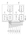
Since the storing modules M1˜Mn comprise the same circuit structures, only the storing modules M1 and M2 are shown in FIG. 2. FIG. 2 is a schematic diagram of an exemplary embodiment of a storage medium. The storing module M1 comprises a controller 211 and a memory cell 212. The storing module M2 comprises a controller 221 and a memory cell 222. The controller 211 accesses the memory cell 212. The controller 221 accesses the memory cell 222. In one embodiment, the memory cells 212 and 222 are independent of NAND flash memories. Thus, the memory cells 212 and 222 are accessed by a single controller.
In this embodiment, the storing module M1 comprises an ECC engine 213 and the storing module M2 comprises an ECC engine 223. The ECC engine 213 corrects the data received by the controller 211. The ECC engine 223 corrects the data received by the controller 221.
Taking the ECC engine 213 as an example, the controller 211 reads data stored in the memory cell 212 to generate an accessing result and provides the accessing result to the ECC engine 213 to correct errors. The ECC engine 213 corrects the accessing result to generate a corrected result and provides the corrected result to the controller 211. In one embodiment, the ECC engine 213 is integrated in the controller 211.
During a read cycle, when the storing module M1 is a main module, the controller 211 reads the memory cell 212 to generate a first accessing result according to address information. The controller 211 utilizes the ECC engine 213 to execute an ECC operation for the first accessing result. When the first accessing result does not have an error or the first accessing result has an error and the error can be corrected, the controller 211 corrects the first accessing result to generate corrected data, serves the corrected data as read data and provides the read data to the host device 110 via the transmittal lines DAT0˜DAT3.
However, if the first accessing result has various error bits, the first accessing result cannot be corrected. The storing module M1 requests the storing module M2 to serve as a main module. In this embodiment, the controller 221 reads the memory cell 222 to generate a second accessing result and utilizes the ECC engine 223 to execute an ECC operation for the second accessing result. When the second accessing result does not have an error or the second accessing result has an error and the error can be corrected, the controller 221 corrects the second accessing result to generate corrected data, serves the corrected data as read data and provides the read data to the host device 110 via the transmittal lines DAT0˜DAT3.
In another embodiment, when the controller 211 cannot provide correction data to the host device 110, the controller 221 is utilized to provide data to the host device 110 according to address information. The controller 211 stores the data, which is provided by the controller 221, to the memory cell 212 according to the address information. Thus, the storing module M1 may serve as a main module again or serve as a sub-module.
FIG. 3 is a flow chart of an exemplary embodiment of an access method. The access method is applied to a storage medium. Taking FIG. 2 as an example, the storage medium comprises a first module M1 and a second module M2. The first module M1 comprises a first controller 211 and a first memory cell 212. The second module M2 comprises a second controller 221 and a second memory cell 222. In this embodiment, assume that the first module M1 is a main module and the second module M2 is a sub-module.
First, a read command is received (step 311). In one embodiment, the read command is sent from a host device. In this embodiment, since the first module M1 is a main module, the first controller 211 reads data stored in the first memory cell 212 to generate a first accessing result according to address information of the read command.
It is determined whether the first accessing result has an error and whether the error can be corrected (step 312). When the first accessing result has an error and the error cannot be corrected, the second module M2 is read to generate a second accessing result and the second accessing result serves as read data (step 313). In this embodiment, when the first module M1 cannot provide data, the first controller 211 requests the second controller 221 to read the second memory cell 222. Thus, the second controller 221 reads the second memory cell 222 to generate a second accessing result according to the address information of the read command.
The invention does not limit the kind of the protocol between the first and the second controllers. The first controller 211 communicates with the second controller 221 according to an SD protocol, an I2C protocol or an UART protocol.
When the error of the first accessing result can be corrected, the corrected accessing result serves as read data (step 314). Final, the read data is provided to a host device (step 315). In one embodiment, when the first accessing result has an error and the error cannot be corrected, the second accessing result is stored in the first memory cell according to address information.
FIG. 4 is a flow chart of another exemplary embodiment of the access method. During a write cycle, write data is received (step 411). In one embodiment, the write data is provided by a host device. Referring to FIG. 2, the write data is stored in the first module M1 and the second module M2.
It is determined whether the first module M1 and the second module M2 are idle (step 412). In this embodiment, since the first module M1 is a main module, the first module M1 determines whether the second module M2 has completed a writing operation, which stores the write data in the memory cell 222. In one embodiment, the first module M1 determines whether the second module M2 has completed the writing operation according to the levels of the transmittal lines DAT1 and DAT2 of an SD protocol.
When the first module M1 and the second module M2 are idle, it represents that each of the first module M1 and the second module M2 has completed the writing operation. Thus, a finish response is sent to the host device (step 415) and the writing operation is ended (step 416). In this embodiment, the first module M1 sends the finish response to the host device. In one embodiment, when the first module M1 and the second module M2 complete the writing operation, the first module M1 sets the level of the transmittal line DAT0 to a high level.
When the first module M1 or the second module M2 is not idle, it represents that one of the first module M1 and the second module M2 has not completed the writing operation. Thus, an unfinished response is sent to the host device (step 413). In this embodiment, when one of the first module M1 or the second module M2 has not completed the writing operation, the first module M1 sets the level of the transmittal line DAT0 to a low level and the first module M1 or the second module M2 continuously stores the write data (step 414).
FIG. 5 is a flowchart of another exemplary embodiment of an access method. First, an asking command is received (step 511). In this embodiment, a host device sends the asking command. Before executing a writing operation and a read operation, the host device sends an asking command to a storage medium.
It is determined whether the storage medium is ready (step 512). In this embodiment, the first module M1 serves as a main module such that the first module M1 determines whether the module M2 is ready via the transmittal lines DAT1 and DAT2. In one embodiment, the first module M1 comprises an operating conditions register (OCR). The OCR has a busy bit, which is referred to as a card power-up status bit. When the busy bit is 1, it represents that the first module M1 and the second module M2 are ready. When the busy bit is 0, it represents that the first module M1 or the second module M2 is not ready. After all modules are ready, the first module M1 sets the busy bit to 1. The host device reads the busy bit of the OCR of the first module M1 to determine whether the first module M1 and the second module M2 are ready.
When the first module M1 and the second module M2 are ready, a ready response is sent to the host device (step 513) and the initiate operation is ended (step 514). In this embodiment, the ready response sets the busy bit of the OCR to 1. In another embodiment, the first module M1 communicates with the second module M2 via the transmittal lines DAT1 and DAT2.
When the first module M1 or the second module M2 is not ready, an unready response is generated (step 515) and sent to the host device (step 516). In this embodiment, step 515 sets the busy bit of the OCR of the first module M1 to 0, and step 516 provides all bit statuses of the OCR to the host device. The host device determines that the first module M1 or the second module M2 is not ready according to the busy bit of the OCR and sends an asking command to the storage medium until the first module M1 and the second module M2 are ready.
FIG. 6 is a flowchart of an exemplary embodiment of an access method. In this embodiment, assuming that the storage medium is an SD card. First, an SD command is received (step 611). In other embodiments, a host device sends a corresponding command to initial the storage medium according to the kind of the storage medium.
Next, it is determined whether the storage medium is idle (step 612). In this embodiment, the first module M1 determines whether the second module M2 is idle via the transmittal lines DAT1 and DAT2. When the first module M1 and the second module M2 are idle, an idle response is sent to the host device (step 613). In one embodiment, the first module M1 sets the level of the transmittal line DAT0 to an idle level, such as a high level. The host device determines that the storage medium is idle according to the level of the transmittal line DAT0.
When the first module M1 or the second module M2 is not idle, a non-idle response is sent to the host device (step 614) and step 612 is executed to determine whether the first module M1 and the second module M2 are ready. In this embodiment, the first module M1 sets the level of the transmittal line DAT0 to a busy level, such as a low level.
Since the storage medium comprises a plurality of storing modules and each storing module stores the same data, when a host device desires to access the storage medium, a main storing module among the storing modules communicates with the host device and the other storing modules. The main storing module stores data and provides a portion of the data to the host device. When the main storing module provides the data to the host device, if the data has many incorrect bits and the main storing module cannot correct the incorrect bits, another storing module is selected to communicate with the host device. Thus, the host device can normally execute an accessing operation.
Unless otherwise defined, all terms (including technical and scientific terms) used herein have the same meaning as commonly understood by one of ordinary skill in the art to which this invention belongs. It will be further understood that terms, such as those defined in commonly used dictionaries, should be interpreted as having a meaning that is consistent with their meaning in the context of the relevant art and will not be interpreted in an idealized or overly formal sense unless expressly so defined herein.
While the invention has been described by way of example and in terms of the preferred embodiments, it is to be understood that the invention is not limited to the disclosed embodiments. To the contrary, it is intended to cover various modifications and similar arrangements (as would be apparent to those skilled in the art). Therefore, the scope of the appended claims should be accorded the broadest interpretation so as to encompass all such modifications and similar arrangements.

Claims (16)

What is claimed is:
1. A storage medium receiving write data provided by a host device and providing read data to the host, comprising:
a first module comprising:
a first memory cell storing the write data;
a first controller reading the first memory cell to generate a first accessing result; and
a second module comprising:
a second memory cell storing the write data; and
a second controller reading the second memory cell,
wherein when the first accessing result has an error and the error cannot be corrected by the first controller, the first controller requests the second controller to read the second memory cell to generate a second accessing result, and the second controller serves the second accessing result as the read data and provides the read data to the host; and
wherein after the second controller has written the write data to the second memory cell, the first controller sends a response signal to the host device.
2. The storage medium as claimed in claim 1, wherein when the error can be corrected by the first controller, the first controller corrects the first accessing data to generate corrected data and serves the corrected data as the read data.
3. The storage medium as claimed in claim 1, wherein when the error cannot be corrected, the second controller reads the second memory cell according to address information to generate the second accessing result, and the first controller stores the second accessing result to the first memory cell according to the address information.
4. The storage medium as claimed in claim 1, wherein during a write cycle, the first and the second controllers write the write data to the first and the second memory cells respectively and the first controller confirms whether the second controller has written the write data to the second memory cell.
5. The storage medium as claimed in claim 1, wherein the first controller communicates with the second controller according to a secure digital (SD) protocol, an inter-integrated circuit (I2C) protocol or an universal asynchronous receiver transmitter (UART) protocol.
6. An access system comprising:
a host device providing write data or receiving read data; and
a storage medium communicating with the host device and comprising:
a first module comprising:
a first memory cell storing the write data; and
a first controller reading the first memory cell to generate a first accessing result; and
a second module comprising:
a second memory cell storing the write data; and
a second controller reading the second memory cell,
wherein when the first accessing result has an error and the error cannot be corrected by the first controller, the first controller requests the second controller to read the second memory cell to generate a second accessing result, and the second controller serves the second accessing result as the read data and provides the read data to the host device; and
wherein after the second controller has written the write data to the second memory cell, the first controller sends a response signal to the host device.
7. The access system as claimed in claim 6, wherein when the error can be corrected by the first controller, the first controller corrects the first controller to generate corrected data and serves the corrected data as the read data.
8. The access system as claimed in claim 6, wherein when the error cannot be corrected, the second controller reads the second memory cell according to address information to generate the second accessing result, and the first controller stores the second accessing result to the first memory cell according to the address information.
9. The access system as claimed in claim 6, wherein during a write cycle, the first and the second controllers write the write data to the first and the second memory cells and the first controller confirms whether the second controller has written the write data to the second memory cell.
10. The access system as claimed in claim 6, wherein the first controller communicates with the second controller according to a secure digital (SD) protocol, an inter-integrated circuit (I2C) protocol or an universal asynchronous receiver transmitter (UART) protocol.
11. An access method for a storage medium comprising a first module and a second module, wherein the first module comprises a first controller and a first memory cell, and the second module comprises a second controller and a second memory cell, comprising:
activating the first controller to receive a read command;
reading the first memory cell to generate a first accessing result according to the read command;
requesting the second controller to read the second memory cell to generate a second accessing result and serving the second accessing result as read data when the first accessing result has an error and the error cannot be corrected; and
providing the read data to a host device, wherein after the second controller has written write data to the second memory cell, the first controller sends a response signal to the host device.
12. The access method as claimed in claim 11, further comprising:
correcting the first accessing result to generate corrected data and serving the corrected data as the read data when the error can be corrected.
13. The access method as claimed in claim 11, further comprising:
reading the second memory cell to generate the second accessing result according to address information.
14. The access method as claimed in claim 11, further comprising:
storing the second accessing result to the first memory cell according to the address information when the error cannot be corrected.
15. The access method as claimed in claim 11, wherein the step of requesting the second controller to read the second memory cell is executed by the first controller.
16. The access method as claimed in claim 15, wherein the first controller communicates with the second controller according to a secure digital (SD) protocol, an inter-integrated circuit (I2C) protocol or an universal asynchronous receiver transmitter (UART) protocol.
US13/947,979 2012-11-12 2013-07-22 Storage medium, system and method utilizing the same Active 2033-09-18 US9009571B2 (en)

Applications Claiming Priority (3)

Application Number Priority Date Filing Date Title
TW101141990A TWI557636B (en) 2012-11-12 2012-11-12 Storage medium, accessing system and accessing method thereof
TW101141990 2012-11-12
TW101141990A 2012-11-12

Publications (2)

Publication Number Publication Date
US20140136929A1 US20140136929A1 (en) 2014-05-15
US9009571B2 true US9009571B2 (en) 2015-04-14

Family

ID=50682945

Family Applications (1)

Application Number Title Priority Date Filing Date
US13/947,979 Active 2033-09-18 US9009571B2 (en) 2012-11-12 2013-07-22 Storage medium, system and method utilizing the same

Country Status (3)

Country Link
US (1) US9009571B2 (en)
CN (2) CN103809918A (en)
TW (1) TWI557636B (en)

Cited By (1)

* Cited by examiner, † Cited by third party
Publication number Priority date Publication date Assignee Title
US20150199223A1 (en) * 2014-01-14 2015-07-16 Nvidia Corporation Approach to predictive verification of write integrity in a memory driver

Families Citing this family (3)

* Cited by examiner, † Cited by third party
Publication number Priority date Publication date Assignee Title
KR20200110009A (en) * 2019-03-15 2020-09-23 코웨이 주식회사 Method for Recover an Error of Control Module of Multi-Function Storage System
KR20210050304A (en) * 2019-10-28 2021-05-07 에스케이하이닉스 주식회사 Memory device and operating method thereof
US11783866B2 (en) * 2021-06-02 2023-10-10 Western Digital Technologies, Inc. Data storage device and method for legitimized data transfer

Citations (7)

* Cited by examiner, † Cited by third party
Publication number Priority date Publication date Assignee Title
US20060212656A1 (en) 2005-03-17 2006-09-21 Fujitsu Limited Dual storage apparatus and control method for the dual storage apparatus
US20060288177A1 (en) * 2005-06-21 2006-12-21 Mark Shaw Memory mirroring apparatus and method
US20070255999A1 (en) * 2006-04-07 2007-11-01 Qimonda Ag Memory Arrangement And Method For Error Correction
US20080010435A1 (en) * 2005-06-24 2008-01-10 Michael John Sebastian Smith Memory systems and memory modules
US20110047440A1 (en) * 2009-08-24 2011-02-24 International Business Machines Corporation Systems and Methods to Respond to Error Detection
TW201133498A (en) 2010-03-22 2011-10-01 Phison Electronics Corp Error correcting method, and memory controller and memory storage system using the same
US20120110414A1 (en) * 2006-04-26 2012-05-03 Qimonda Ag Memory-Module Controller, Memory Controller and Corresponding Memory Arrangement, and Also Method for Error Correction

Family Cites Families (2)

* Cited by examiner, † Cited by third party
Publication number Priority date Publication date Assignee Title
CN100409164C (en) * 2003-07-07 2008-08-06 日立超大规模集成电路系统株式会社 Storage device and storage system
US7307902B2 (en) * 2005-08-30 2007-12-11 Hewlett-Packard Development Company, L.P. Memory correction system and method

Patent Citations (10)

* Cited by examiner, † Cited by third party
Publication number Priority date Publication date Assignee Title
US20060212656A1 (en) 2005-03-17 2006-09-21 Fujitsu Limited Dual storage apparatus and control method for the dual storage apparatus
US20060288177A1 (en) * 2005-06-21 2006-12-21 Mark Shaw Memory mirroring apparatus and method
US20080010435A1 (en) * 2005-06-24 2008-01-10 Michael John Sebastian Smith Memory systems and memory modules
US20070255999A1 (en) * 2006-04-07 2007-11-01 Qimonda Ag Memory Arrangement And Method For Error Correction
US20120110414A1 (en) * 2006-04-26 2012-05-03 Qimonda Ag Memory-Module Controller, Memory Controller and Corresponding Memory Arrangement, and Also Method for Error Correction
US8250436B2 (en) * 2006-04-26 2012-08-21 Qimonda Ag Memory-module controller, memory controller and corresponding memory arrangement and also method for error correction
US20110047440A1 (en) * 2009-08-24 2011-02-24 International Business Machines Corporation Systems and Methods to Respond to Error Detection
US8572455B2 (en) * 2009-08-24 2013-10-29 International Business Machines Corporation Systems and methods to respond to error detection
TW201133498A (en) 2010-03-22 2011-10-01 Phison Electronics Corp Error correcting method, and memory controller and memory storage system using the same
US8386905B2 (en) 2010-03-22 2013-02-26 Phison Electronics Corp. Error correcting method, and memory controller and memory storage system using the same

Non-Patent Citations (1)

* Cited by examiner, † Cited by third party
Title
English language machine translation of TW 201133498 (published Oct. 11, 2011).

Cited By (2)

* Cited by examiner, † Cited by third party
Publication number Priority date Publication date Assignee Title
US20150199223A1 (en) * 2014-01-14 2015-07-16 Nvidia Corporation Approach to predictive verification of write integrity in a memory driver
US9411668B2 (en) * 2014-01-14 2016-08-09 Nvidia Corporation Approach to predictive verification of write integrity in a memory driver

Also Published As

Publication number Publication date
TWI557636B (en) 2016-11-11
CN103809918A (en) 2014-05-21
US20140136929A1 (en) 2014-05-15
CN108920299B (en) 2022-05-24
CN108920299A (en) 2018-11-30
TW201419127A (en) 2014-05-16

Similar Documents

Publication Publication Date Title
CN101576853B (en) Data access method and controller and memory system using same
CN107122317B (en) Data storage device
US20190266096A1 (en) Data storage device, method of operating the same, and storage system having the same
US8423838B2 (en) Block management method, memory controller, and memory storage apparatus
US20180239557A1 (en) Nonvolatile memory device, data storage device including the same, and operating method of data storage device
US11704048B2 (en) Electronic device
US8301981B2 (en) Data access method for flash memory and storage system and controller thereof
US9009571B2 (en) Storage medium, system and method utilizing the same
US20120166706A1 (en) Data management method, memory controller and embedded memory storage apparatus using the same
US10546618B2 (en) Nonvolatile memory device, data storage device including the same and operating method thereof
US10754768B2 (en) Memory system using descriptor lookup tables to access setting information for a non-volatile memory, and an operating method thereof
US11748025B2 (en) Nonvolatile memory device, data storage device including the same and operating method thereof
US20190236020A1 (en) Memory system and operating method thereof
KR102645786B1 (en) Controller, memory system and operating method thereof
CN102543184B (en) Memorizer memory devices, its Memory Controller and method for writing data
US11720276B2 (en) Memory system and controller for managing write status
US11593285B2 (en) Memory system
US11366736B2 (en) Memory system using SRAM with flag information to identify unmapped addresses
US10564896B2 (en) Data storage device and operating method thereof
CN114579484A (en) Data storage device and method of operating the same
US20190179749A1 (en) Memory system, operating method thereof and nonvolatile memory device
US10203891B2 (en) Data storage device and data processing system
US9111586B2 (en) Storage medium and transmittal system utilizing the same
CN106940623B (en) Memory management method, memory control circuit unit and memory storage device
CN115048051A (en) Data reading method, memory controller and memory storage device

Legal Events

Date Code Title Description
AS Assignment

Owner name: SILICON MOTION, INC., TAIWAN

Free format text: ASSIGNMENT OF ASSIGNORS INTEREST;ASSIGNORS:LIU, CHENG-WEI;OU, HSU-PING;SIGNING DATES FROM 20130715 TO 20130717;REEL/FRAME:030850/0772

STCF Information on status: patent grant

Free format text: PATENTED CASE

MAFP Maintenance fee payment

Free format text: PAYMENT OF MAINTENANCE FEE, 4TH YEAR, LARGE ENTITY (ORIGINAL EVENT CODE: M1551)

Year of fee payment: 4

MAFP Maintenance fee payment

Free format text: PAYMENT OF MAINTENANCE FEE, 8TH YEAR, LARGE ENTITY (ORIGINAL EVENT CODE: M1552); ENTITY STATUS OF PATENT OWNER: LARGE ENTITY

Year of fee payment: 8