BACKGROUND OF THE INVENTION
1. Field of the Invention
The present invention generally relates to a transient-to-digital convertor, and more particularly to a transient-to-digital convertor generating digital codes according to an electrostatic discharge (ESD) pulse.
2. Description of Related Art
An electrostatic discharge (ESD) event is an important reliability issue for integrated circuits (ICs). ESD protection is also a critical reliability issue for ICs. As semiconductor processes advance toward deep sub-micron manufacturing, scaled-down devices and thinner gate oxides are more vulnerable to ESD stress. Generally, the IC chips must have the ability to withstand certain levels of ESD of high stress in machine mode (MM) or in human body mode (HBM). The issues result from strict reliability test standard requirements, such as system-level ESD tests.
The additional noise filter networks, such as the decoupling capacitor, transient voltage suppressor (TVS), and/or current-limiting resistance, are often used to improve the system-level ESD immunity of microelectronic products. The system-level ESD immunity of CMOS ICs under system-level ESD test can be significantly enhanced by choosing proper noise filter networks. However, the additional discrete noise-bypassing components substantially increase the total cost of microelectronic products. Therefore, a need has arisen by IC industry to propose a novel chip-level solution which meets high system-level ESD specification for microelectronic products without additional discrete noise-decoupling components on the microelectronic products.
SUMMARY OF THE INVENTION
In view of the foregoing, it is an object of the present invention to provide an on-chip transient-to-digital convertor which outputs digital codes corresponding to different ESD voltages without additional discrete noise-bypassing components, and executes an auto-recovery procedure in microelectronic systems based on RC delay effect after detecting an ESD pulse, which achieves decreased cost.
According to one embodiment, a self-reset transient-to-digital convertor which includes at least one transient detection circuit is disclosed. The transient detection circuit, coupled between a first power line and a second power line, includes at least one voltage drop unit, a current amplifier unit, and a time control unit. When an ESD event occurs, the voltage drop unit is conducted to pass through an ESD current. The current amplifier unit, coupled between the voltage drop unit and a first node, is conducted by the ESD current to set the level of the first node. The time control unit, coupled between the first node and the second power line, is configured to gradually drain the ESD current away. Wherein, each of the transient detection circuit generates a digital code according to the level of the first node.
According to another embodiment, an electronic product which includes at least one transient-to-digital convertor is disclosed. The transient-to-digital convertor includes at least one transient detection circuit which is coupled between a first power line and a second power line. The transient detection circuit includes at least one voltage drop unit, a current amplifier unit, and a time control unit. When an ESD event occurs, the voltage drop unit is conducted to pass through an ESD current. The current amplifier unit, coupled between the voltage drop unit and a first node, is conducted by the ESD current to set the level of the first node. The time control unit, coupled between the first node and the second power line, is configured to gradually drain the ESD current away. Wherein, each of the transient detection circuit generates a digital code according to the level of the first node.
BRIEF DESCRIPTION OF THE DRAWINGS
FIG. 1 illustrates an electronic product according to one embodiment of the present invention;
FIG. 2 illustrates a transient-to-digital convertor according to one embodiment of the present invention;
FIG. 3 illustrates a transient detection circuit according to one embodiment of the present invention;
FIG. 4 illustrates a 3-bit transient-to-digital convertor according to one embodiment of the present invention; and
FIGS. 5 a-5 c illustrate the digital codes according to one embodiment of the present invention.
DETAILED DESCRIPTION OF THE INVENTION
Firstly, FIG. 1 illustrates an electronic product 1 according to one embodiment of the present invention. As shown in FIG. 1, the electronic product 1 includes a plurality of internal circuits 11 a-11 n, a plurality of transient-to-digital convertors 13 a-13 n, and a processor 15. The transient-to-digital convertors 13 a-13 n, coupled with the internal circuits 11 a-11 n respectively, are configured to detect whether an ESD event occurs in the internal circuits 11 a-11 n and accordingly generate the digital code VOUT. In one embodiment, the transient-to-digital convertors 13 a-13 n may be integrated in the CMOS chips of the internal circuits 11 a-11 n. The processor 15, coupled to the transient-to-digital convertors 13 a-13 n, receives the generated digital code VOUT to determine whether the ESD event occurs in the corresponding internal circuits 11 a-11 n. Specifically, the internal circuits 11 a-11 n may be single chips, timing controllers, driving circuits, or the combination thereof.
Afterwards, FIG. 2 illustrates a transient-to-digital convertor according to one embodiment of the present invention. Taking the transient-to-digital convertor 13 a for example, it includes a plurality of transient detection circuits 13 a 1-13 an, and each of them couples between a first power line (voltage source VDD) 21 and a second power line (ground VSS) 23. When an ESD event occurs in the first power line 21, the transient detection circuits 13 a 1-13 an generate digital codes VOUT1-VOUTN according to amplitude of an ESD pulse generated by the ESD event.
FIG. 3 illustrates a transient detection circuit according to one embodiment of the present invention. Taking the transient detection circuit 13 a 1 for example, it includes a voltage drop unit 13 a 11, a current amplifier unit 13 a 13, a time control unit 13 a 15, and a buffer unit 13 a 17. When the ESD event occurs in the first power line 21, the voltage drop unit 13 a 11 is conducted to pass through an ESD current. The current amplifier unit 13 a 13, coupled between the voltage drop unit 13 a 11 and a first node A, is conducted by the ESD current to set the level of the first node A. In one embodiment, the voltage drop unit 13 a 11 includes two diodes connected to which in serial. The current amplifier unit 13 a 13 includes a first transistor M1 and a second transistor M2, wherein the first transistor M1 is coupled between the voltage drop unit 13 a 11 and the second power line 23, and the second transistor M2 is coupled between the first power line 21 and the first node A. The gate of the second transistor M2 is connected to the gate of the first transistor M1. The voltage drop unit 13 a 11 may be configured between the current amplifier unit 13 a 13 and the first power line 21, and/or between the current amplifier unit 13 a 13 and the second power line 23.
Assume that the level of the first node A is 0 (low level) in regular operation (no ESD event occurs). Once the ESD voltage generated by the ESD event is large enough to conduct the diodes of the voltage drop unit 13 a 11, the second transistor M2 is activated, so that the ESD current is directed into the first node A to change the level of the first node A from 0 (low level) to 1 (high level).
The time control unit 13 a 15, coupled between the first node A and the second power line 23, includes a resistor R and a capacitor C, where the resistor R is coupled between the first node A and the second power line 23, and the capacitor C is connected to the resistor R in parallel. At first, the capacitor C of the time control unit 13 a 15 may be charged because the ESD current is directed into the first node A, so as to change the level of the first node A from 0 to 1. Then, based on the nature delay time constant of RC circuits, the resistor R can gradually drain the ESD current to the second power line 23, so as to reset the level of the first node A to 0 automatically.
A user can obtain, whether an ESD event occurs according to the level of the first node A. Alternatively, in this embodiment, the buffer unit 13 a 17, coupled to the first node A, can be used to process the level of the first node A for increasing the driving function of the level of the first node A. The processed result serves as a digital code VOUT1. Specifically, the buffer unit 13 a 17 includes an inverter for inverting the level of the first node A and providing the inverted result to serve as the digital code VOUT1. In another embodiment, the buffer unit 13 a 17 may include several inverters or be omitted.
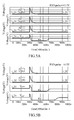
The transient-to-digital convertor 13 a having only one transient detection circuit 13 a 1 (1-bit transient-to-digital convertor) merely can indicate or warn whether an ESD event occurs. In some cases, plural transient detection circuits may be configured in the transient-to-digital convertor 13 a to determine the level of the ESD pulse generated by the ESD event. FIG. 4 illustrates a 3-bit transient-to-digital convertor according to one embodiment of the present invention. As shown in FIG. 4, the transient-to-digital convertor 13 a includes three transient detection circuits 13 a 1-13 a 3 with different ESD abilities, respectively. The digital codes outputted by the transient-to-digital convertor 13 a correspond to different ESD voltages. Specifically, the voltage drop unit 13 a 11-13 a 31 in the transient detection circuits 13 a 1-13 a 3 have two, three, and four diodes, respectively, for withstanding different amplitudes of the ESD pulse. For example, when the amplitude of the ESD pulse is 3.5V, only the voltage drop unit 13 a 11 is conducted, so that the level of the digital code VOUT1 is changed to 0, and the levels of the digital codes VOUT2, VOUT3 are still 1, as shown in FIG. 5A, the digital codes outputted by the transient-to-digital convertor 13 a can be referred to as “110.” Based on delay time constant, the resistor IR of the time control unit 13 a 15 then gradually drains the ESD current at the first node A away to reset the level of the first node A to 0 automatically, so as to operate with regular voltage.
Similarly, if generating more ESD pulse such as 4.5V which is large enough to conduct the three diodes of the voltage drop unit 13 a 21, the levels of the digital codes VOUT1, VOUT2 are changed to 0, and the level of the digital code VOUT3 is still 1, as shown in FIG. 5B, the digital codes outputted by the transient-to-digital convertor 13 a can be referred to as “100.” Based on delay time constant, the resistors R of the time control units 13 a 15, 13 a 25 then gradually drain the ESD current at the first nodes A away respectively, so as to reset the levels of the first nodes A to 0 automatically. If further generating more ESD pulse such as 5.5V which is large enough to conduct the four diodes of the voltage drop unit 13 a 31, the levels of all the digital codes VOUT1-VOUT3 are changed to 0, as shown in FIG. 5C, the digital codes outputted by the transient-to-digital convertor 13 a can be referred to as “000.” The time control units 13 a 15-13 a 35 then drain the ESD current at the first nodes A away respectively, so as to operate with regular voltage. Due to the factor that the number of the diodes included in the voltage drop units 13 a 11-13 a 31 of the transient-to-digital convertor 13 a is directly proportional to the detected ESD pulse, so the outputted digital codes can be used to determine the level of the ESD pulse generated by the ISD event.
The processor 15 receives the generated digital codes VOUT1-VOUT3 and accordingly to execute a specific action. Specifically, by providing a hardware/firmware co-design, it indicates that the ESD pulse generated by the ESD event exceeds a preset value when the level of the digital codes VOUT3 is changed to 0, then the processor 15 executes total system auto-recovery for the internal circuit where that ESD event occurs. In opposition, it indicates that the ESD pulse generated by the ESD event is smaller than the preset value if only the level of the digital codes VOUT1 is changed to 0, the processor 15 executes partial system auto-recovery for the internal circuit where that ESD event occurs. Therefore, the hardware/firmware co-design with the transient-to-digital convertor 13 a can improve the immunity of CMOS IC products against electrical transient disturbance.
According to the above embodiment, the self-reset transient-to-digital convertor and electronic product utilizing the same, provided in the present invention, convert the transient voltage into the digital codes to detect whether an ESD event occurs. Therefore, when the ESD event occurs, it can issue a protect/warn signal without additional discrete noise-bypassing components. Furthermore, the present invention utilizes plural transient detection circuits with different level of converting to determine the level of the ESD pulse generated by the ESD event according to the outputted digital codes. The present invention also bypasses transient voltages or currents by RC circuit to reset to regular voltage automatically. So that the traditional reset hardware/firmware may be omitted, which achieves decreased cost.
Although specific embodiments have been illustrated and described, it will be appreciated by those skilled in the art that various modifications may be made without departing from the scope of the present invention, which is intended to be limited solely by the appended claims.