US8994122B2 - Semiconductor device having a memory cell region and a peripheral transistor region - Google Patents
Semiconductor device having a memory cell region and a peripheral transistor region Download PDFInfo
- Publication number
- US8994122B2 US8994122B2 US13/785,494 US201313785494A US8994122B2 US 8994122 B2 US8994122 B2 US 8994122B2 US 201313785494 A US201313785494 A US 201313785494A US 8994122 B2 US8994122 B2 US 8994122B2
- Authority
- US
- United States
- Prior art keywords
- film
- gate
- conductor
- insulating film
- region
- Prior art date
- Legal status (The legal status is an assumption and is not a legal conclusion. Google has not performed a legal analysis and makes no representation as to the accuracy of the status listed.)
- Active
Links
Images


Classifications
-
- H01L29/4925—
-
- H—ELECTRICITY
- H10—SEMICONDUCTOR DEVICES; ELECTRIC SOLID-STATE DEVICES NOT OTHERWISE PROVIDED FOR
- H10D—INORGANIC ELECTRIC SEMICONDUCTOR DEVICES
- H10D64/00—Electrodes of devices having potential barriers
- H10D64/60—Electrodes characterised by their materials
- H10D64/66—Electrodes having a conductor capacitively coupled to a semiconductor by an insulator, e.g. MIS electrodes
- H10D64/661—Electrodes having a conductor capacitively coupled to a semiconductor by an insulator, e.g. MIS electrodes the conductor comprising a layer of silicon contacting the insulator, e.g. polysilicon having vertical doping variation
- H10D64/662—Electrodes having a conductor capacitively coupled to a semiconductor by an insulator, e.g. MIS electrodes the conductor comprising a layer of silicon contacting the insulator, e.g. polysilicon having vertical doping variation the conductor further comprising additional layers, e.g. multiple silicon layers having different crystal structures
-
- H01L27/10829—
-
- H01L27/10885—
-
- H01L27/10888—
-
- H—ELECTRICITY
- H10—SEMICONDUCTOR DEVICES; ELECTRIC SOLID-STATE DEVICES NOT OTHERWISE PROVIDED FOR
- H10B—ELECTRONIC MEMORY DEVICES
- H10B12/00—Dynamic random access memory [DRAM] devices
- H10B12/30—DRAM devices comprising one-transistor - one-capacitor [1T-1C] memory cells
- H10B12/37—DRAM devices comprising one-transistor - one-capacitor [1T-1C] memory cells the capacitor being at least partially in a trench in the substrate
-
- H—ELECTRICITY
- H10—SEMICONDUCTOR DEVICES; ELECTRIC SOLID-STATE DEVICES NOT OTHERWISE PROVIDED FOR
- H10B—ELECTRONIC MEMORY DEVICES
- H10B12/00—Dynamic random access memory [DRAM] devices
- H10B12/30—DRAM devices comprising one-transistor - one-capacitor [1T-1C] memory cells
- H10B12/48—Data lines or contacts therefor
- H10B12/482—Bit lines
-
- H—ELECTRICITY
- H10—SEMICONDUCTOR DEVICES; ELECTRIC SOLID-STATE DEVICES NOT OTHERWISE PROVIDED FOR
- H10B—ELECTRONIC MEMORY DEVICES
- H10B12/00—Dynamic random access memory [DRAM] devices
- H10B12/30—DRAM devices comprising one-transistor - one-capacitor [1T-1C] memory cells
- H10B12/48—Data lines or contacts therefor
- H10B12/485—Bit line contacts
Definitions
- This invention relates to a semiconductor device.
- Patent Document 1 discloses a planar transistor which is designed to realize a large work function by segregating halogens on an interface between a gate insulating film including a high-k film formed on a semiconductor substrate and a metal gate film formed on the gate insulating film.
- Patent Document 2 discloses a technique for forming a high-performance and low-voltage metal-insulator-semiconductor field effect transistor (MISFE) by using a damascene process to form a gate insulating film including a high-k film and a metal gate film without exposing the gate insulating film and the metal gate film to annealing for activation of source and drain regions.
- MISFE metal-insulator-semiconductor field effect transistor
- an embedded gate transistor in which a gate insulating film is formed on the inner walls of a trench for gate electrode formed in the surface of a semiconductor substrate, and a gate electrode is embedded in the trench surrounded by the gate insulating film.
- Patent Document 3 discloses an embedded gate transistor which is designed to suppress reduction of effective electric field and increase of threshold voltage by forming a gate insulating film on inner walls of a trench for gate electrode such that the gate insulating film has a smaller thickness at the corners of the trench bottom at least than the thickness of the film on the side walls of the trench.
- an embedded gate transistor is used in a memory cell region while a planar transistor having a gate insulating film including a high-k film is used in a peripheral transistor region.
- the inventors of this invention have reviewed a DRAM having the aforementioned configuration and the manufacturing method thereof, and results obtained will be described with reference to FIGS. 18 to 29 .
- a DRAM (semiconductor device) 300 has a memory cell region 300 a and a peripheral transistor region 300 b .
- the memory cell region 300 a and the peripheral transistor region 300 b are divided into a plurality of active regions 11 a , 11 b , 11 c by STIs (Shallow Trench Isolations) 12 formed in a semiconductor substrate 10 .
- STIs Shallow Trench Isolations
- peripheral transistor region 300 b There are respectively formed, in the active regions 11 b and 11 c of the peripheral transistor region 300 b , n-channel and p-channel planar transistors (hereafter, referred to as the peripheral transistors) each having a gate insulating film including a high-k film.
- a manufacturing method of the DRAM 300 will be described with reference to FIGS. 19 to 29 .
- STIs 12 for defining the active regions 11 a , 11 b , and 11 c are formed in a semiconductor substrate 10 formed of a p-type silicon substrate. Then, an insulating film 16 is formed to cover the top faces of the STIs 12 and the semiconductor substrate 10
- embedded gate transistors are formed in the active region 11 a of the memory cell region 300 a .
- Each of the embedded gate transistors for memory cells has a gate insulating film 18 , a gate electrode 20 , an insulating film 23 , and impurity diffusion regions 14 a , 14 b.
- a silicon oxide film 26 ′ is formed on the structure shown in FIG. 20 .
- the silicon oxide film 26 ′ on the peripheral transistor region 300 b is removed, whereby a first interlayer insulating film 26 is formed in the memory cell region 300 a.
- a high-k film 28 ′ is formed to cover the first interlayer insulating film 26 and the insulating film 16 in the peripheral transistor region 300 b.
- a metal film and a doped polysilicon film are sequentially stacked on the structure shown in FIG. 23 , and the stacked films are patterned.
- a metal gate film 30 and an upper gate film 32 are formed in each of the active regions 11 b , 11 c of the peripheral transistor region 300 b .
- the height from the semiconductor substrate 10 to the top face of the metal gate film 30 sometimes becomes higher than the height from the semiconductor substrate 10 to the top face of the first interlayer insulating film 26 .
- the height b of the top face of the upper gate film 32 sometimes becomes higher than the height A of the top face of the first interlayer insulating film 26 .
- the high-k film 28 ′ in the memory cell region 300 a and the peripheral transistor region 300 b except the one under the metal gate film 30 are removed.
- a gate insulating film 28 including a high-k film is formed in each of the active regions 11 b , 11 c of the peripheral transistor region 300 b.
- bit contact holes 27 are formed in the first interlayer insulating film 26 .
- a first interlayer insulating film 26 is formed to fill the bit contact holes 27 while a fifth conductor film 39 is formed to cover the upper gate film 32 .
- a sixth conductor film 43 is stacked on the fifth conductor film 39 .
- the height of the top face of the upper gate film 32 is higher than the height of the top face of the first interlayer insulating film 26 , there is generated a difference in level between the top face of the fifth conductor film 39 and the top face of the sixth conductor film 43 .
- CMP Chemical Mechanical Polishing
- etching is performed so that a contact plug 42 formed of a first conductor film obtained by processing the fifth conductor film 39 and a second conductor film 45 obtained by processing the sixth conductor film 43 are formed in the memory cell region 300 a .
- the second conductor film 45 constitutes a bit line.
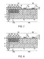
- Gate electrode stacks 49 are formed on the gate insulating film 28 in the peripheral transistor region 300 b .
- Each of the gate electrode stacks 49 has a metal gate film 30 , an upper gate film 32 , a fourth conductor film 40 obtained by processing the fifth conductor film 39 , and a third conductor film 44 obtained by processing the sixth conductor film 43 .
- low concentration impurity diffusion regions 46 n , 46 p and high concentration impurity diffusion regions 48 n , 48 p are formed in the semiconductor substrate 10 at the widthwise opposite ends of the gate electrode stack 49 .
- an insulating film 55 , capacitors 54 in the memory cell region 300 a , contact plugs 50 in the peripheral transistor region 300 b , upper wirings 51 , 53 , via plugs 52 and the like are formed to complete a DRAM 300 .
- the height B from the semiconductor substrate 10 to the top face of the metal gate film 30 may sometimes become greater than the height A from the semiconductor substrate 10 to the top face of the first interlayer insulating film 26 , or the height b of the top face of the upper gate film 32 may sometimes become higher than the height A of the of the top face of the first interlayer insulating film 26 , as shown in FIG. 18 .
- the metal gate film 30 and the upper gate film 32 for controlling threshold voltage of the peripheral transistors will be partially or totally removed.
- the CMP or etching is difficult to control when forming the formation of the contact plugs 42 , the second conductor film 45 and the gate electrode stacks 49 .
- the uniformity of the DRAM 300 may possibly be reduced and the yield of the DRAM 300 may be degraded.
- the steps of manufacturing the DRAM 300 after the formation of the contact plugs 42 , the second conductor film 45 and the gate electrode stacks 49 are performed separately between the memory cell region 300 a and the peripheral transistor region 300 b in order to avoid the aforementioned problem, the manufacturing process will become complicated.
- a semiconductor device comprising a semiconductor substrate including a memory cell region and a peripheral transistor region.
- the memory cell region comprises an embedded gate transistor for memory cell, a first interlayer insulating film having a bit contact hole, a contact plug formed of a first conductor film embedded in the bit contact hole, and a second conductor film which is stacked on the first interlayer insulating film to constitute a bit line connected to the contact plug.
- the peripheral transistor region comprises a peripheral transistor having a gate insulating film including a high-k film and a gate electrode stack formed on the gate insulating film.
- the gate electrode stack is provided at least with a metal gate film formed on the gate insulating film, an upper gate film stacked on the metal gate film, and a third conductor film stacked on the upper gate film.
- the third conductor film is formed of the same material and having the same thickness as the second conductor film.
- a height from the semiconductor substrate to a top face of the upper gate film is equal to or lower than a height of a top face of the first interlayer insulating film.
- a semiconductor device comprising a semiconductor substrate in which a first region and a second region are defined, a diffusion layer arranged on the semiconductor substrate in the first region, a first interlayer insulating film arranged on the first region, a contact plug passing through the first interlayer insulating film and electrically connected to the diffusion layer, and a transistor arranged in the second region and comprising a gate insulating film including a high-k film, a first conductor layer arranged on the gate insulating film, and a second conductor layer arranged on the first conductor layer.
- a height of a top face of the second conductor layer is equal to or lower than a height of a top face of the first interlayer insulating film.
- a semiconductor device comprising a semiconductor substrate in which a first region and a second region are defined, a diffusion layer arranged on the semiconductor substrate in the first region, a first interlayer insulating film arranged on the first region, a contact plug passing through the first interlayer insulating film and electrically connected to the diffusion layer, and a transistor arranged in the second region and comprising a gate insulating film, a metal layer arranged on the gate insulating film, and a first conductor layer arranged on the metal layer.
- a height of a top face of the first conductor layer is substantially the same as a height of a top face of the first interlayer insulating film.
- the height from the semiconductor substrate to the top face of the upper gate film is equal to or lower than the height from the semiconductor substrate to the top face of the first interlayer insulating film. Therefore, the first interlayer insulating film or the upper gate film functions as a CMP stopper or as an index for determining etching endpoint in the steps of forming the contact plugs, the second conductor film and the gate electrode stack. This makes it possible to prevent damage to or loss of the metal gate film and the upper gate film.
- the uniformity of the semiconductor device is improved. This facilitates gate etching and improves the yield of the semiconductor device.
- the semiconductor device manufacturing steps after the formation of the contact plugs, the second conductor film and the gate electrode stack in the memory cell region and the peripheral transistor region can be performed collectively.
- FIG. 1 is a cross-sectional view showing a configuration of a semiconductor device according to a first embodiment of the invention
- FIG. 2 is a cross-sectional view showing one manufacturing step of the semiconductor device according to the first embodiment of the invention
- FIG. 3 is a cross-sectional view showing a manufacturing step following the step of FIG. 2 ;
- FIG. 4 is a cross-sectional view showing a manufacturing step following the step of FIG. 3 ;
- FIG. 5 is a cross-sectional view showing a manufacturing step following the step of FIG. 4 ;
- FIG. 6 is a cross-sectional view showing a manufacturing step following the step of FIG. 5 ;
- FIG. 7 is a cross-sectional view showing a manufacturing step following the step of FIG. 6 ;
- FIG. 8 is a cross-sectional view showing a manufacturing step following the step of FIG. 7 ;
- FIG. 9 is a cross-sectional view showing a manufacturing step following the step of FIG. 8 ;
- FIG. 10 is a cross-sectional view showing a manufacturing step of the semiconductor device following the step of FIG. 9 ;
- FIG. 11 is a cross-sectional view showing a manufacturing step following the step of FIG. 10 ;
- FIG. 12 is a cross-sectional view showing a manufacturing step following the step of FIG. 11 ;
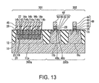
- FIG. 13 is a cross-sectional view showing a manufacturing step following the step of FIG. 12 ;
- FIG. 14 is a cross-sectional view showing a configuration of a semiconductor device according to a second embodiment of the invention.
- FIG. 15 is a cross-sectional view showing one manufacturing step of the semiconductor device according to the second embodiment of the invention.
- FIG. 16 is a cross-sectional view showing a manufacturing step following the step of FIG. 15 ;
- FIG. 17 is a cross-sectional view showing a manufacturing step following the step of FIG. 16 ;
- FIG. 18 is a cross-sectional view showing a configuration of a known semiconductor device
- FIG. 19 is a cross-sectional view showing one manufacturing step of the semiconductor device shown in FIG. 18 ;
- FIG. 20 is a cross-sectional view showing a manufacturing step following the step of FIG. 19 ;
- FIG. 21 is a cross-sectional view showing a manufacturing step following the step of FIG. 20 ;
- FIG. 22 is a cross-sectional view showing a manufacturing step following the step of FIG. 21 ;
- FIG. 23 is a cross-sectional view showing a manufacturing step following the step of FIG. 22 ;
- FIG. 24 is a cross-sectional view showing a manufacturing step following the step of FIG. 23 ;
- FIG. 25 is a cross-sectional view showing a manufacturing step following the step of FIG. 24 ;
- FIG. 26 is a cross-sectional view showing a manufacturing step following the step of FIG. 25 ;
- FIG. 27 is a cross-sectional view showing a manufacturing step following the step of FIG. 26 ;
- FIG. 28 is a cross-sectional view showing a manufacturing step following the step of FIG. 27 ;
- FIG. 29 is a cross-sectional view showing a manufacturing step following the step of FIG. 28 .
- FIGS. 1 to 17 A semiconductor device and a manufacturing method thereof according to the invention will be described with reference to FIGS. 1 to 17 .
- the same members or components are indicated by the same reference numerals and overlapping description will be omitted.
- the drawings used in the description are only schematic and ratios of length, width, and thickness of the components are not always the same as actual ones.
- a DRAM (semiconductor device) 401 according to a first embodiment of the invention and a manufacturing method thereof will be described with reference to FIGS. 1 to 13 .
- the DRAM 401 is composed of a memory cell region 300 a and a peripheral transistor region 300 b.
- the memory cell region (first region) 300 a and the peripheral transistor region (second region) 300 b are divided into a plurality of active regions 11 a , 11 b , and 11 c by STIs 12 formed in a semiconductor substrate 10 .
- FIG. 1 shows a configuration in which the active regions 11 a , 11 b , and 11 c are arranged adjacent to each other, the invention is not limited to this arrangement.
- a p-type silicon substrate is used for the semiconductor substrate 10 .
- a silicon oxide film is used for the STIs 12 .
- Memory cells of the DRAM 401 are provided in the active region 11 a .
- An n-channel and p-channel peripheral transistors are provided, respectively, in the active regions 11 b and 11 c.
- a configuration of memory cells formed in the active region 11 a is described.
- the memory cells of the DRAM 401 are of a 6F2 cell arrangement (F denotes a minimum processing dimension of the semiconductor device).
- Each of the memory cells of the DRAM 401 has an embedded gate transistor, a first interlayer insulating film 26 , a contact plug 42 , a second conductor film (fourth conductor layer) 45 , and a capacitor 54 .
- the embedded gate transistor for the memory cell has a gate insulating film 18 , a gate electrode 20 , an insulating film 23 , and impurity diffusion regions 14 a , 14 b.
- the gate insulating film 18 is provided on inner walls of each trench for gate electrode formed in the semiconductor substrate 10 in the active region 11 a .
- the gate insulating film 18 is formed of a silicon oxide film, for example.
- the gate electrode 20 is provided in a lower part of the trench surrounded by the gate insulating film 18 .
- the gate electrode 20 is formed of a metal having a high melting point such as tungsten.
- the insulating film 23 is provided to fill the trench surrounded by the gate insulating film 18 in the upper part of the gate electrode 20 .
- the insulating film 23 is formed, for example, of a silicon nitride film or a silicon oxide film.
- the impurity diffusion regions 14 a , 14 b are provided in an upper part of the semiconductor substrate 10 , between the adjacent gate electrodes 20 and between the gate electrode 20 and the STI 12 .
- the impurity diffusion regions 14 a , 14 b have an impurity dopant of a different conductivity type (n-type in the first embodiment) from that of the semiconductor substrate 10 , and are formed by implanting an n-type impurity dopant into the semiconductor substrate 10 , or by embedding an impurity semiconductor containing an n-type impurity dopant.
- Each of the impurity diffusion regions 14 a is connected to a second conductor film 45 constituting a bit line, via the contact plug 42 to be described later, and functions as a source region of the embedded gate transistor.
- Each of the impurity diffusion regions 14 b is connected to a capacitor 54 to be described later, and functions as a drain region of the embedded gate transistor.
- the first interlayer insulating film 26 is provided on memory cells formed by the embedded gate transistors and has bit contact holes 27 . The bottom of each bit contact hole 27 is in contact with the impurity diffusion region 14 a .
- the first interlayer insulating film 26 is formed, for example, of a silicon oxide film.
- the height A from the semiconductor substrate 10 to the top face of the first interlayer insulating film 26 is greater than the height B from the semiconductor substrate 10 to the top face of a metal gate film 30 to be described later.
- the height A of the top face of the first interlayer insulating film 26 is equal to or higher than the height b of the top face of the upper gate film 32 .
- Each of the contact plugs 42 is formed by embedding a first conductor film to be described later in the bit contact hole 27 .
- the first conductor film is formed, for example, of a metal film such as tungsten, or a doped polysilicon film.
- the second conductor film 45 is stacked on the first interlayer insulating film 26 .
- the second conductor film 45 is connected to the contact plugs 42 and constitutes bit lines of the memory cells.
- the capacitors 54 connected to the impurity diffusion regions 14 b are provided above the second conductor film 45 .
- the capacitors 54 may assume any structure generally used for a DRAM, such as cylinder type or crown type.
- Contact plugs may be provided between the capacitors 54 and the impurity diffusion regions 14 b.
- the active region 11 b has an n-channel peripheral transistor, contact plugs 50 , via plugs 52 , and upper wirings 51 , 53 .
- the n-channel peripheral transistor has a gate insulating film 28 , a gate electrode stack 49 , a low concentration impurity diffusion region 46 n , and a high concentration impurity diffusion region 48 n.
- the gate insulating film 28 is provided on the semiconductor substrate 10 in the active region 11 b via the insulating film 16 .
- the gate insulating film 28 includes a high-k film made of a high dielectric material such as hafnium.
- the gate electrode stack 49 has a metal gate film (first conductor layer) 30 , an upper gate film (second conductor layer) 32 , a fourth conductor film (third conductor layer) 40 , and a third conductor film (fifth conductor layer) 44 .
- the metal gate film 30 is provided on the gate insulating film 28 .
- the metal gate film 30 is formed of a metal film such as nickel film, which has good controllability on threshold voltage of the peripheral transistor when combined with the high-k film.
- the thickness of the metal gate film 30 is determined in accordance with the threshold voltage of the peripheral transistor.
- the height B from the semiconductor substrate 10 to the top face of the metal gate film 30 is smaller than the height A from the semiconductor substrate 10 to the top face of the first interlayer insulating film 26 .
- the upper gate film 32 is provided on the metal gate film 30 .
- the upper gate film 32 is formed, for example, of a doped polysilicon film.
- the thickness of the upper gate film 32 is determined in consideration of a threshold voltage of the peripheral transistor and the thickness of the metal gate film 30 .
- the height b of the top face of the upper gate film 32 is equal to or lower than the height A of the top face of the first interlayer insulating film 26 .
- the fourth conductor film 40 is provided between the upper gate film 32 and a third conductor film 44 to be described later.
- the fourth conductor film 40 is formed of the same material as that of the first conductor film constituting the contact plugs 42 .
- the height position of the top face of the fourth conductor film 40 is the same as the height position of the top face of the contact plug 42 .
- the third conductor film 44 is provided above the upper gate film 32 , that is, on the fourth conductor film 40 .
- the third conductor film 44 is formed of the same material as that of the second conductor film 45 , and has the same thickness as that of the second conductor film 45 . Therefore, the top face of the second conductor film 45 is flush with the top face of the third conductor film 44 .
- the threshold voltage of the peripheral transistor is determined based on the material and the total thickness of the gate electrode stack 49 .
- the thicknesses of the fourth conductor film 40 and the third conductor film 44 are determined respectively in consideration of a threshold voltage of the peripheral transistor.
- the low concentration impurity diffusion regions 46 n are provided in the semiconductor substrate 10 on the widthwise opposite sides of the gate electrode stack 49 formed in the active region 11 b .
- the low concentration impurity diffusion regions 46 n have an n-type impurity dopant and are formed by the same processes as the impurity diffusion regions 14 a and 14 b.
- the high concentration impurity diffusion regions 48 n are provided in the semiconductor substrate 10 , adjacent to the low concentration impurity diffusion regions 46 n on the sides closer to the STIs 12 .
- the high concentration impurity diffusion regions 48 n have a higher concentration of n-type impurity dopant than the low concentration impurity diffusion region 46 n , and are formed by the same processes as the impurity diffusion regions 14 a and 14 b.
- the low concentration impurity diffusion regions 46 n and the high concentration impurity diffusion regions 48 n function as source and drain regions of the n-channel peripheral transistor.
- Contact plugs 50 connected to the high concentration impurity diffusion regions 48 n are provided on the sides of the gate electrode stack 49 .
- the upper wiring 51 is provided in contact with the top face of each contact plug 50 .
- a via plug 52 is provided in contact with the upper wiring 51 .
- An upper wiring 53 is further provided on the via plug 52 .
- the contact plug 50 and the via plug 52 are formed of a metal film such as a tungsten film.
- a multilayer wiring may be formed on the upper wiring 53 .
- the active region 11 c has a p-channel peripheral transistor, a contact plug 50 , a via plug 52 , and upper wirings 51 and 53 .
- the p-channel peripheral transistor has a gate insulating film 28 , a gate electrode stack 49 , low concentration impurity diffusion regions 46 p , and high concentration impurity diffusion regions 48 p .
- the arrangement of the gate insulating film 28 and the gate electrode stack 49 of the p-channel peripheral transistor is the same as that of the gate insulating film 28 and the gate electrode stack 49 of the n-channel peripheral transistor, and hence description thereof will be omitted.
- the low concentration impurity diffusion regions 46 p are provided in the semiconductor substrate 10 on the widthwise opposite sides of the gate electrode stack 49 formed in the active region 11 c .
- the low concentration impurity diffusion regions 46 p have a p-type impurity dopant and are formed by the same processes as the impurity diffusion regions 14 a and 14 b.
- the high concentration impurity diffusion regions 48 p are provided in the semiconductor substrate 10 , adjacent to the low concentration impurity diffusion regions 46 p on the sides closer to the STIs 12 .
- the high concentration impurity diffusion regions 48 p have a higher concentration of p-type impurity dopant than the low concentration impurity diffusion regions 46 p , and are formed by the same processes as the impurity diffusion regions 14 a and 14 b.
- the low concentration impurity diffusion regions 46 p and the high concentration impurity diffusion regions 48 p function as source and drain regions of the p-channel peripheral transistor.
- the portion of the semiconductor substrate 10 in the active region 11 c may contain an impurity dopant of a different conductivity type (n-type impurity dopant) from that of the semiconductor substrate 10 , and may be provided with a well including the low concentration impurity diffusion region 46 n and the high concentration impurity diffusion region 48 n.
- impurity dopant of a different conductivity type n-type impurity dopant
- the arrangement of the contact plug 50 , the via plug 52 , and the upper wirings 51 , 53 of the p-channel peripheral transistor is the same as that of the contact plug 50 , the via plug 52 , and the upper wirings 51 , 53 of the n-channel peripheral transistor, and hence description thereof will be omitted.
- An insulating film 55 is provided to cover all the components in the memory cell region 300 a and the peripheral transistor region 300 b on the insulating film 16 .
- the insulating film 55 is formed, for example, of a silicon oxide film.
- a memory cell region 300 a and a peripheral transistor region 300 b are defined on the semiconductor substrate 10 . Further, an n-channel region 301 and a p-channel region 302 are defined on the semiconductor substrate 10 .
- a plurality of STIs 12 are formed to define active regions 11 a , 11 b , 11 c in the memory cell region 300 a and peripheral transistor region 300 b .
- Each of the STIs 12 can be formed, for example, by forming a trench in the semiconductor substrate 10 and then filling the trench with an insulating film such as a silicon oxide film by a CVD method.
- an insulating film 16 made of a silicon nitride film or the like is formed to cover the semiconductor substrate 10 and the STIs 12 .
- Each embedded gate transistor comprises a gate insulating film 18 , a gate electrode 20 , an insulating film 23 , and impurity diffusion regions 14 a and 14 b.
- a silicon oxide film 26 ′ is formed on the structure shown in FIG. 2 .
- the height A from the semiconductor substrate 10 to the top face of the silicon oxide film 26 ′ is smaller than the height from the semiconductor substrate 10 to a metal gate film to be formed later in the peripheral transistor region 300 b .
- the height A of the top face of the silicon oxide film 26 ′ is higher than the height of the top face of the upper gate film in the peripheral transistor region 300 b.
- the silicon oxide film 26 ′ is set to finally satisfy the aforementioned conditions in consideration of a threshold voltage of the peripheral transistor.
- a first interlayer insulating film 26 is formed on the embedded gate transistors for memory cells in the memory cell region 300 a.
- a high-k film 28 ′ is formed to cover the first interlayer insulating film 26 and the insulating film 16 in the peripheral transistor region 300 b .
- the high-k film 28 ′ may be formed of a material having a relative dielectric constant of 7.0 or more (e.g. Si 3 N 4 and Al 2 O 3 ).
- a metal gate film 30 and an upper gate film 32 are sequentially stacked by patterning on the active region 11 b in the peripheral transistor region 300 b .
- the metal gate film 30 may be formed of a metal film (e.g. nickel film) that is selected in accordance with the high-k film 28 ′.
- the upper gate film 32 may be formed of a doped polysilicon film.
- the thicknesses of the metal gate film 30 and the upper gate film 32 are determined respectively in consideration of a threshold voltage of the peripheral transistor.
- the height B from the semiconductor substrate 10 to the metal gate film 30 should be smaller than the height A from the semiconductor substrate 10 to the top face of the first interlayer insulating film 26 .
- the height b of the top face of the upper gate film 32 is equal to or lower than the height A of the top face of the first interlayer insulating film 26 .
- a metal gate film 30 and an upper gate film 32 are sequentially stacked by patterning on the active region 11 c in the peripheral transistor region 300 b .
- the metal gate film 30 and the upper gate film 32 in the active region 11 c may be formed of the same material as that of the metal gate film 30 and the upper gate film 32 in the active region 11 b .
- the respective thicknesses of the metal gate film 30 and the upper gate film 32 in the active region 11 c are the same as those of the metal gate film 30 and the upper gate film 32 in the active region 11 b .
- the metal gate films 30 and the upper gate films 32 in the active regions 11 b and 11 c may be formed collectively.
- the high-k film 28 ′ is removed except the portions thereof covered by the metal gate film 30 in the peripheral transistor region 300 b .
- gate insulating films 28 including a high-k film is formed on the active regions 11 b and 11 c in the peripheral transistor region 300 b.
- bit contact holes 27 are formed in the first interlayer insulating film 26 to be in contact with the respective impurity diffusion regions 14 a .
- the bit contact holes 27 can be formed by lithography and etching, for example.
- a fifth conductor film 39 is formed to cover the first interlayer insulating film 26 while filling the bit contact holes 27 , and to cover the upper gate film 32 .
- the fifth conductor film 39 is formed of a material used for contact plugs or gate electrodes of peripheral transistors, for example, a doped polysilicon film.
- the fifth conductor film 39 is removed downward from the top face thereof, by CMP or etching.
- the height A of the first interlayer insulating film 26 is equal to or higher than the height b of the top face of the upper gate film 32 . Therefore, when the fifth conductor film 39 is removed downward from the top face thereof, the top face of the first interlayer insulating film 26 is exposed from the top face of the fifth conductor film 39 first ( FIG. 11 ), or the top face of the first interlayer insulating film 26 and the top face of the upper gate film 32 are exposed simultaneously. The CMP or etching of the fifth conductor film 39 is stopped at this point. In this manner, the fifth conductor film 39 is flattened until the top face of the first interlayer insulating film 26 and/or the top face of the upper gate film 32 is exposed.
- contact plugs 42 which are formed of a first conductor film of the same material as that of the fifth conductor film 39 and embedded in the bit contact holes 27 in the first interlayer insulating film 26 .
- the fifth conductor film 39 can be left unremoved on the upper gate film 32 in the peripheral transistor region 300 b.
- the height position A of the top face of the first interlayer insulating film 26 , the height position of the top faces of the contact plugs 42 , and the height position of the top face of the fifth conductor film 39 or the upper gate film 32 in the peripheral transistor region 300 b can be all aligned to the same height.
- a sixth conductor film 43 is stacked on the first interlayer insulating film 26 and the upper gate film 32 .
- the sixth conductor film 43 is formed of a tungsten film or a material that is used for forming bit lines.
- the thickness of the sixth conductor film 43 is determined in consideration of the thickness of bit lines of the embedded gate transistors.
- the fifth conductor film 39 and the sixth conductor film 43 are removed by patterning, except the portions thereof locating on the first interlayer insulating film 26 and the upper gate film 32 .
- the height position A of the top face of the first interlayer insulating film 26 , the height position of the top faces of the contact plugs 42 , and the height position of the top face of the fifth conductor film 39 or the upper gate film 32 in the peripheral transistor region 300 b are aligned to the same height, and the top face of the sixth conductor film 43 is flattened, patterning of the fifth conductor film 39 and the sixth conductor film 43 can be performed easily with high precision. In addition, the patterning of the fifth conductor film 39 and the sixth conductor film 43 in the memory cell region 300 a and the peripheral transistor region 300 b can be performed collectively.
- a second conductor film 45 constituting a bit line connected to the contact plugs 42 is formed in the memory cell region 300 a .
- a gate electrode stack 49 is formed on the gate insulating film 28 in the peripheral transistor region 300 b .
- the gate electrode stack 49 has a metal gate film 30 , an upper gate film 32 , a fourth conductor film 40 formed by patterning the fifth conductor film 39 , and a third conductor film 44 having the same thickness as the second conductor film 45 and formed by patterning the sixth conductor film 43 .
- the total thickness of the gate electrode stack 49 controls the threshold voltage of the peripheral transistor.
- the respective thicknesses of the metal gate film 30 , the upper gate film 32 , the fourth conductor film 40 , and the third conductor film 44 are determined in consideration of the characteristics of the respective material and the threshold voltage of the peripheral transistor.
- the height A from the semiconductor substrate 10 to the top face of the first interlayer insulating film 26 is determined according to the total thickness of the gate insulating film 28 , the metal gate film 30 , the upper gate film 32 , and the fourth conductor film 40 .
- the height from the top face of the first interlayer insulating film 26 to the top face of the second conductor film 45 is determined according to the thickness of the third conductor film 44 that is determined in consideration of the thickness of the bit lines of the memory cells.
- low concentration impurity diffusion regions 46 n containing an n-type impurity dopant are formed in the semiconductor substrate 10 on the widthwise opposite sides of the gate electrode stack 49 in the active region 11 b .
- high concentration impurity diffusion regions 48 n containing an n-type impurity dopant are formed in the semiconductor substrate 10 adjacent to the low concentration impurity diffusion regions 46 n on the sides closer to the STIs 12 by means of the same process but increasing the concentration of the n-type impurity dopant.
- the n-type impurity dopant may be changed to a p-type impurity dopant and the same process as the formation of the low concentration impurity diffusion region 46 n and the high concentration impurity diffusion region 48 n may be performed in the active region 11 c , so that low concentration impurity diffusion regions 46 p and high concentration impurity diffusion regions 48 p containing the p-type impurity dopant are formed in the semiconductor substrate 10 on the widthwise opposite sides of the gate electrode stack 49 in the active region 11 c.
- a well having an n-type impurity dopant and including the low concentration impurity diffusion regions 46 p and the high concentration impurity diffusion regions 48 p may be formed in the active region 11 c.
- capacitors 54 in the memory cell region 300 a , contact plugs 50 , via plugs 52 , and upper wirings 51 , 53 in the peripheral transistor region 300 b , and an insulating film 55 are formed by a known method.
- a DRAM 401 is thus completed.
- the height B from the semiconductor substrate 10 to the top face of the metal gate film 30 is smaller than the height A from the semiconductor substrate 10 to the top face of the first interlayer insulating film 26
- the height b of the top face of the upper gate film 32 is equal to or lower than the height A of the top face of the first interlayer insulating film 26 .
- the first interlayer insulating film 26 or the upper gate film 32 functions as a CMP stopper, or an index for determining etching endpoint.
- the fifth conductor film 39 when the fifth conductor film 39 is processed, the fifth conductor film 39 can be flattened until the top face of the first interlayer insulating film 26 or the top face of the upper gate film 32 is exposed, so that the height of the top face of the upper gate film 32 is made equal to or lower than the height of the top face of the fifth conductor film 39 after completion of the processing. Therefore, damage to or loss of the metal gate film 30 and the upper gate film 32 can be prevented reliably.
- the uniformity of the DRAM 401 can be improved since the control of the CMP or etching is made easy during formation of the contact plugs 42 , the second conductor film 45 , and the gate electrode stack 49 . This facilitates the gate etching processing, which improves the yield of semiconductor device.
- the top face of the first interlayer insulating film 26 , the top faces of the contact plugs 42 , and the top face b of the fourth conductor film 40 or the upper gate film 32 can be aligned at the same position. Therefore, the manufacturing steps of the semiconductor device after the formation of the contact plugs 42 , the second conductor film 45 and the gate electrode stack 49 in the memory cell region 300 a and the peripheral transistor region 300 b can be performed collectively and easily.
- a DRAM (semiconductor device) 402 according to a second embodiment of the invention and a manufacturing method thereof will be described with reference to FIGS. 14 and 15 .
- FIG. 14 a configuration of the DRAM 402 will be described.
- like components of the DRAM 402 to those of the DRAM 401 shown in FIG. 1 will be indicated by the same reference numerals and description thereof will be omitted.
- the gate electrode stack 49 of the peripheral transistor does not necessarily require to include a polysilicon film or doped polysilicon film.
- the DRAM 402 has, as shown in FIG. 14 , a configuration in which the metal gate film 30 and the upper gate film 32 formed of a polysilicon film or doped polysilicon film, formed in the p-channel region 302 in the peripheral transistor region 300 b of the DRAM 401 are replaced with another metal gate film 34 .
- This another metal gate film 34 has the same thickness as the total thickness of the metal gate film 30 and the upper gate film 32 formed in the n-channel region 301 in the peripheral transistor region 300 b .
- the thickness of the metal gate film 34 is determined in consideration of a threshold voltage of the p-channel peripheral transistor.
- the another metal gate film 34 is formed of a metal film such as a nickel film.
- the configuration of the DRAM 402 according to the second embodiment is not limited to the configuration shown in FIG. 14 in which the another metal gate film 34 is used only in the p-channel peripheral transistor.
- the DRAM 402 according to the second embodiment may have a configuration in which only the metal gate film 30 and upper gate film 32 formed in the n-channel peripheral transistor are replaced with another metal gate film 34 , or the metal gate film 30 and upper gate film 32 formed in every peripheral transistor are replaced with a metal gate film 34 .
- a manufacturing method of the DRAM 402 will be described with reference to FIG. 15 .
- description of the manufacturing method of the DRAM 402 description of the same steps as those in the manufacturing method of the DRAM 401 will be omitted.
- the same steps as those in the manufacturing method of the DRAM 401 shown in FIGS. 1 to 6 are firstly performed, whereby a structure as shown in FIG. 6 is obtained.
- a metal gate film 34 having the same thickness as the total thickness of the metal gate film 30 and the upper gate film 32 formed in the active region 11 b is formed on a high-k film 28 ′ in the active region 11 c in the peripheral transistor region 300 b .
- the height of the top face of the upper gate film 32 in the active region 11 b is the same as the height of the top face of the metal gate film 34 in the active region 11 c.
- the metal gate film 34 can be formed of a metal film such as a nickel film.
- the metal gate film 34 can be formed, for example, by lithography and etching.
- the top face of the first interlayer insulating film 26 or the top face of the first interlayer insulating film 26 as well as the top face of the upper gate film 32 and the top face of the metal gate film 34 are exposed from the top face of the fifth conductor film 39 when the fifth conductor film 39 is removed downward from the top face thereof by CMP or etching. At this point, the CMP or etching of the fifth conductor film 39 is stopped.
- a metal gate film 34 is formed between the gate insulating film 28 and the third conductor film 44 in the active region 11 c in the peripheral transistor region 300 b , such that the height of the top face of the metal gate film 34 is the same as the height of the top face of the first interlayer insulating film 26 and the upper gate film 32 in the active region 11 b.
- the height B from the semiconductor substrate 10 to the top face of the metal gate film 30 can be made smaller than the height A from the semiconductor substrate 10 to the top face of the first interlayer insulating film 26
- the height b of the top face of the upper gate film 32 and the metal gate film 34 can be made equal to or lower than the height A of the top face of the first interlayer insulating film 26 .
- the first interlayer insulating film 26 or the upper gate film 32 or the metal gate film 34 functions as a CMP stopper or an index for determining the etching endpoint.
- the height of the upper gate film 32 and the height of the top face of the metal gate film 34 becomes equal to or lower than the height of the top face of the fifth conductor film 39 after completion of the processing. Therefore, the damage to or loss of the metal gate film 30 , the upper gate film 32 , and the metal gate film 34 can be prevented reliably.
- DRAM semiconductor device 403 (not shown in the drawings) according to a third embodiment of the invention and a manufacturing method thereof will be described with reference to FIGS. 16 and 17 .
- the DRAM 403 has a configuration in which the upper gate film 32 in the peripheral transistor region 300 b of the DRAM 401 is replaced with a hard mask film 62 , a seventh conductor film 60 is arranged between the metal gate film 30 and the hard mask film 62 , and the third conductor film 44 is removed.
- the seventh conductor film 60 is formed of a doped silicon film.
- the configuration of the DRAM 403 according to the third embodiment is the same as that of the DRAM 401 according to the first embodiment except for the layered structure of the seventh conductor film 60 and the hard mask film 62 in the peripheral transistor region 300 b . Therefore, in the description of the manufacturing method of the DRAM 403 , description of the same steps as those of the manufacturing method of the DRAM 401 will be omitted.
- the same steps as those of the manufacturing method of the DRAM 401 shown in FIGS. 1 to 5 are firstly performed, whereby a structure as shown in FIG. 5 is obtained.
- a metal gate film 30 , a seventh conductor film 60 , and a hard mask film 62 as an upper gate film are sequentially stacked by patterning on the high-k film 28 ′ in the active regions 11 b and 11 c in the peripheral transistor region 300 b .
- the seventh conductor film 60 may be formed of a doped polysilicon film.
- the hard mask film 62 may be formed of a silicon nitride film, for example.
- the thickness of the seventh conductor film 60 is determined in consideration of a threshold voltage of the peripheral transistor.
- the height of the top face of the hard mask film 62 is made equal to the height of the top face of the first interlayer insulating film 26 .
- the sixth conductor film 43 on the hard mask film 62 is also removed.
- a gate electrode stack 49 composed of a metal gate film 30 and a seventh conductor film 60 is formed on the gate insulating film 28 in the peripheral transistor region 300 b.
- the hard mask film 62 the top face of which is at a height equal to or lower than the height A of the top face of the first interlayer insulating film 26 is formed on the gate insulating film 28 in the active region 11 c in the peripheral transistor region 300 b . Additionally, the seventh conductor film 60 is formed between the metal gate film 30 and the hard mask film 62 .
- the first interlayer insulating film 26 or the hard mask film 62 functions as a CMP stopper.
- the height of the top face of the hard mask film 62 becomes equal to the height of the top face of the fifth conductor film 39 after completion of the processing, which makes it possible to reliably prevent the damage to or loss of the metal gate film 30 , the seventh conductor film 60 , and the hard mask film 62 .
- the top face of the first interlayer insulating film 26 , the top faces of the contact plugs 42 , and the top face of the hard mask film 62 can be aligned at the same position at completion of formation of the contact plugs 42 . Therefore, the manufacturing steps of the semiconductor device after the formation of the second conductor film 45 and the gate electrode stack 49 in the memory cell region 300 a and the peripheral transistor region 300 b can be carried out easily.
- the manufacturing method of a semiconductor device according to the third embodiment is able to provide the same advantageous effects as those of the manufacturing method of a semiconductor device according to the first embodiment even when the hard mask film 62 is left unremoved on the peripheral transistor region 300 b.
- the metal gate film 30 is referred to as the first conductor layer
- the upper gate film 32 is referred to as the second conductor layer
- the fourth conductor film 40 is referred to as the third conductor layer
- the second conductor film 45 is referred to as the fourth conductor layer
- the third conductor film 44 is referred to as the fifth conductor layer
- the metal gate film 30 may be referred to as a first metal layer.
- the upper gate film 32 and the fourth conductor film 40 can be combined together and referred to as a first conductor layer
- the second conductor film 45 can be referred to as a second conductor layer
- the third conductor film 44 can be referred as a third conductor layer.
- the invention has been described on the assumption that it is a DRAM as an example of semiconductor devices, the invention is applicable to semiconductor devices other than a DRAM as well.
- a manufacturing method of a semiconductor device comprising:
- a memory cell including an embedded gate transistor for memory cell in the memory cell region
- a metal gate film the top face of which has a height lower than a height of the top face of the first interlayer insulating film, while forming an upper gate film the top face of which has a height equal to or lower than a height of the top face of the first interlayer insulating film;
- a second conductor film constituting a bit line connected to the contact plug in the memory cell region by patterning the sixth conductor film, while forming, in the peripheral transistor region, a gate electrode stack including the metal gate film, the upper gate film, and a third conductor film formed by patterning the sixth conductor film.
- the upper gate film is formed of doped polysilicon and such that the position of the top face thereof is lower than the position of the top face of the first interlayer insulating film;
- the fifth conductor film is flattened until the top face of the first interlayer insulating film is exposed, and a fourth conductor film is formed on the upper gate film;
- the third conductor film is formed on the fourth conductor film.
- another metal gate film is formed on the gate insulating film, the another metal gate film having the same thickness as the total thickness of the metal gate film and the upper gate film;
- the fifth conductor film is stacked to cover the first interlayer insulating film so as to fill the bit contact hole, and to cover the other metal gate film.
Landscapes
- Semiconductor Memories (AREA)
- Chemical & Material Sciences (AREA)
- Crystallography & Structural Chemistry (AREA)
Abstract
Description
Claims (15)
Applications Claiming Priority (2)
| Application Number | Priority Date | Filing Date | Title |
|---|---|---|---|
| JP2012-058781 | 2012-03-15 | ||
| JP2012058781A JP2013191808A (en) | 2012-03-15 | 2012-03-15 | Semiconductor device and method for manufacturing semiconductor device |
Publications (2)
| Publication Number | Publication Date |
|---|---|
| US20130241009A1 US20130241009A1 (en) | 2013-09-19 |
| US8994122B2 true US8994122B2 (en) | 2015-03-31 |
Family
ID=49156880
Family Applications (1)
| Application Number | Title | Priority Date | Filing Date |
|---|---|---|---|
| US13/785,494 Active US8994122B2 (en) | 2012-03-15 | 2013-03-05 | Semiconductor device having a memory cell region and a peripheral transistor region |
Country Status (2)
| Country | Link |
|---|---|
| US (1) | US8994122B2 (en) |
| JP (1) | JP2013191808A (en) |
Cited By (1)
| Publication number | Priority date | Publication date | Assignee | Title |
|---|---|---|---|---|
| US20190096770A1 (en) * | 2017-09-25 | 2019-03-28 | Samsung Electronics Co., Ltd. | Semiconductor devices |
Families Citing this family (3)
| Publication number | Priority date | Publication date | Assignee | Title |
|---|---|---|---|---|
| US9502466B1 (en) | 2015-07-28 | 2016-11-22 | Taiwan Semiconductor Manufacturing Co., Ltd. | Dummy bottom electrode in interconnect to reduce CMP dishing |
| US10937785B2 (en) * | 2016-01-29 | 2021-03-02 | Taiwan Semiconductor Manufacturing Company Ltd. | Semiconductor device |
| US10741748B2 (en) | 2018-06-25 | 2020-08-11 | International Business Machines Corporation | Back end of line metallization structures |
Citations (9)
| Publication number | Priority date | Publication date | Assignee | Title |
|---|---|---|---|---|
| US20030011002A1 (en) * | 2001-07-11 | 2003-01-16 | Hitachi, Ltd. | Semiconductor integrated circuit device and production method thereof |
| JP2005142203A (en) | 2003-11-04 | 2005-06-02 | Elpida Memory Inc | Semiconductor device and manufacturing method thereof |
| US20080061357A1 (en) * | 2004-09-28 | 2008-03-13 | Makoto Sakuma | Semiconductor device with double barrier film |
| US20080191292A1 (en) * | 2007-02-12 | 2008-08-14 | International Business Machines Corporation | METAL GATES WITH LOW CHARGE TRAPPING AND ENHANCED DIELECTRIC RELIABILITY CHARACTERISTICS FOR HIGH-k GATE DIELECTRIC STACKS |
| US20090072289A1 (en) * | 2007-09-18 | 2009-03-19 | Dae-Ik Kim | Semiconductor device having reduced thickness, electronic product employing the same, and methods of fabricating the same |
| US20100155799A1 (en) * | 2008-12-22 | 2010-06-24 | Elpida Memory, Inc. | Semiconductor device and method for manufacturing the same |
| JP2011014689A (en) | 2009-07-01 | 2011-01-20 | Panasonic Corp | Semiconductor device and method of manufacturing the same |
| JP2011049282A (en) | 2009-08-26 | 2011-03-10 | Renesas Electronics Corp | Semiconductor device and method for manufacturing the same |
| US20110156119A1 (en) * | 2009-12-31 | 2011-06-30 | Samsung Electronics Co., Ltd. | Semiconductor memory devices and methods of forming the same |
Family Cites Families (7)
| Publication number | Priority date | Publication date | Assignee | Title |
|---|---|---|---|---|
| JP4627977B2 (en) * | 2003-10-14 | 2011-02-09 | ルネサスエレクトロニクス株式会社 | Semiconductor device |
| KR100868768B1 (en) * | 2007-02-28 | 2008-11-13 | 삼성전자주식회사 | CMOS semiconductor device and its manufacturing method |
| JP4647682B2 (en) * | 2008-11-12 | 2011-03-09 | パナソニック株式会社 | Semiconductor device and manufacturing method thereof |
| JP2010272596A (en) * | 2009-05-19 | 2010-12-02 | Renesas Electronics Corp | Manufacturing method of semiconductor device |
| JP2011003717A (en) * | 2009-06-18 | 2011-01-06 | Panasonic Corp | Semiconductor apparatus and method of manufacturing the same |
| JP2011129565A (en) * | 2009-12-15 | 2011-06-30 | Elpida Memory Inc | Semiconductor device and method of manufacturing the same |
| JP2012019035A (en) * | 2010-07-07 | 2012-01-26 | Elpida Memory Inc | Semiconductor device and method for manufacturing the same |
-
2012
- 2012-03-15 JP JP2012058781A patent/JP2013191808A/en not_active Ceased
-
2013
- 2013-03-05 US US13/785,494 patent/US8994122B2/en active Active
Patent Citations (9)
| Publication number | Priority date | Publication date | Assignee | Title |
|---|---|---|---|---|
| US20030011002A1 (en) * | 2001-07-11 | 2003-01-16 | Hitachi, Ltd. | Semiconductor integrated circuit device and production method thereof |
| JP2005142203A (en) | 2003-11-04 | 2005-06-02 | Elpida Memory Inc | Semiconductor device and manufacturing method thereof |
| US20080061357A1 (en) * | 2004-09-28 | 2008-03-13 | Makoto Sakuma | Semiconductor device with double barrier film |
| US20080191292A1 (en) * | 2007-02-12 | 2008-08-14 | International Business Machines Corporation | METAL GATES WITH LOW CHARGE TRAPPING AND ENHANCED DIELECTRIC RELIABILITY CHARACTERISTICS FOR HIGH-k GATE DIELECTRIC STACKS |
| US20090072289A1 (en) * | 2007-09-18 | 2009-03-19 | Dae-Ik Kim | Semiconductor device having reduced thickness, electronic product employing the same, and methods of fabricating the same |
| US20100155799A1 (en) * | 2008-12-22 | 2010-06-24 | Elpida Memory, Inc. | Semiconductor device and method for manufacturing the same |
| JP2011014689A (en) | 2009-07-01 | 2011-01-20 | Panasonic Corp | Semiconductor device and method of manufacturing the same |
| JP2011049282A (en) | 2009-08-26 | 2011-03-10 | Renesas Electronics Corp | Semiconductor device and method for manufacturing the same |
| US20110156119A1 (en) * | 2009-12-31 | 2011-06-30 | Samsung Electronics Co., Ltd. | Semiconductor memory devices and methods of forming the same |
Cited By (1)
| Publication number | Priority date | Publication date | Assignee | Title |
|---|---|---|---|---|
| US20190096770A1 (en) * | 2017-09-25 | 2019-03-28 | Samsung Electronics Co., Ltd. | Semiconductor devices |
Also Published As
| Publication number | Publication date |
|---|---|
| JP2013191808A (en) | 2013-09-26 |
| US20130241009A1 (en) | 2013-09-19 |
Similar Documents
| Publication | Publication Date | Title |
|---|---|---|
| US9865592B2 (en) | Method for FinFET integrated with capacitor | |
| US9472646B2 (en) | Dual work function buried gate type transistor and method for fabricating the same | |
| US9704988B2 (en) | Dual work function buried gate type transistor and method for fabricating the same | |
| US9601384B2 (en) | Method of forming a semiconductor device comprising first and second nitride layers | |
| US20150214313A1 (en) | Transistor having dual work function buried gate electrode and method for fabricating the same | |
| US10050036B2 (en) | Semiconductor structure having common gate | |
| US20140124863A1 (en) | Method and structure for forming a localized soi finfet | |
| US20120280291A1 (en) | Semiconductor device including gate openings | |
| US20130149854A1 (en) | Method of manufacturing semiconductor device and semiconductor device | |
| KR20190032683A (en) | A semiconductor memory device and a method for manufacturing the same | |
| US9263456B2 (en) | Semiconductor device and method for manufacturing the same | |
| US9793372B1 (en) | Integrated circuit including a dummy gate structure and method for the formation thereof | |
| KR20150137428A (en) | Dual work function bruied gate type transistor, method for manufacturing the same and electronic device having the same | |
| CN108010882B (en) | Method of manufacturing memory device | |
| TWI567939B (en) | Semiconductor device and method of manufacturing same | |
| TW201820450A (en) | Semiconductor device and method of fabricating the same | |
| US8994122B2 (en) | Semiconductor device having a memory cell region and a peripheral transistor region | |
| US6974987B2 (en) | Semiconductor device | |
| US20090224327A1 (en) | Plane mos and the method for making the same | |
| KR20150088813A (en) | Device and method for manufacturing same | |
| JP2013254860A (en) | Method for manufacturing semiconductor device | |
| JP2011129761A (en) | Method of manufacturing semiconductor device | |
| KR20240176681A (en) | Semiconductor memory device | |
| JP2014056862A (en) | Method for manufacturing semiconductor device | |
| JP2013093451A (en) | Semiconductor device manufacturing method |
Legal Events
| Date | Code | Title | Description |
|---|---|---|---|
| AS | Assignment |
Owner name: ELPIDA MEMORY, INC., JAPAN Free format text: ASSIGNMENT OF ASSIGNORS INTEREST;ASSIGNOR:FUJIMOTO, HIROYUKI;REEL/FRAME:029924/0774 Effective date: 20130222 |
|
| AS | Assignment |
Owner name: ELPIDA MEMORY INC., JAPAN Free format text: SECURITY AGREEMENT;ASSIGNOR:PS4 LUXCO S.A.R.L.;REEL/FRAME:032414/0261 Effective date: 20130726 |
|
| AS | Assignment |
Owner name: PS4 LUXCO S.A.R.L., LUXEMBOURG Free format text: ASSIGNMENT OF ASSIGNORS INTEREST;ASSIGNOR:ELPIDA MEMORY, INC.;REEL/FRAME:032901/0196 Effective date: 20130726 |
|
| FEPP | Fee payment procedure |
Free format text: PAYOR NUMBER ASSIGNED (ORIGINAL EVENT CODE: ASPN); ENTITY STATUS OF PATENT OWNER: LARGE ENTITY |
|
| STCF | Information on status: patent grant |
Free format text: PATENTED CASE |
|
| AS | Assignment |
Owner name: PS5 LUXCO S.A.R.L., LUXEMBOURG Free format text: ASSIGNMENT OF ASSIGNORS INTEREST;ASSIGNOR:PS4 LUXCO S.A.R.L.;REEL/FRAME:039818/0506 Effective date: 20130829 Owner name: LONGITUDE SEMICONDUCTOR S.A.R.L., LUXEMBOURG Free format text: CHANGE OF NAME;ASSIGNOR:PS5 LUXCO S.A.R.L.;REEL/FRAME:039793/0880 Effective date: 20131112 |
|
| AS | Assignment |
Owner name: LONGITUDE LICENSING LIMITED, IRELAND Free format text: ASSIGNMENT OF ASSIGNORS INTEREST;ASSIGNOR:LONGITUDE SEMICONDUCTOR S.A.R.L.;REEL/FRAME:046863/0001 Effective date: 20180731 |
|
| MAFP | Maintenance fee payment |
Free format text: PAYMENT OF MAINTENANCE FEE, 4TH YEAR, LARGE ENTITY (ORIGINAL EVENT CODE: M1551); ENTITY STATUS OF PATENT OWNER: LARGE ENTITY Year of fee payment: 4 |
|
| MAFP | Maintenance fee payment |
Free format text: PAYMENT OF MAINTENANCE FEE, 8TH YEAR, LARGE ENTITY (ORIGINAL EVENT CODE: M1552); ENTITY STATUS OF PATENT OWNER: LARGE ENTITY Year of fee payment: 8 |