US8970304B2 - Hybrid amplifier - Google Patents
Hybrid amplifier Download PDFInfo
- Publication number
- US8970304B2 US8970304B2 US13/740,013 US201313740013A US8970304B2 US 8970304 B2 US8970304 B2 US 8970304B2 US 201313740013 A US201313740013 A US 201313740013A US 8970304 B2 US8970304 B2 US 8970304B2
- Authority
- US
- United States
- Prior art keywords
- transistor
- transistors
- pair
- cascode circuit
- drain
- Prior art date
- Legal status (The legal status is an assumption and is not a legal conclusion. Google has not performed a legal analysis and makes no representation as to the accuracy of the status listed.)
- Active, expires
Links
- 238000000034 method Methods 0.000 claims abstract description 16
- 230000002708 enhancing effect Effects 0.000 abstract 1
- 230000006854 communication Effects 0.000 description 22
- 238000004891 communication Methods 0.000 description 22
- 101100337798 Drosophila melanogaster grnd gene Proteins 0.000 description 8
- 230000003287 optical effect Effects 0.000 description 4
- 238000005516 engineering process Methods 0.000 description 3
- 230000006870 function Effects 0.000 description 3
- 238000013461 design Methods 0.000 description 2
- 239000000835 fiber Substances 0.000 description 2
- 239000002245 particle Substances 0.000 description 2
- 230000003321 amplification Effects 0.000 description 1
- 230000007175 bidirectional communication Effects 0.000 description 1
- 230000005540 biological transmission Effects 0.000 description 1
- 239000003990 capacitor Substances 0.000 description 1
- 230000001413 cellular effect Effects 0.000 description 1
- 238000004590 computer program Methods 0.000 description 1
- 238000010586 diagram Methods 0.000 description 1
- 238000012986 modification Methods 0.000 description 1
- 230000004048 modification Effects 0.000 description 1
- 238000003199 nucleic acid amplification method Methods 0.000 description 1
- 230000003071 parasitic effect Effects 0.000 description 1
- 230000002093 peripheral effect Effects 0.000 description 1
- 238000012545 processing Methods 0.000 description 1
- 238000012546 transfer Methods 0.000 description 1
Images


Classifications
-
- H—ELECTRICITY
- H03—ELECTRONIC CIRCUITRY
- H03F—AMPLIFIERS
- H03F3/00—Amplifiers with only discharge tubes or only semiconductor devices as amplifying elements
- H03F3/45—Differential amplifiers
- H03F3/45071—Differential amplifiers with semiconductor devices only
- H03F3/45076—Differential amplifiers with semiconductor devices only characterised by the way of implementation of the active amplifying circuit in the differential amplifier
- H03F3/45376—Differential amplifiers with semiconductor devices only characterised by the way of implementation of the active amplifying circuit in the differential amplifier using junction FET transistors as the active amplifying circuit
-
- H—ELECTRICITY
- H03—ELECTRONIC CIRCUITRY
- H03F—AMPLIFIERS
- H03F1/00—Details of amplifiers with only discharge tubes, only semiconductor devices or only unspecified devices as amplifying elements
- H03F1/08—Modifications of amplifiers to reduce detrimental influences of internal impedances of amplifying elements
- H03F1/22—Modifications of amplifiers to reduce detrimental influences of internal impedances of amplifying elements by use of cascode coupling, i.e. earthed cathode or emitter stage followed by earthed grid or base stage respectively
- H03F1/223—Modifications of amplifiers to reduce detrimental influences of internal impedances of amplifying elements by use of cascode coupling, i.e. earthed cathode or emitter stage followed by earthed grid or base stage respectively with MOSFET's
-
- H—ELECTRICITY
- H03—ELECTRONIC CIRCUITRY
- H03F—AMPLIFIERS
- H03F3/00—Amplifiers with only discharge tubes or only semiconductor devices as amplifying elements
- H03F3/45—Differential amplifiers
- H03F3/45071—Differential amplifiers with semiconductor devices only
- H03F3/45076—Differential amplifiers with semiconductor devices only characterised by the way of implementation of the active amplifying circuit in the differential amplifier
- H03F3/45179—Differential amplifiers with semiconductor devices only characterised by the way of implementation of the active amplifying circuit in the differential amplifier using MOSFET transistors as the active amplifying circuit
- H03F3/45183—Long tailed pairs
- H03F3/45188—Non-folded cascode stages
-
- H—ELECTRICITY
- H03—ELECTRONIC CIRCUITRY
- H03F—AMPLIFIERS
- H03F2200/00—Indexing scheme relating to amplifiers
- H03F2200/61—Indexing scheme relating to amplifiers the cascode amplifier has more than one common gate stage
-
- H—ELECTRICITY
- H03—ELECTRONIC CIRCUITRY
- H03F—AMPLIFIERS
- H03F2203/00—Indexing scheme relating to amplifiers with only discharge tubes or only semiconductor devices as amplifying elements covered by H03F3/00
- H03F2203/45—Indexing scheme relating to differential amplifiers
- H03F2203/45056—One or both transistors of the cascode stage of a differential amplifier being composed of more than one transistor
-
- H—ELECTRICITY
- H03—ELECTRONIC CIRCUITRY
- H03F—AMPLIFIERS
- H03F2203/00—Indexing scheme relating to amplifiers with only discharge tubes or only semiconductor devices as amplifying elements covered by H03F3/00
- H03F2203/45—Indexing scheme relating to differential amplifiers
- H03F2203/45184—Indexing scheme relating to differential amplifiers the differential amplifier has one or more cascode current sources in the load
-
- H—ELECTRICITY
- H03—ELECTRONIC CIRCUITRY
- H03F—AMPLIFIERS
- H03F2203/00—Indexing scheme relating to amplifiers with only discharge tubes or only semiconductor devices as amplifying elements covered by H03F3/00
- H03F2203/45—Indexing scheme relating to differential amplifiers
- H03F2203/45301—Indexing scheme relating to differential amplifiers there are multiple cascaded folded or not folded common gate stages of a cascode dif amp
-
- H—ELECTRICITY
- H03—ELECTRONIC CIRCUITRY
- H03F—AMPLIFIERS
- H03F2203/00—Indexing scheme relating to amplifiers with only discharge tubes or only semiconductor devices as amplifying elements covered by H03F3/00
- H03F2203/45—Indexing scheme relating to differential amplifiers
- H03F2203/45311—Indexing scheme relating to differential amplifiers the common gate stage of a cascode dif amp being implemented by multiple transistors
-
- H—ELECTRICITY
- H03—ELECTRONIC CIRCUITRY
- H03F—AMPLIFIERS
- H03F2203/00—Indexing scheme relating to amplifiers with only discharge tubes or only semiconductor devices as amplifying elements covered by H03F3/00
- H03F2203/45—Indexing scheme relating to differential amplifiers
- H03F2203/45364—Indexing scheme relating to differential amplifiers the AAC comprising multiple transistors parallel coupled at their gates and sources only, e.g. in a cascode dif amp, only those forming the composite common source transistor
-
- H—ELECTRICITY
- H03—ELECTRONIC CIRCUITRY
- H03F—AMPLIFIERS
- H03F2203/00—Indexing scheme relating to amplifiers with only discharge tubes or only semiconductor devices as amplifying elements covered by H03F3/00
- H03F2203/45—Indexing scheme relating to differential amplifiers
- H03F2203/45371—Indexing scheme relating to differential amplifiers the AAC comprising parallel coupled multiple transistors at their source and gate and drain or at their base and emitter and collector, e.g. in a cascode dif amp, only those forming the composite common source transistor or the composite common emitter transistor respectively
-
- H—ELECTRICITY
- H03—ELECTRONIC CIRCUITRY
- H03F—AMPLIFIERS
- H03F2203/00—Indexing scheme relating to amplifiers with only discharge tubes or only semiconductor devices as amplifying elements covered by H03F3/00
- H03F2203/45—Indexing scheme relating to differential amplifiers
- H03F2203/45661—Indexing scheme relating to differential amplifiers the LC comprising one or more controlled floating gates
Definitions
- the present invention relates generally to a telescopic amplifier. More specifically, the present invention relates to methods and devices for increasing a gain of a telescopic amplifier.
- Amplifiers are commonly used in various electronic devices to provide signal amplification. Various types of amplifiers are available and include voltage amplifiers, current amplifiers, etc. A voltage amplifier receives and amplifier an input voltage signal and provides an output voltage signal. A current amplifier receives and amplifier an input current signal and provides an output current signal. Amplifiers typically have different designs and are used in different applications.
- a wireless communication device such as a cellular phone may include a transmitter and a receiver for bi-directional communication. The transmitter may utilize a driver amplifier (DA) and a power amplifier (PA), the receiver may utilize a low noise amplifier (LNA), and the transmitter and receiver may utilize variable an amplifiers (VGAs).
- DA driver amplifier
- PA power amplifier
- LNA low noise amplifier
- VGAs variable an amplifiers
- Telescopic amplifiers which may include simple architectures and high bandwidths, are a desirable choice for many applications.
- increasing a DC gain of a telescopic amplifier e.g., via gain boosting, using longer channel length for devices, triple cascoding, etc.
- FIG. 1 illustrates a wireless communication device, according to an exemplary embodiment of the present invention.
- FIG. 2 is a telescopic amplifier including an input device, and first cascode device, and a second cascode device.
- FIG. 3 illustrates an amplifier, according to an exemplary embodiment of the present invention.
- FIG. 4 is a plot illustrating a comparison of gains of two amplifiers relative to input frequency.
- FIG. 5 is another plot illustrating a comparison of gains of two amplifiers relative to output voltage.
- FIG. 6 illustrates another amplifier, in accordance with an exemplary embodiment of the present invention.
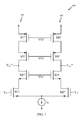
- FIG. 7 is another telescopic amplifier including an input device, a first cascode device, and a second cascode device.
- FIG. 8 illustrates yet another amplifier, in accordance with an exemplary embodiment of the present invention.
- FIG. 9 is a flowchart illustrating a method, according to an exemplary embodiment of the present invention.
- FIG. 10 is a flowchart illustrating another method, according to an exemplary embodiment of the present invention.
- the amplifier may include an input device including a differential pair of transistors.
- the amplifier may also include a cascode device including a first pair of transistors coupled to a first transistor of the differential pair and a second pair of transistors coupled to a second transistor of the differential pair.
- Each transistor of the cascode device may share a common gate bias voltage.
- FIG. 1 illustrates a wireless communication device 100 , according to an exemplary embodiment of the present invention.
- Wireless communication device 100 may be an access terminal, a mobile station, a user equipment (UE), etc.
- Wireless communication device 100 includes a processor 102 .
- Processor 102 may be a general purpose single or multi-chip microprocessor (e.g., an ARM), a special purpose microprocessor (e.g., a digital signal processor (DSP)), a microcontroller, a programmable gate array, etc.
- Processor 102 may be referred to as a central processing unit (CPU).
- CPU central processing unit
- Wireless communication device 100 also includes memory 104 .
- Memory 104 may be any electronic component capable of storing electronic information.
- Memory 104 may be embodied as random access memory (RAM), read-only memory (ROM), magnetic disk storage media, optical storage media, flash memory devices in RAM, on-board memory included with the processor, EPROM memory, EEPROM memory, registers and so forth, including combinations thereof.
- Data 106 a and instructions 108 a may be stored in memory 104 .
- Instructions 108 a may be executable by the processor 102 to implement the methods disclosed herein. Executing the instructions 108 a may involve the use of data 106 a that is stored in memory 104 .
- processor 102 executes instructions 108
- various portions of the instructions 108 b may be loaded onto processor 102
- various pieces of data 106 b may be loaded onto processor 102 .
- Wireless communication device 100 may also include a transmitter 110 and a receiver 112 to allow transmission and reception of signals to and from wireless communication device 100 via a first antenna 115 a and a second antenna 115 b .
- Transmitter 110 and receiver 112 may be collectively referred to as a transceiver 114 .
- Wireless communication device 100 may also include (not shown) multiple transmitters, additional antennas, multiple receivers and/or multiple transceivers.
- Wireless communication device 100 may include a digital signal processor (DSP) 116 .
- Wireless communication device 100 may also include a communications interface 118 .
- Communications interface 118 may allow a user to interact with wireless communication device 100 .
- the various components of wireless communication device 100 may be coupled together by one or more buses, which may include a power bus, a control signal bus, a status signal bus, a data bus, etc.
- buses may include a power bus, a control signal bus, a status signal bus, a data bus, etc.
- the various buses are illustrated in FIG. 1 as a bus system 120 .
- wireless communication device 100 may include one or more of amplifier 300 as described below with reference to FIG. 3 , one or more of amplifier 500 as described below with reference to FIG. 6 , one or more of amplifier 700 as described below with reference to FIG. 8 , or any combination thereof. It is further noted that wireless communication device 100 is an only an exemplary implementation of a wireless communication device and the invention may include other wireless communication devices configurations. Further, according to one exemplary embodiment of the present invention, one or more of the amplifiers described herein may implemented within one or more of an analog-to-digital converter (ADC), an electronic filter, and a power management circuit of a device (e.g., wireless communication device 100 ).
- ADC analog-to-digital converter
- FIG. 2 illustrates a telescopic amplifier 200 including a current source I b1 and a plurality of transistors M 1 -M 8 .
- amplifier 100 includes a differential input including transistors M 1 and M 2 .
- Transistor M 1 is configured to receive an input voltage V i1 at its gate and transistor M 2 is configured to receive an input voltage V i2 at its gate.
- Each of transistors M 1 and M 2 may be referred to as an input device.
- amplifier 200 includes transistors M 3 and M 4 , each of which may be referred to as a first cascode device or an upper cascode device.
- amplifier 200 includes transistors M 5 and M 6 , each of which may be referred to as a second cascode device or a lower cascode device.
- Amplifier 200 also transistors M 7 and M 8 , each of which may be referred to as an active load device.
- Transistors M 7 and M 8 which are respectively coupled to transistors M 5 and M 6 , are coupled to a ground voltage GRND.
- a bias voltage Vb 1 may be applied to the gates of transistors M 3 and M 4
- a bias voltage Vb 2 may be applied to the gates of transistors M 5 and M 6
- a bias voltage Vb 3 may be applied to the gates of transistors M 7 and M 8
- An output voltage V o1 may be coupled between a drain of transistor M 4 and a drain of transistor M 6
- an output voltage V o2 may be coupled between a drain of transistor M 3 and a drain of transistor M 5 .
- amplifier 100 includes a path 201 , which includes current source I b1 and transistors M 1 , M 3 , M 5 , and M 7 , for generating output voltage V o2
- amplifier 200 includes another path 203 , which includes current source I b1 and transistors M 2 , M 4 , M 6 , and M 8 , for generating output voltage V o1 .
- telescopic amplifiers such as telescopic amplifier 200
- increasing a DC gain of a telescopic amplifier e.g., via gain boosting, increasing channel lengths, or triple cascoding
- Gmx is the transconductance of the upper cascode device (e.g., transistor M 4 )
- rox the output impedance of the upper cascode device (e.g., transistor M 4 )
- roz is the output impedance
- a transconductance and/or an output impedance of one or more devices (e.g., transistors) of the amplifier may be increased.
- increasing a transconductance may require additional power and increasing an output impedance may require a size increase.
- FIG. 3 illustrates an amplifier 300 , according to an exemplary embodiment of the present invention.
- Amplifier 300 includes transistors M 7 -M 18 , current source I b1 , input voltages V i1 and V i2 , and output voltages V o1 ′ and V o2 ′. More specifically, amplifier 300 includes a differential input including transistors M 9 -M 12 . As illustrated, a gate of each of transistor M 9 and transistor M 10 is configured to receive input voltage V i1 , and a gate of each of transistor M 11 and transistor M 12 is configured to receive input voltage V i2 . Further, a source of each of transistors M 9 -M 12 is coupled to current source I b1 .
- a size of each of transistors M 9 -M 12 is a fraction of a size of each of transistors M 1 and M 2 (see FIG. 2 ).
- a size of each of transistors M 9 -M 12 is a one-half the size of each of transistors M 1 and M 2 .
- amplifier 300 includes first cascode circuit including transistors M 13 -M 16 and second cascode circuit including transistors M 17 and M 18 .
- transistors M 13 -M 16 may be referred to as a first cascode device or an upper cascode device and each of transistors M 17 and M 18 may be referred to as a second cascode device or a lower cascode device.
- Amplifier 300 also includes transistors M 7 and M 8 , each of which, as noted above, may be referred to as an active load device.
- a drain of transistor M 9 is coupled to a source of transistor M 13
- a drain of transistor M 10 is coupled to a source of transistor M 4 .
- a drain of transistor M 12 is coupled to a source of transistor M 16
- a drain of transistor M 11 is coupled to a source of transistor M 15 .
- a gate of each of transistors M 13 -M 16 is configured to receive a bias voltage Vb 1
- a gate of each of transistors M 17 and M 18 is configured to receive a bias voltage Vb 2
- a gate of each of transistors M 7 and M 8 is configured to receive a bias voltage Vb 3 .
- a drain of transistor M 13 is coupled to a drain of transistor M 17
- a drain of transistor M 14 is coupled to a source of transistor M 17
- a drain of transistor M 16 is coupled to a drain of transistor M 18
- a drain of transistor M 15 is coupled to a source of transistor M 18
- a source of transistor M 17 is coupled to a drain of transistor M 7 , which includes a source coupled to a ground voltage GRND.
- a source of transistor M 18 is coupled to a drain of transistor M 8 , which includes a source coupled to ground voltage GRND.
- Output voltage V o1 ′ is coupled between a drain of transistor M 16 and a drain of transistor M 18
- output voltage V o2 ′ is coupled between a drain of transistor M 13 and a drain of transistor M 17 .
- amplifier 300 includes a path 301 , which includes current source I b1 and transistors M 9 , M 13 , M 17 , and M 7 and a path 302 , which includes current source I b1 and transistors M 10 , M 14 , M 17 , and M 7 .
- amplifier 300 includes a path 303 , which includes current source I b1 and transistors M 11 , M 15 , M 18 , and M 8 , and a path 304 , which includes current source I b1 and transistors M 12 , M 16 , M 18 , and M 8 .
- Paths 301 and 302 are configured to generate output voltage V o2 ′ and paths 303 and 304 are configured to generate output voltage V o2 ′.
- a size of each of transistors M 13 -M 16 is a fraction of a size of each of transistors M 3 and M 4 (see FIG. 2 ), and a size of each of transistors M 17 and M 18 is a fraction of a size of each of transistors M 5 and M 6 (see FIG. 2 ).
- a size of each of transistors M 13 -M 16 is a one-half the size of each of transistors M 3 and M 4
- a size of each of transistors M 17 and M 18 is a one-half the size of each of transistors M 5 and M 6 .
- an amount of current in each path of amplifier 300 may reduced by a factor of two, an output impedance of each upper cascode device may be increased by a factor of two, an output impedance of each lower cascode device may be increased by a factor of two, an output impedance of each input device may be increased by a factor of two, a transconductance of each lower cascode device may reduced by a factor of two, and a transconductance of each upper cascode device may reduced by a factor of two.
- R′up which is the output impedance of the upper cascode combination (e.g., transistors M 12 and M 16
- R′down which is the output impedance of the lower cascode combination (e.g., transistor M 18 and M 8 )
- R′ up ( Gmx′/ 2)*(2 rox )*(2 roz );
- R′ down ( Gmy′/ 2)*(2 roy )* rozn;
- Gmx′ is the transconductance of the upper cascode devices (e.g., transistors M 15 and M 16 )
- rox is the output impedance of the upper cascode devices (e.g., transistors M 15 and M 16 )
- roz is the output impedance of the input devices (e.g., transistor M 11 and M 12 )
- Gmy′ is the transconductance of the lower cascode device (e.g., transistor M 18 )
- roy is the output impedance of the lower cascode device (e.g.
- FIG. 4 is a plot 400 illustrating amplifier gain relative to frequency. More specifically, waveform 402 illustrates a gain of a conventional amplifier (e.g., amplifier 100 ) and waveform 404 illustrates a gain of an amplifier (e.g., amplifier 200 ) according to an exemplary embodiment of the present invention. As depicted in plot 400 , the gain illustrated by waveform 404 is approximately 4 dB higher than the gain illustrated by waveform 402 .
- FIG. 5 is another plot 450 illustrating amplifier gain relative to an output swing. More specifically, waveform 452 illustrates a gain of a conventional amplifier (e.g., amplifier 200 ) and waveform 454 illustrates a gain of an amplifier (e.g., amplifier 300 ) according to an exemplary embodiment of the present invention. As depicted in plot 450 , the gain illustrated by waveform 454 is approximately 4 dB higher than the gain illustrated by waveform 452 .
- FIG. 6 is another amplifier 500 , in accordance with an exemplary embodiment of the present invention.
- Amplifier 500 includes transistors M 1 , M 2 , M 7 , M 8 , and M 13 -M 18 , current source I b1 , input voltages V i1 and V i2 , and output voltages V o1 ′′ and V o2 ′′.
- amplifier 500 includes a first cascode circuit including transistors M 13 -M 16 and a second cascode circuit including transistors M 17 and M 18 .
- Each of transistors M 13 -M 16 may be referred to as a first cascode device or an upper cascode device and each of transistors M 17 and M 18 may be referred to as a second cascode device or a lower cascode device.
- a gate of transistor M 1 is configured to receive input voltage V i1
- a gate of transistor M 2 is configured to receive input voltage V i2
- a source of each of transistors M 1 and M 2 is coupled to current source I b1
- a drain of transistor M 1 is coupled to a source of transistor M 13 and a source of transistor M 14
- a drain of transistor M 2 is coupled to a source of transistor M 15 and a source of transistor M 16 .
- a gate of each of transistors M 13 -M 16 is configured to receive a bias voltage Vb 1
- a gate of each of transistors M 17 and M 18 is configured to receive a bias voltage Vb 2
- a gate of each of transistors M 7 and M 8 is configured to receive a bias voltage Vb 3
- a drain of transistor M 13 is coupled to a drain of transistor M 17
- a drain of transistor M 14 is coupled to a source of transistor M 17
- a drain of transistor M 16 is coupled to a drain of transistor M 18
- a drain of transistor M 15 is coupled to a source of transistor M 18 .
- a source of transistor M 17 is coupled to a drain of transistor M 7 , which includes a source coupled to ground voltage GRND.
- a source of transistor M 18 is coupled to a drain of transistor M 8 , which includes a source coupled to ground voltage GRND.
- Output voltage V o1 ′′ is coupled between a drain of transistor M 16 and a drain of transistor M 18
- output voltage V o2 ′′ is coupled between a drain of transistor M 13 and a drain of transistor M 17 .
- amplifier 500 includes a path 501 , which includes current source I b1 and transistors M 1 , M 13 , M 17 , and M 7 and a path 502 , which includes current source I b1 and transistors M 1 , M 14 , M 17 , and M 7 .
- amplifier 500 includes a path 503 , which includes current source I b1 and transistors M 2 , M 15 , M 18 , and M 8 , and a path 504 , which includes current source I b1 and transistors M 2 , M 16 , M 18 , and M 8 .
- Paths 501 and 502 are configured to generate output voltage V o2 ′′ and paths 503 and 504 are configured to generate output voltage V o1 ′′.
- an amount of current in each path of amplifier 500 may reduced by a factor of two, an output impedance of each upper cascode device may be increased by a factor of two, an output impedance of each lower cascode device may be increased by a factor of two, a transconductance of each lower cascode device may reduced by a factor of two, and a transconductance of each upper cascode device may reduced by a factor of two. Therefore, in comparison amplifier 200 , the gain of amplifier 500 is increased (e.g., around 4 dB).
- amplifiers 200 , 300 , and 500 include PMOS input devices.
- the present invention is not so limited. Rather, as illustrated in FIGS. 7 and 8 , the present invention may include an NMOS input devices.
- FIG. 7 illustrates a telescopic amplifier 600 including current source I b1 and a plurality of transistors M 1 ′-M 8 ′. More specifically, amplifier 600 includes a differential input including transistors M 1 ′ and M 2 ′. Transistor M 1 ′ is configured to receive voltage V i1 at its gate and transistor M 2 ′ is configured to receive voltage V i2 at its gate. Each of transistors M 1 ′ and M 2 ′ may be referred to as an input device. In addition, amplifier 600 includes transistors M 3 ′ and M 4 ′, each of which may be referred to as a first cascode device or a lower cascode device.
- amplifier 600 includes transistors M 5 and M 6 , each of which may be referred to as a second cascode device or an upper cascode device.
- Amplifier 600 also includes transistors M 7 ′ and M 8 ′, each of which may be referred to as an active load device.
- Transistors M 7 ′ and M 8 ′ which are respectively coupled to transistors M 5 ′ and M 6 ′, are coupled to ground voltage GRND.
- Bias voltage Vb 1 may be applied to the gates of transistors M 3 ′ and M 4 ′
- bias voltage Vb 2 may be applied to the gates of transistors M 5 ′ and M 6 ′
- bias voltage Vb 3 may be applied to the gates of transistors M 7 ′ and M 8 ′.
- An output voltage V o1 ′′′ may be coupled between a drain of transistor M 4 ′ and a drain of transistor M 6 ′
- an output voltage V o2 ′′′ may be coupled between a drain of transistor M 3 ′ and a drain of transistor M 5 ′.
- amplifier 600 includes a path 601 , which includes current source I b1 and transistors M 1 ′, M 3 ′, M 5 ′, and M 7 ′, for generating output voltage V o2 ′′′.
- amplifier 600 includes another path 603 , which includes current source I b1 and transistors M 2 ′, M 4 ′, M 6 ′, and M 8 ′, for generating output voltage V o1 ′′′.
- FIG. 8 illustrates an amplifier 700 , according to an exemplary embodiment of the present invention.
- Amplifier 700 includes transistors M 7 ′-M 18 ′, current source I b1 , input voltages V i1 and V i2 , and output voltages V o1 ′′′′ and V o1 ′′′′. More specifically, amplifier 700 includes a differential input including transistors M 9 ′-M 12 ′. As illustrated, a gate of each of transistor M 9 ′ and transistor M 10 ′ is configured to receive input voltage V i1 , and a gate of each of transistor M 11 ′ and transistor M 12 ′ is configured to receive input voltage V i2 .
- a source of each of transistors M 9 ′-M 12 ′ is coupled to current source I b1 .
- a size of each of transistors M 9 ′-M 12 ′ is a fraction of a size of each of transistors M 1 ′ and M 2 ′ (see FIG. 7 ).
- a size of each of transistors M 9 ′-M 12 ′ is a one-half the size of each of transistors M 1 ′ and M 2 ′.
- amplifier 700 includes a first cascode circuit including transistors M 13 ′-M 16 ′ and a second cascode circuit including transistors M 17 ′ and M 18 ′.
- Each of transistors M 13 ′-M 16 ′ may be referred to as a first cascode device or a lower cascode device and each of transistors M 17 ′ and M 18 ′ may be referred to as a second cascode device or an upper cascode device.
- Amplifier 700 also includes transistors M 7 ′ and M 8 ′, each of which, as noted above, may be referred to as an active load device.
- a drain of transistor M 9 ′ is coupled to a source of transistor M 13 ′, and a drain of transistor M 10 ′ is coupled to a source of transistor M 14 ′.
- a drain of transistor M 12 ′ is coupled to a source of transistor M 16 ′, and a drain of transistor M 11 ′ is coupled to a source of transistor M 15 ′.
- a gate of each of transistors M 13 ′-M 16 ′ are configured to receive a bias voltage Vb 1
- a gate of each of transistors M 17 ′ and M 18 ′ is configured to receive a bias voltage Vb 2
- a gate of each of transistors M 19 ′ and M 20 ′ is configured to receive a bias voltage Vb 3
- a drain of transistor M 13 ′ is coupled to a drain of transistor M 17 ′
- a drain of transistor M 14 ′ is coupled to a source of transistor M 17 ′
- a drain of transistor M 16 ′ is coupled to a drain of transistor M 18 ′
- a drain of transistor M 15 ′ is coupled to a source of transistor M 18 ′.
- a source of transistor M 17 ′ is coupled to a drain of transistor M 7 ′, which includes a source coupled to a ground voltage GRND.
- a source of transistor M 18 ′ is coupled to a drain of transistor M 8 ′, which includes a source coupled to ground voltage GRND.
- Output voltage V o1 ′′ is coupled between a drain of transistor M 16 ′ and a drain of transistor M 18 ′, and an output voltage V o2 ′′ is coupled between a drain of transistor M 13 ′ and a drain of transistor M 17 ′.
- a size of each of transistors M 13 ′-M 16 ′ is a fraction of a size of each of transistors M 3 ′ and M 4 ′ (see FIG. 7 ), and a size of each of transistors M 17 ′ and M 18 ′ is a fraction of a size of each of transistors M 5 ′ and M 6 ′ (see FIG. 7 ).
- a size of each of transistors M 13 ′-M 16 ′ is a one-half the size of each of transistors M 3 ′ and M 4 ′
- a size of each of transistors M 17 ′ and M 18 ′ is a one-half the size of each of transistors M 5 ′ and M 6 ′.
- amplifier 700 includes a path 701 , which includes current source I b1 and transistors M 9 ′, M 13 ′, M 17 ′, and M 7 ′ and a path 702 , which includes current source I b1 and transistors M 10 ′, M 14 ′, M 17 ′, and M 7 ′.
- amplifier 700 includes a path 703 , which includes current source I b1 and transistors M 11 ′, M 15 ′, M 18 ′, and M 8 ′, and a path 704 , which includes current source I b1 and transistors M 12 ′, M 16 ′, M 18 ′, and M 8 ′.
- Paths 701 and 702 are configured to generate output voltage V o2 ′′ and paths 703 and 704 are configured to generate output voltage V o1 ′′′′.
- an amount of current in each path of amplifier 700 may reduced by a factor of two, an output impedance of each lower cascode device may be increased by a factor of two, an output impedance of each upper cascode device may be increased by a factor of two, a transconductance of each lower cascode device may reduced by a factor of two, and a transconductance of each upper cascode device may reduced by a factor of two. Therefore, in comparison amplifier 600 , the gain of amplifier 700 is increased by, for example only, 4 dB.
- FIG. 9 is a flowchart illustrating a method 800 , in accordance with one or more exemplary embodiments.
- Method 800 may include receiving an input voltage at a differential pair of transistors (depicted by numeral 802 ).
- Method 800 may also biasing a cascode circuit including a first pair of transistors coupled to a first transistor of the differential pair and a second pair of transistors coupled to a second transistor of the differential pair (depicted by numeral 804 ).
- FIG. 10 is a flowchart illustrating another method 900 , in accordance with one or more exemplary embodiments.
- Method 900 may include receiving a first input voltage at least one transistor of a differential input device and a second input voltage at least one other transistor of the differential input device (depicted by numeral 902 ).
- Method 900 may also include conveying current through a first plurality of paths including the at least one transistor to generate a first output voltage (depicted by numeral 904 ).
- method 900 may include conveying current through a second plurality of paths including at least one other transistor to generate a second output voltage (depicted by numeral 906 ).
- the present invention may increase a DC gain of an amplifier significantly (e.g., by 4 dB) with no power or area penalty. Further, if a bandwidth of the amplifier is limited by the parasitic capacitor of cascode devices, the present invention may increase the amplifier bandwidth as well, since the amplifier may have smaller cascode devices.
- an amplifier may have a reduced phase modulation (PM)
- the PM for a telescopic single-stage amplifier is usually around 90 degree and, therefore, and few degrees PM reduction may not degrade stability. It is further noted that the amplifiers described above with reference to FIGS.
- 3 , 6 , and 8 may include slew-rates that are substantially the same as slew-rates of conventional telescopic amplifier.
- the present invention may be used to maintain the DC gain while reducing the length of cascode devices. Accordingly, significant bandwidth improvement may be provided with no increase in power consumption.
- DSP Digital Signal Processor
- ASIC Application Specific Integrated Circuit
- FPGA Field Programmable Gate Array
- a general purpose processor may be a microprocessor, but in the alternative, the processor may be any conventional processor, controller, microcontroller, or state machine.
- a processor may also be implemented as a combination of computing devices, e.g., a combination of a DSP and a microprocessor, a plurality of microprocessors, one or more microprocessors in conjunction with a DSP core, or any other such configuration.
- the functions described may be implemented in hardware, software, firmware, or any combination thereof. If implemented in software, the functions may be stored on or transmitted over as one or more instructions or code on a computer-readable medium.
- Computer-readable media includes both computer storage media and communication media including any medium that facilitates transfer of a computer program from one place to another.
- a storage media may be any available media that can be accessed by a computer.
- such computer-readable media can comprise RAM, ROM, EEPROM, CD-ROM or other optical disk storage, magnetic disk storage or other magnetic storage devices, or any other medium that can be used to carry or store desired program code in the form of instructions or data structures and that can be accessed by a computer.
- any connection is properly termed a computer-readable medium.
- the software is transmitted from a website, server, or other remote source using a coaxial cable, fiber optic cable, twisted pair, digital subscriber line (DSL), or wireless technologies such as infrared, radio, and microwave
- the coaxial cable, fiber optic cable, twisted pair, DSL, or wireless technologies such as infrared, radio, and microwave are included in the definition of medium.
- Disk and disc includes compact disc (CD), laser disc, optical disc, digital versatile disc (DVD), floppy disk and blu-ray disc where disks usually reproduce data magnetically, while discs reproduce data optically with lasers. Combinations of the above should also be included within the scope of computer-readable media.
Landscapes
- Engineering & Computer Science (AREA)
- Power Engineering (AREA)
- Amplifiers (AREA)
Abstract
Description
G=Gm*(Rup*Rdown/(Rup+Rdown)); (1)
wherein G is the gain of
Rup=Gmx*rox*roz; (2)
Rdown=Gmy*roy*rozn; (3)
wherein Gmx is the transconductance of the upper cascode device (e.g., transistor M4), rox is the output impedance of the upper cascode device (e.g., transistor M4), roz is the output impedance of the input device (e.g., transistor M2), Gmy is the transconductance of the lower cascode device (e.g., transistor M6), roy is the output impedance of the lower cascode device (e.g., transistor M6), and rozn is the output of impedance of the peripheral device (e.g., transistor M8).
R′up=(Gmx′/2)*(2rox)*(2roz); (4)
R′down=(Gmy′/2)*(2roy)*rozn; (5)
wherein Gmx′ is the transconductance of the upper cascode devices (e.g., transistors M15 and M16), rox is the output impedance of the upper cascode devices (e.g., transistors M15 and M16), roz is the output impedance of the input devices (e.g., transistor M11 and M12), Gmy′ is the transconductance of the lower cascode device (e.g., transistor M18), roy is the output impedance of the lower cascode device (e.g., transistor M18), and rozn is the output of impedance of the active load device (e.g., transistor M8).
G′=(Gm′/2+Gm′/2)*(R′up*R′down/(R′up+R′down)); (6)
wherein G′ is the gain of
Claims (19)
Priority Applications (6)
| Application Number | Priority Date | Filing Date | Title |
|---|---|---|---|
| US13/740,013 US8970304B2 (en) | 2013-01-11 | 2013-01-11 | Hybrid amplifier |
| PCT/US2014/011165 WO2014110458A1 (en) | 2013-01-11 | 2014-01-10 | Hybrid amplifier |
| EP14702373.3A EP2944026B1 (en) | 2013-01-11 | 2014-01-10 | Hybrid amplifier |
| JP2015552840A JP6046271B2 (en) | 2013-01-11 | 2014-01-10 | Hybrid amplifier |
| CN201480004443.6A CN104919701B (en) | 2013-01-11 | 2014-01-10 | Mixer amplifier |
| KR1020157021427A KR101627275B1 (en) | 2013-01-11 | 2014-01-10 | Hybrid amplifier |
Applications Claiming Priority (1)
| Application Number | Priority Date | Filing Date | Title |
|---|---|---|---|
| US13/740,013 US8970304B2 (en) | 2013-01-11 | 2013-01-11 | Hybrid amplifier |
Publications (2)
| Publication Number | Publication Date |
|---|---|
| US20140197888A1 US20140197888A1 (en) | 2014-07-17 |
| US8970304B2 true US8970304B2 (en) | 2015-03-03 |
Family
ID=50031592
Family Applications (1)
| Application Number | Title | Priority Date | Filing Date |
|---|---|---|---|
| US13/740,013 Active 2033-01-17 US8970304B2 (en) | 2013-01-11 | 2013-01-11 | Hybrid amplifier |
Country Status (6)
| Country | Link |
|---|---|
| US (1) | US8970304B2 (en) |
| EP (1) | EP2944026B1 (en) |
| JP (1) | JP6046271B2 (en) |
| KR (1) | KR101627275B1 (en) |
| CN (1) | CN104919701B (en) |
| WO (1) | WO2014110458A1 (en) |
Cited By (1)
| Publication number | Priority date | Publication date | Assignee | Title |
|---|---|---|---|---|
| US20240429869A1 (en) * | 2023-06-20 | 2024-12-26 | Qualcomm Incorporated | Reconfigurable power amplifier |
Families Citing this family (2)
| Publication number | Priority date | Publication date | Assignee | Title |
|---|---|---|---|---|
| US9660585B2 (en) | 2015-06-17 | 2017-05-23 | Qualcomm Incorporated | Class AB amplifier |
| US11349443B2 (en) * | 2019-09-10 | 2022-05-31 | Mediatek Inc. | Operational amplifier using single-stage amplifier with slew-rate enhancement and associated method |
Citations (14)
| Publication number | Priority date | Publication date | Assignee | Title |
|---|---|---|---|---|
| US5294893A (en) * | 1992-10-30 | 1994-03-15 | Sgs-Thomson Microelectronics, Inc. | Differential output amplifier input stage with rail-to-rail common mode input range |
| US5880637A (en) | 1997-05-05 | 1999-03-09 | Motorola, Inc. | Low-power operational amplifier having fast setting time and high voltage gain suitable for use in sampled data systems |
| US6373337B1 (en) | 1999-06-30 | 2002-04-16 | Infineon Technologies Ag | Differential amplifier |
| US6476675B1 (en) | 2000-08-11 | 2002-11-05 | Globespanvirata, Inc. | Double-cascode two-stage operational amplifier |
| WO2002091569A1 (en) | 2001-05-08 | 2002-11-14 | Nokia Corporation | Gain adjusting and circuit arrangement |
| US20030006842A1 (en) | 2001-07-03 | 2003-01-09 | Andy Turudic | Split cascode driver |
| US7138866B2 (en) | 2004-01-26 | 2006-11-21 | Nec Electronics Corporation | Operational amplifier including low DC gain wideband circuit and high DC gain narrowband gain circuit |
| WO2007063409A1 (en) | 2005-12-02 | 2007-06-07 | Sige Semiconductor (Europe) Limited | Analogue power control in a saturated amplifier |
| US20070229154A1 (en) | 2005-08-02 | 2007-10-04 | Namsoo Kim | Differential amplifier with active post-distortion linearization |
| US7907011B2 (en) | 2008-08-18 | 2011-03-15 | Samsung Electronics Co., Ltd. | Folded cascode operational amplifier having improved phase margin |
| US20110291760A1 (en) | 2010-05-27 | 2011-12-01 | Oki Semiconductor Co., Ltd. | Folded cascode differential amplifier and semiconductor device |
| US20120286874A1 (en) | 2011-05-13 | 2012-11-15 | Qualcomm Incorporated | Positive feedback common gate low noise amplifier |
| US8339200B2 (en) * | 2010-12-07 | 2012-12-25 | Ati Technologies Ulc | Wide-swing telescopic operational amplifier |
| US8625014B2 (en) * | 2010-05-11 | 2014-01-07 | Samsung Electronics Co., Ltd. | Amplifier for reducing horizontal band noise and devices having the same |
Family Cites Families (5)
| Publication number | Priority date | Publication date | Assignee | Title |
|---|---|---|---|---|
| US5386200A (en) * | 1993-12-14 | 1995-01-31 | Samsung Electronics Co., Ltd. | IGFET current mirror amplifiers with nested-cascode input and output stages |
| US7902925B2 (en) * | 2005-08-02 | 2011-03-08 | Qualcomm, Incorporated | Amplifier with active post-distortion linearization |
| KR100856443B1 (en) * | 2007-05-15 | 2008-09-04 | 연세대학교 산학협력단 | Low Voltage Hybrid Balun Circuit and Differential Low Noise Amplifier |
| CN102480276B (en) * | 2010-11-26 | 2014-08-06 | 无锡华润上华半导体有限公司 | Foldable cascade operational amplifier |
| ITMI20102437A1 (en) * | 2010-12-29 | 2012-06-30 | Accent S P A | OPERATIONAL AMPLIFIER WITH LATCHING STATE SUPPRESSION |
-
2013
- 2013-01-11 US US13/740,013 patent/US8970304B2/en active Active
-
2014
- 2014-01-10 CN CN201480004443.6A patent/CN104919701B/en active Active
- 2014-01-10 EP EP14702373.3A patent/EP2944026B1/en active Active
- 2014-01-10 JP JP2015552840A patent/JP6046271B2/en active Active
- 2014-01-10 WO PCT/US2014/011165 patent/WO2014110458A1/en not_active Ceased
- 2014-01-10 KR KR1020157021427A patent/KR101627275B1/en active Active
Patent Citations (14)
| Publication number | Priority date | Publication date | Assignee | Title |
|---|---|---|---|---|
| US5294893A (en) * | 1992-10-30 | 1994-03-15 | Sgs-Thomson Microelectronics, Inc. | Differential output amplifier input stage with rail-to-rail common mode input range |
| US5880637A (en) | 1997-05-05 | 1999-03-09 | Motorola, Inc. | Low-power operational amplifier having fast setting time and high voltage gain suitable for use in sampled data systems |
| US6373337B1 (en) | 1999-06-30 | 2002-04-16 | Infineon Technologies Ag | Differential amplifier |
| US6476675B1 (en) | 2000-08-11 | 2002-11-05 | Globespanvirata, Inc. | Double-cascode two-stage operational amplifier |
| WO2002091569A1 (en) | 2001-05-08 | 2002-11-14 | Nokia Corporation | Gain adjusting and circuit arrangement |
| US20030006842A1 (en) | 2001-07-03 | 2003-01-09 | Andy Turudic | Split cascode driver |
| US7138866B2 (en) | 2004-01-26 | 2006-11-21 | Nec Electronics Corporation | Operational amplifier including low DC gain wideband circuit and high DC gain narrowband gain circuit |
| US20070229154A1 (en) | 2005-08-02 | 2007-10-04 | Namsoo Kim | Differential amplifier with active post-distortion linearization |
| WO2007063409A1 (en) | 2005-12-02 | 2007-06-07 | Sige Semiconductor (Europe) Limited | Analogue power control in a saturated amplifier |
| US7907011B2 (en) | 2008-08-18 | 2011-03-15 | Samsung Electronics Co., Ltd. | Folded cascode operational amplifier having improved phase margin |
| US8625014B2 (en) * | 2010-05-11 | 2014-01-07 | Samsung Electronics Co., Ltd. | Amplifier for reducing horizontal band noise and devices having the same |
| US20110291760A1 (en) | 2010-05-27 | 2011-12-01 | Oki Semiconductor Co., Ltd. | Folded cascode differential amplifier and semiconductor device |
| US8339200B2 (en) * | 2010-12-07 | 2012-12-25 | Ati Technologies Ulc | Wide-swing telescopic operational amplifier |
| US20120286874A1 (en) | 2011-05-13 | 2012-11-15 | Qualcomm Incorporated | Positive feedback common gate low noise amplifier |
Non-Patent Citations (4)
| Title |
|---|
| Gulati K et al., "A High-Swing CMOS Telescopic Operational Amplifier", IEEE Journal of Solid-State Circuits, IEEE Service Center, Piscataway, NJ, USA, Dec. 1, 1998, XP011060888, ISSN: 0018-9200, vol. 33, No. 12, pp. 2010-2019 the whole document. |
| International Search Report and Written Opinion-PCT/US2014/011165-ISA/EPO-Jun. 2, 2014. |
| Italia A et al., "A variable-gain image-reject down-converter for 5-6 GHz WLAN applications", Radio Frequency Integrated Circuits (RFIC) Symposium, 2004. Digest of Papers. 2004 IEEE Fort Worth, TX, USA Jun. 6-8, 2004, Piscataway, NJ, USA, IEEE, Jun. 6, 2004, XP010713754, DOI: 10.1109/RFIC.2004.1320554, ISBN: 978-0-7803-8333-3, pp. 149-152. |
| Tran H et al., "6-K0MEGA 43-GB/S Differential Transimpedance-Limiting Amplifier With Auto-Zer0 Feedback and High Dynamic Range", IEEE Journal of Solid-State Circuits, IEEE Service Center, Piscataway, NJ, USA, Oct. 1, 2004, XP001224779, ISSN: 0018-9200, D0I: 10.1109/JSSC.2004.833547, vol. 39, No. 10, pp. 1680-1689. |
Cited By (1)
| Publication number | Priority date | Publication date | Assignee | Title |
|---|---|---|---|---|
| US20240429869A1 (en) * | 2023-06-20 | 2024-12-26 | Qualcomm Incorporated | Reconfigurable power amplifier |
Also Published As
| Publication number | Publication date |
|---|---|
| EP2944026A1 (en) | 2015-11-18 |
| KR101627275B1 (en) | 2016-06-03 |
| EP2944026B1 (en) | 2022-05-11 |
| KR20150100943A (en) | 2015-09-02 |
| US20140197888A1 (en) | 2014-07-17 |
| CN104919701B (en) | 2018-12-18 |
| CN104919701A (en) | 2015-09-16 |
| WO2014110458A1 (en) | 2014-07-17 |
| JP6046271B2 (en) | 2016-12-14 |
| JP2016503277A (en) | 2016-02-01 |
Similar Documents
| Publication | Publication Date | Title |
|---|---|---|
| CN110311629B (en) | Amplifier circuit including Miller compensation circuit | |
| US9083296B2 (en) | Folded cascode amplifier | |
| US10530314B2 (en) | Gain-dependent impedance matching and linearity | |
| US9184716B2 (en) | Low noise amplifier and receiver | |
| US8989688B2 (en) | Low-noise TIA-to-ADC interface with a wide-range of passive gain control | |
| US11569555B2 (en) | Phase shifter with active signal phase generation | |
| KR20250002048A (en) | Low noise amplifier for carrier aggregation and apparatus including the same | |
| KR101867546B1 (en) | Self-biasing radio frequency circuitry | |
| JP2016511617A (en) | Adaptive power amplifier | |
| US9473101B2 (en) | Amplifier with integral notch filter | |
| US9473081B2 (en) | Circuits and methods for reducing supply sensitivity in a power amplifier | |
| US20080136521A1 (en) | Method and system for a low power fully differential noise cancelling low noise amplifier | |
| US10700655B2 (en) | Gain-dependent impedance matching and linearity | |
| US20250132736A1 (en) | Active splitting amplifier circuit | |
| US8970304B2 (en) | Hybrid amplifier | |
| US20150061766A1 (en) | Wideband inductor-less balun-lna with improved pickup noise rejection | |
| US12191816B2 (en) | Complementary balanced low-noise amplifier circuit | |
| US9374046B2 (en) | Current amplifier and transmitter using the same | |
| KR102095867B1 (en) | Low-power, low-noise amplifier comprising negative feedback loop | |
| KR101903281B1 (en) | Low noise amplifier comprising current bleeding circuit | |
| US8115553B1 (en) | High linearity, low noise, wide bandwidth amplifier/buffer | |
| US20250096742A1 (en) | Interstage Clamping Circuit | |
| Park et al. | A triple gain mode digitally controlled amplifier in cmos process |
Legal Events
| Date | Code | Title | Description |
|---|---|---|---|
| AS | Assignment |
Owner name: QUALCOMM INCORPORATED, CALIFORNIA Free format text: ASSIGNMENT OF ASSIGNORS INTEREST;ASSIGNOR:RAJAEE, OMID;REEL/FRAME:030654/0713 Effective date: 20130604 |
|
| STCF | Information on status: patent grant |
Free format text: PATENTED CASE |
|
| MAFP | Maintenance fee payment |
Free format text: PAYMENT OF MAINTENANCE FEE, 4TH YEAR, LARGE ENTITY (ORIGINAL EVENT CODE: M1551); ENTITY STATUS OF PATENT OWNER: LARGE ENTITY Year of fee payment: 4 |
|
| MAFP | Maintenance fee payment |
Free format text: PAYMENT OF MAINTENANCE FEE, 8TH YEAR, LARGE ENTITY (ORIGINAL EVENT CODE: M1552); ENTITY STATUS OF PATENT OWNER: LARGE ENTITY Year of fee payment: 8 |