US8963636B1 - Outphasing power amplifier linearization method with improved output power back-off efficiency - Google Patents
Outphasing power amplifier linearization method with improved output power back-off efficiency Download PDFInfo
- Publication number
- US8963636B1 US8963636B1 US13/901,790 US201313901790A US8963636B1 US 8963636 B1 US8963636 B1 US 8963636B1 US 201313901790 A US201313901790 A US 201313901790A US 8963636 B1 US8963636 B1 US 8963636B1
- Authority
- US
- United States
- Prior art keywords
- phase
- input
- signal
- output signal
- transmitting
- Prior art date
- Legal status (The legal status is an assumption and is not a legal conclusion. Google has not performed a legal analysis and makes no representation as to the accuracy of the status listed.)
- Active, expires
Links
Images


Classifications
-
- H—ELECTRICITY
- H03—ELECTRONIC CIRCUITRY
- H03F—AMPLIFIERS
- H03F3/00—Amplifiers with only discharge tubes or only semiconductor devices as amplifying elements
- H03F3/20—Power amplifiers, e.g. Class B amplifiers, Class C amplifiers
- H03F3/21—Power amplifiers, e.g. Class B amplifiers, Class C amplifiers with semiconductor devices only
- H03F3/217—Class D power amplifiers; Switching amplifiers
- H03F3/2173—Class D power amplifiers; Switching amplifiers of the bridge type
-
- H—ELECTRICITY
- H03—ELECTRONIC CIRCUITRY
- H03F—AMPLIFIERS
- H03F1/00—Details of amplifiers with only discharge tubes, only semiconductor devices or only unspecified devices as amplifying elements
- H03F1/02—Modifications of amplifiers to raise the efficiency, e.g. gliding Class A stages, use of an auxiliary oscillation
- H03F1/0205—Modifications of amplifiers to raise the efficiency, e.g. gliding Class A stages, use of an auxiliary oscillation in transistor amplifiers
- H03F1/0294—Modifications of amplifiers to raise the efficiency, e.g. gliding Class A stages, use of an auxiliary oscillation in transistor amplifiers using vector summing of two or more constant amplitude phase-modulated signals
-
- H—ELECTRICITY
- H03—ELECTRONIC CIRCUITRY
- H03F—AMPLIFIERS
- H03F1/00—Details of amplifiers with only discharge tubes, only semiconductor devices or only unspecified devices as amplifying elements
- H03F1/32—Modifications of amplifiers to reduce non-linear distortion
- H03F1/3205—Modifications of amplifiers to reduce non-linear distortion in field-effect transistor amplifiers
-
- H—ELECTRICITY
- H03—ELECTRONIC CIRCUITRY
- H03F—AMPLIFIERS
- H03F3/00—Amplifiers with only discharge tubes or only semiconductor devices as amplifying elements
- H03F3/20—Power amplifiers, e.g. Class B amplifiers, Class C amplifiers
- H03F3/24—Power amplifiers, e.g. Class B amplifiers, Class C amplifiers of transmitter output stages
- H03F3/245—Power amplifiers, e.g. Class B amplifiers, Class C amplifiers of transmitter output stages with semiconductor devices only
-
- H—ELECTRICITY
- H03—ELECTRONIC CIRCUITRY
- H03F—AMPLIFIERS
- H03F3/00—Amplifiers with only discharge tubes or only semiconductor devices as amplifying elements
- H03F3/45—Differential amplifiers
Definitions
- the present invention relates generally to power amplification systems and components thereof. More particularly, embodiments of the present invention relate to a system and method for accurate linearization of an outphased power amplifier resulting in efficient output as power is backed-off.
- EER Envelope Elimination and Restoration
- linearization methods employing Linear Application using Non-linear Components (LINC) transmitters suffer degraded efficiency at power levels backed off from peak as they use an inefficient RF dump resistor in their output combiner.
- LINC Linear Application using Non-linear Components
- an embodiment of the present invention is directed to a system for linearization of an outphased power amplifier for improved output power back off efficiency, comprising: a frequency counter configured for receiving a radio frequency (RF) input and transmitting a RF delay line frequency information, the RF delay line frequency information based on the RF input; an amplitude error amplifier configured for: receiving a filtered RF input, receiving a forward directional RF output signal, transmitting a RF delay control signal, the RF delay control signal based on the filtered RF input and the forward directional RF output signal, a first phase shifter configured for: receiving the RF input, receiving the RF delay line frequency information, receiving the RF delay control signal, shifting the phase of the RF input from zero degrees to positive ninety degrees based on the RF delay line frequency information and the RF delay control signal, and transmitting a first shifted RF input to a first half bridge, a second phase shifter configured for: receiving the RF input, receiving the RF delay line frequency information, receiving the RF
- An additional embodiment of the present invention is directed to the frequency counter further configured to provide each of the left first and second phase shifters with a digital word, the digital word allowing each phase shifter to make a course change when changing a frequency band and the amplitude error amplifier further configured with a precision RF detector and a low pass filter prior to the amplitude error amplifier.
- An additional embodiment of the present invention is directed to the half-bridge output network further comprising a comparator prior to each of the first and second half bridge and the half-bridge output network further comprising an isolation transformer configured to receive each signal from the first and second half bridge and transmit the phase corrected signal to the RF directional coupler.
- An additional embodiment of the present invention is directed to a system for linearization of an outphased power amplifier for improved output power back off efficiency, comprising: a frequency counter configured for receiving a radio frequency (RF) input and transmitting a RF delay line frequency information, the RF delay line frequency information based on the RF input, a digital phase lock loop configured for: receiving the RF input, receiving a forward directional RF output signal, and transmitting a phase lock signal, an phase error amplifier configured for: receiving the phase lock signal, receiving a reference current, and transmitting a first RF delay control signal, the first RF delay control signal based on the phase lock signal and the reference current, an amplitude error amplifier configured for: receiving a filtered RF input, receiving the forward directional RF output signal, and transmitting a second RF delay control signal, the second RF delay control signal based on the filtered RF input and the forward directional RF output signal, a first phase shifter configured for: receiving the RF input, receiving the RF delay line frequency information, receiving the first
- An additional embodiment of the present invention is directed to a method for linearization of an outphased power amplifier for improved output power back off efficiency, comprising: means for transmitting a RF delay line frequency information, the RF delay line frequency information based on a radio frequency (RF) input, means for transmitting a phase lock signal, the phase lock signal based on the RF input and a forward directional RF output signal, means for transmitting a first RF delay control signal, the first RF delay control signal based on the phase lock signal and a reference current, means for transmitting a second RF delay control signal, the second RF delay control signal based on a filtered RF input and a forward directional RF output signal, a first shifting means for shifting the phase of the RF input from zero degrees to one hundred eighty degrees based on the RF delay line frequency information and the first RF delay control signal, means for transmitting a first shifted RF input to a first half bridge, a second shifting means for shifting the phase of the RF input from zero degrees to one hundred eight
- An additional embodiment of the present invention is directed to the means for transmitting a RF delay line frequency information further configured with a providing means for providing each of the first and second shifting means with a digital word, the digital word allows each of the first and second shifting means to make a course change when changing a frequency band and the means for transmitting a phase lock signal further comprises a means for precise detection of the RF input and a means for filtering the phase lock signal.
- An additional embodiment of the present invention is directed to the means for transmitting a phase lock signal further comprising a means for comparing a phase of at least two input signals and the first shifting means further comprises one of: a means for shifting a phase from zero to positive ninety degrees, and a compensation means for correcting a phase error within the means for transmitting a phase corrected output signal.
- An additional embodiment of the present invention is directed to the second shifting means further comprising one of: a shifting means for shifting a phase from zero to negative ninety degrees, and a shifting means for shifting a phase from zero to one hundred eighty degrees and the means for splitting the phase corrected output signal further comprises a receiving means and a dividing means, the dividing means for dividing the phase corrected output signal into at least three signals including at least one of: a filtered phase corrected output signal, a forward directional RF output signal, and a reflected directional RF output signal.
- An additional embodiment of the present invention is directed to the means for compensating for the second shifting means further comprises a phase correction based on the forward directional RF output signal.
- FIG. 1 is a diagram of a system for outphasing power amplifier with improved power back-off efficiency illustrative of an embodiment of the present invention
- FIG. 2 is a diagram of a system for outphasing power amplifier with improved power back-off efficiency illustrative of an embodiment of the present invention
- FIGS. 3A and 3B are constellation diagrams of an input signal and, after a counterclockwise rotation, an output signal indicative of distortion curable by an embodiment of the present invention
- FIG. 4A is a graph of output voltage vs. input voltage exemplary of an embodiment of the present invention.
- FIG. 4B is a graph of output phase vs. input voltage prior to a phase correction exemplary of an embodiment of the present invention prior to a phase correction exemplary of an embodiment of the present invention;
- FIG. 5 is a graph of intermodulation distortion illustrative of potential consequences of high phase distortion on generation of intermodulation products in an outphasing amplifier
- FIGS. 6A , 6 B & 6 C are graphs of efficiency and phase potential results after phase correction exemplary of an embodiment of the present invention.
- FIG. 7 is a graph of Intermodulation Distortion of the outphasing amplifier after phase correction illustrative of an embodiment of the present invention.
- FIGS. 8A and 8B are graphs of a 256 QAM input and output signal in dBm over frequency exemplary of an embodiment of the present invention
- FIGS. 9A and 9B are constellation diagrams of input signal and output signal with volts Q on the Y axes over volts I on the x axes exemplary of an embodiment of the present invention
- FIGS. 10A , 10 B, 10 C & 10 D are eye diagrams of input and output signals exemplary of an embodiment of the present invention.
- FIG. 11A is a time domain graph of pre-filtered output over time exemplary of an embodiment of the present invention.
- FIG. 11B is a graph of spectral output over frequency indicating harmonics exemplary of an embodiment of the present invention.
- FIG. 11C is a graph of current supplied to the load from each half bridge over time exemplary of an embodiment of the present invention.
- FIG. 11D is a graph of filtered output over time exemplary of an embodiment of the present invention.
- FIGS. 12A , 12 B & 12 C are graphs of an exemplary 2.5 watt outphasing bridge circuit time domain signal with a 256 QAM drive illustrative of an embodiment of the present invention
- FIG. 13 is a graph of envelope output voltage over time exemplary of an embodiment of the present invention.
- FIG. 14 is a graph of output spectrum of the outphasing amplifier running an exemplary 12 kHz, 256 QAM illustrative of an embodiment of the present invention
- FIG. 15A is a table of measured data of an outphasing amplifier exemplary of an embodiment of the present invention.
- FIG. 15B is a combined graph of efficiency (%) and power out (W) over power back off exemplary of an embodiment of the present invention
- FIG. 16A is a graph of AM to AM distortion indicative of a linear power amplifier exemplary of an embodiment of the present invention.
- FIG. 16B is a graph of AM to PM distortion showing phase in degrees over input power in dB exemplary of an embodiment of the present invention.
- FIG. 17 is a flow diagram for a method for improved linear outphasing power amplifier with improved power back off efficiency exemplary of an embodiment of the present invention.
- Embodiments of the present invention are directed to a high efficiency linear power amplifier capable of low distortion even as the systems and methods herein back-off the power from a maximum amplifier power level.
- One method may include splitting an input signal into two constant amplitude signals which the system feeds into either half of an H-bridge output stage.
- the system employs a class D switching amplifier routing a first zero degree signal to a first side of the H-bridge while it routes a second variable from 0 to 180 degrees signal to a second side of the H-bridge.
- the phase variability of the second signal according to the amplitude of the input signal.
- the system operates at full output when it commands the two signals to enter in-phase. Conversely the system operates at zero output when it adjusts the second side of the H-bridge to command the signals to enter at 180 degrees out of phase.
- the system adjusts the phase of each signal targeting an output power level from zero to full output.
- Embodiments of the present invention are directed to an outphasing amplifier employing a bridge output network formed from two complementary Class-D amplifiers to switch a DC supply voltage across the load.
- the phase of one half of the bridge may remain constant, while the phase of the other may be adjusted from 0 through 180 degrees to control output power. Because the current through the load and thus through the two halves of the bridge vary directly with output level, the efficiency remains high even when power output is low.
- One advantage embodiments herein may provide includes a high level efficiency as the system backs down power from a maximum level.
- embodiments of the present invention may present efficiency vs. output power at acceptable levels as the system backs off power approximately 6-9 dB below the full output power of the amplifier.
- Embodiments of the out-phasing amplifier of the present invention may benefit nearly any linear power amplifier design, particularly networking radios employing high PAR signals, and high output amplifiers drawing significant prime power.
- small handheld radios though lower in power output, may quickly drain batteries and generate considerable heat, making their operating duty cycles low and causing discomfort to their users.
- High-power amplifiers generating several kilowatts of power have tremendous power draws and require elaborate cooling systems.
- Embodiments of the present invention may allow for these systems to lower user cost and improve reliability, while simplifying cooling requirements.
- Embodiments of the present invention may provide a high-efficiency, high-linearity outphasing amplifier capable of amplifying complex, wideband, multi-tone signals.
- Systems herein may amplify at least 256 symbol QAM signals with negligible distortion, while achieving high DC-to-RF efficiency sustainable at virtually all power levels.
- FIG. 1 a diagram of a system for outphasing power amplifier with improved power back-off efficiency illustrative of an embodiment of the present invention is shown.
- One advantage embodiments of the present invention may provide includes splitting the phase shifting work between two halves of the H-bridge.
- the system commands one-half of the bridge to shift the phase between zero and 90 degrees of phase shift while the system commands the second half of the bridge to shift the phase variable between zero and minus 90 degrees of phase shift.
- One reason to split the phase shifting work between halves of the H-bridge may include alleviation of the non-linearity of systems where all of the work is done by one-half of the H-bridge. Systems which incorporate a one sided workload may lead to undesirable increased distortion.
- Radio Frequency (RF) signal 102 enters system 100 from the left and splits three ways: to variable RF delay line left 110 , to frequency counter 140 , and to precision RF detector 150 .
- Frequency counter 140 provides one of the inputs to variable RF delay line left 110 and to variable RF delay line right 120 .
- Precision RF detector 150 provides amplitude error amplifier 154 , 156 a signal through low pass filter 152 . Additionally, system 100 commands power amplifier output signal 106 input to amplitude error amplifier 154 , 156 as an input. RF delay control signal 158 emerges from amplitude error amplifier 154 , 156 and provides an additional phase control input to each of the variable RF delay lines left 110 and right 120 .
- Frequency counter 140 provides an input to each of the variable RF delay lines left 110 and right 120 to enable coverage of the wide bandwidth for which system 100 is applicable. These inputs to each RF delay line provide the delay lines with a digital word that allows them to make a course change when changing frequency bands.
- Variable RF delay lines left 110 and right 120 vary the phase of each signal in response to system 100 RF delay line frequency information 148 and RF delay control signal 158 .
- variable RF delay lines left 110 and right 120 the signal passes through respective comparators left 112 and right 122 to square and speed up the signal and configure it with a constant amplitude for entry into class “D” half bridges left 114 and right 124 .
- Half bridges (H-bridges) left 114 and right 124 provide class D amplification to isolation transformer 130 .
- System 100 completes the amplification and transformation of the signal via low pass filter 132 routed to RF directional coupler 160 .
- RF directional coupler 160 routes 1) RF out signal 104 , 2) forward directional RF output signal 106 , and 3) reflected directional RF output signal 108 .
- RF directional coupler 160 outputs forward directional RF output signal 106 through the forward coupler 166 and a reflected directional RF output signal 108 through the reflected coupler 168 respectively.
- Forward signal precision RF detector 170 transforms the forward directional RF output signal from coupler 166 to a time-varying analog signal representing the modulated RF envelope which is subsequently routed through low pass filter 172 making it available for input to amplitude error amplifier 154 , 156 as well as to power amplifier control circuitry (not pictured).
- System 100 may optionally include additional precision RF detector 180 available for transforming and routing of the reflected directional RF output signal from coupler 168 through low pass filter 182 producing reflected output control signal 108 to power amplifier control circuitry.
- system 100 may be implemented in a software solution incorporated in, for example, a software defined radio.
- system 100 software component may be implemented as a single chip 190 capable of accurate representation of functionality of system 100 .
- System 200 may incorporate similar elements as system 100 . However, system 200 maintains additional goals including a phase correction on both sides of the isolation transformer.
- system 200 splits the signal four ways to frequency counter 140 , variable RF delay line left 110 , to comparator 248 and to precision RF detector 150 .
- Precision RF detector 150 maintains similar function in detection of amplitude of RF in signal 102 and filtering the signal through low pass filter 152 .
- System 200 then provides the signal to amplitude error amplifier 154 , 156 to combine with forward output signal 106 to create RF delay control signal 158 available to variable RF delay right 120 .
- Frequency counter 140 provides similar function in creation of RF delay line frequency information 148 which system 200 controls both variable RF delay lines left 110 and right 120 .
- Comparator 248 receives RF in signal 102 and sends to digital phase lock loop 250 for phase comparison with amplitude limited RF signal 206 .
- Amplitude limited RF signal 206 used for comparison, results from the forward coupler 166 sending the forward signal through comparator 262 .
- From digital phase lock loop 250 system 200 filters through low pass filter 252 and provides the signal to phase error amplifier 232 , 234 .
- System 200 compares the output of the phase lock loop 250 with an input from DC reference 230 in phase error amplifier 232 , 234 to create phase corrected left RF delay control signal 258 .
- System 200 then preferably routes variable phase signal provided by variable RF delay line left 110 to 1) phase balancer 212 and variable RF delay line right 120 .
- Phase balancer 212 operates to ensure the phase of the signal entering the left side of the half bridge is configured correctly to balance the phase of the left signal as compared to the right.
- phase balancer 212 may operate to property configure the phase of the signal entering from either side of isolation transformer 130 .
- a coaxial cable distance of variable RF delay line right 120 may be greater than that of the left 110 requiring a phase balancer 212 to be incorporated within the right side of isolation transformer 130 .
- Embodiments herein provide for operator flexibility in physical siting of necessary components.
- Variable RF delay line right 120 functions with inputs 1) RF delay line frequency information 148 and 2) RF delay control signal 158 similarly to system 100 . This configuration may ensure variable RF delay line right 120 corrects for any amplitude errors and phase shift the signal from zero to 180 degrees.
- multiple corrections to the phase of input RF signal 102 may be configured to further enhance and prepare a signal for entry to one or both sides of the H-bridge.
- a plurality of corrections may be incorporated to variable RF delay line right 120 and left 110 .
- These corrections may incorporated within hardware and or software to further configure and correct the signals prior to and after the isolation transformer 130 .
- a digital solution comprising system 200 elements may function within software to accomplish similar phase corrections.
- system 200 may be functional within a single chip 290 and within a set of instructions operable on a processor to accomplish method steps incorporated within system 200 .
- FIG. 3 a constellation diagrams of an input signal and, after a counterclockwise rotation, an output signal indicative of distortion curable by an embodiment of the present invention is shown.
- FIGS. 3A and 3B detail an In-Phase (I) along the x axes and a Quadrature (Q) along the y-axes. Shown in FIG. 3A , an exemplary 16 QAM input signal while FIG. 3B shows and exemplary 16 QAM output signal after passing through an amplifier.
- a uniformity may be indicated by 15 uniformly spaced points such as those four points located along the vertical axis at an Io value of approximately ⁇ 0.37 indicated by line 310 .
- Such uniformity among points may indicate a non-distorted input signal entering the amplifier.
- the output signal indicated in FIG. 3B may indicate distortion from the non-uniformity of the points along line 320 .
- Power amplifier of system 100 and system 200 may be specifically configured to overcome distortion found in FIG. 3B .
- FIGS. 3A and 3B While an exemplary 16QAM input and output signal was indicated in FIGS. 3A and 3B , embodiments herein may be applicable to a variety of modulation type of QAM systems. For example, detailed below is a system configured for 256 QAM for which embodiments of the present invention may be specifically applicable.
- FIG. 4A a graph of output voltage vs. input voltage exemplary of an embodiment of the present invention is shown. As indicated, magnitude of output voltage (y-axes) decreases as input voltage (x-axes) is backed off from maximum.
- phase distortion increases to undesirable levels as power is backed-off from a maximum.
- Point 510 represents a frequency of 24 kHz at a dBm of 45 while point 520 represents a dependent delta value of approximately ⁇ 14.5 to approximately 30.5 dBm. Note that the 3rd order products have been degraded to less than ⁇ 15 dB of delta, with higher order products maintaining a degraded delta level as well.
- FIGS. 6A and 6C graphs of amplitude and phase linearity after phase correction exemplary of an embodiment of the present invention are shown.
- FIG. 6A indicates a similar curve compared to FIG. 4A of magnitude of output voltage.
- phase distortion curve of FIG. 6B indicates a desirable flattened curve resulting in a lower distortion level at lower power levels.
- FIG. 6C indicates a real efficiency level at point 610 of approximately 96% at 56 watts output (point 620 ), representing the average power output of a QAM signal.
- FIG. 7 a graph of Intermodulation Distortion of the outphasing amplifier after phase correction illustrative of an embodiment of the present invention is shown.
- FIG. 7 indicates the impact to the 3 rd order IMD products.
- the phase correction has reduced the delta from approximately ⁇ 15 dB to ⁇ 62 dB. From point 710 at approximately 45.2 dBm to 3 rd order at point 720 is reduced to approximately ⁇ 17.1.
- the system 200 phase correction compensation has provided a significant reduction to the higher order products as well, but to a lesser degree.
- FIGS. 8A and 8B graphs of a 256 QAM input and output signal in dBm over frequency exemplary of an embodiment of the present invention is shown.
- Input and output spectrum is indicated over the frequency range from ⁇ 50 KHz to 50 KHz.
- PAPR Peak to Average Power Ratio
- PAPR Peak to Average Power Ratio
- System 200 reduces the level of distortion as indicated by symmetric grid structure of the nodes of FIG. 9B as compared to the nodes of FIG. 9A .
- Linear grid structure of the nodes may indicate a low overall distortion of the signal.
- One indication of linearity of an amplifier may include an analysis of Error Vector Magnitude (EVM) where a value of two percent (2%) or less may indicate high linearity of a power amplifier.
- EVM Error Vector Magnitude
- FIG. 9B data an output EVM of 1.386 is indicated as an additional measure of system 200 linearity.
- FIGS. 10A-10D eye diagrams of input and output signals exemplary of an embodiment of the present invention are shown.
- One indication of a low, desirable level of distortion in an output signal may include an open portion of a graph or an “eye” shaped open area of the graph.
- FIG. 10A shows a 256 QAM I RF input signal 102
- FIG. 10C shows a 256 QAM I RF output signal 104 .
- Both graphs may clearly indicate an eye shaped opening near the left side of the graph indicating a positive low distortion level.
- FIG. 10B indicates a 256 QAM Q input signal 102
- FIG. 10D indicates a 256 QAM Q output signal 104 .
- a clear eye shaped spacing is indicated on both the input and the output signals.
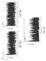
- FIG. 11A a time domain graph of pre-filtered output over time exemplary of an embodiment of the present invention is shown.
- An accurate time signal switching between positive 10 and negative 10 is indicated at approximately each cycle of approximately 17 nsec for system 200 to create the time domain waveform.
- FIG. 11B a graph of spectral output over frequency indicating harmonics exemplary of an embodiment of the present invention is shown.
- system 200 primary signal 1110 at 30 MHz and 34 dBm is indicated as well as even harmonics along the lower curve and odd harmonics along the upper curve.
- 3 rd harmonic 1120 maintaining a dependent delta of minus 19.8 to a value of 14.3.
- FIG. 11C a graph of current supplied to the load from each half bridge over time exemplary of an embodiment of the present invention is shown. Matching a similar pattern as time signal in FIG. 11A , current of each system 200 H-bridge left 114 and right 124 cycles between plus and minus approximately 600 mA.
- system 200 may preferably produce an output power measured across the load of 2.6 watts with a supplied DC power of 3.4 watts to maintain a DC to RF efficiency of 77%.
- FIGS. 12A-12C graphs of an exemplary 2.5 watt outphasing bridge circuit time domain signal with a 256 QAM drive illustrative of an embodiment of the present invention is shown.
- System 200 input signal represented by FIG. 12A shows a well-defined amplitude with a continuously varying phase component hidden by the graphical RF waveform data.
- the ability of system 200 to recreate the signal is indicated in FIG. 12B with an accurate representation of the input signal of FIG. 12A recreated in FIG. 12B with an amplified voltage level.
- System 200 output power represented in FIG. 12C is also an accurate representation of the input signal showing the peak power levels vs. average power levels of the QAM signal.
- One goal of the present invention is an efficient power amplifier operating within a high peak to average power range of a specific system.
- FIG. 12C shows high peaks in the power of the system at approximately 1 msec, 18 msec, and a final peak at 27 msec while the average power of the system is near 1.5 watts.
- Embodiments of the present invention may operate at acceptable efficiency levels within this high peak to average power ratio requirement.
- FIG. 13 a graph of envelope output voltage over time exemplary of an embodiment of the present invention is shown.
- the envelope of the system 200 input signal is graphically represented alongside the envelope of the system 200 output signal. An accurate representation would be indicated by an exact overlay.
- system 200 output envelope is nearly identical to the system 200 input envelope.
- Adjacent Channel Power Ratio may include a measurement of output spectrum to determine linearity.
- System 200 ACPR of 37.848 indicates highly linear performance of the outphasing power amplifier.
- FIG. 15A a table of measured data of an outphasing amplifier exemplary of an embodiment of the present invention is shown.
- the dc-to-rf efficiency is measured at 74.1% at full power. Noteworthy in the data is how efficiency remains high as power output is reduced. The efficiency remains close to full performance from zero back-off to approximately six dB of back-off.
- System 200 capabilities may be desirable in wideband multi tone signals that typically have a peak-to-average ratio (PAR) from 3 to 6 dB. As power is backed off by 9 dB, system 200 may continue operation at nearly 50% efficiency.
- PAR peak-to-average ratio
- FIG. 15B a combined graph of efficiency (%) and power out (W) over power back off exemplary of an embodiment of the present invention is shown. As indicated in tabular form above, the system 200 efficiency maintains above 60% to below 6 dB of back-off and just fewer than 50% at 9 dB of back-off.
- Efficiency may be one crucial characteristic for performance of an amplifier configured with an embodiment of the present invention.
- embodiments of the present invention may be configured for function within 256 QAM wideband HF radio applications.
- embodiments of the present invention may be configured within a small form factor handheld radio.
- applications maintaining high peak to average ratios requiring long life operation may successfully function with embodiments of the present invention included therein.
- a conventional single sideband amplifier commonly used in the HF realm may benefit from linearity advantages of embodiments herein.
- FIG. 16A a graph of AM to AM distortion indicative of a linear power amplifier exemplary of an embodiment of the present invention is shown.
- the AM-to-AM plot shows that the PA remains fairly linear as power is backed down from full output. However, at lower levels, linearity starts to rapidly degrade.
- FIG. 16B a graph of AM to PM distortion showing phase in degrees over input power in dB exemplary of an embodiment of the present invention is shown.
- System 200 distortion results in over 70 degrees through the amplifier at full output. It is contemplated herein; pre-distortion may be added at the input of the amplifier to correct for this and improve linearity.
- Method 1700 begins at step 1702 with transmitting a RF delay line frequency information, the RF delay line frequency information based on a radio frequency (RF) input, and, at step 1704 , transmitting a phase lock signal, the phase lock signal based on the RF input and a forward directional RF output signal, and, at step 1706 , transmitting a first RF delay control signal, the first RF delay control signal based on the phase lock signal and a reference current, and, at step 1708 , transmitting a second RF delay control signal, the second RF delay control signal based on a filtered RF input and a forward directional RF output signal, and, at step 1710 , shifting the phase of the RF input from zero degrees to one hundred eighty degrees based on the RF delay line frequency information and the first RF delay control signal, and, at step 1710 , shifting the phase of the RF input from zero degrees to one hundred eighty degrees based on the RF delay line frequency information and the first RF delay control signal, and, at
Abstract
Description
Claims (19)
Priority Applications (1)
| Application Number | Priority Date | Filing Date | Title |
|---|---|---|---|
| US13/901,790 US8963636B1 (en) | 2013-05-24 | 2013-05-24 | Outphasing power amplifier linearization method with improved output power back-off efficiency |
Applications Claiming Priority (1)
| Application Number | Priority Date | Filing Date | Title |
|---|---|---|---|
| US13/901,790 US8963636B1 (en) | 2013-05-24 | 2013-05-24 | Outphasing power amplifier linearization method with improved output power back-off efficiency |
Publications (1)
| Publication Number | Publication Date |
|---|---|
| US8963636B1 true US8963636B1 (en) | 2015-02-24 |
Family
ID=52472965
Family Applications (1)
| Application Number | Title | Priority Date | Filing Date |
|---|---|---|---|
| US13/901,790 Active 2033-08-23 US8963636B1 (en) | 2013-05-24 | 2013-05-24 | Outphasing power amplifier linearization method with improved output power back-off efficiency |
Country Status (1)
| Country | Link |
|---|---|
| US (1) | US8963636B1 (en) |
-
2013
- 2013-05-24 US US13/901,790 patent/US8963636B1/en active Active
Similar Documents
| Publication | Publication Date | Title |
|---|---|---|
| EP1636902B1 (en) | Power control for a transmitter | |
| EP1949638B1 (en) | Transmission circuit and communication apparatus employing the same | |
| US20080111622A1 (en) | Hybrid Doherty Amplifier System and Method | |
| US20070018718A1 (en) | Microwave transmitter and the method for increasing envelope bandwidth | |
| EP1262018A2 (en) | High-efficiency power modulators | |
| GB2498391A (en) | An envelope-tracking amplifier with signal predistortion and envelope shaping | |
| CN1332923A (en) | Power 1-Q modulation systems and methods | |
| JP4199680B2 (en) | Transmitter | |
| JP2005117599A (en) | High frequency amplifier | |
| Chung et al. | Asymmetric multilevel outphasing transmitter using class-E PAs with discrete pulse width modulation | |
| SE541265C2 (en) | Extended bandwidth digital doherty transmitter | |
| US8884697B2 (en) | Amplifying device | |
| JP2009260658A (en) | Power amplifier | |
| US8054878B2 (en) | Apparatus and method for amplifying signal power in a communication system | |
| WO2012023624A4 (en) | Chireix power amplification method and transmitter using envelope-tracking power supply | |
| WO2015055242A1 (en) | Amplifier apparatus and method | |
| WO2013115039A1 (en) | Power supply device and transmission device using same | |
| TWI390839B (en) | Distortion correction device and method for power amplifier | |
| US20150222230A1 (en) | Output power tuning using pulse position and pulse width control in a pulse position, pulse width modulation amplifier | |
| JP2017527191A (en) | Amplifier circuit and method for amplifying a signal using said amplifier circuit | |
| US8963636B1 (en) | Outphasing power amplifier linearization method with improved output power back-off efficiency | |
| Tajima et al. | Improved efficiency in outphasing power amplifier by mixing outphasing and amplitude modulation | |
| KR101358096B1 (en) | Power amplifier | |
| JP2011101111A (en) | Amplification device | |
| KR101686351B1 (en) | 3-way doherty power amplifier |
Legal Events
| Date | Code | Title | Description |
|---|---|---|---|
| AS | Assignment |
Owner name: ROCKWELL COLLINS, INC., IOWA Free format text: ASSIGNMENT OF ASSIGNORS INTEREST;ASSIGNORS:KRETT, DAVID L.;KEAN, TIMOTHY L.;HEGAZI, GAMAL M.;AND OTHERS;REEL/FRAME:030481/0269 Effective date: 20130523 |
|
| STCF | Information on status: patent grant |
Free format text: PATENTED CASE |
|
| MAFP | Maintenance fee payment |
Free format text: PAYMENT OF MAINTENANCE FEE, 4TH YEAR, LARGE ENTITY (ORIGINAL EVENT CODE: M1551); ENTITY STATUS OF PATENT OWNER: LARGE ENTITY Year of fee payment: 4 |
|
| MAFP | Maintenance fee payment |
Free format text: PAYMENT OF MAINTENANCE FEE, 8TH YEAR, LARGE ENTITY (ORIGINAL EVENT CODE: M1552); ENTITY STATUS OF PATENT OWNER: LARGE ENTITY Year of fee payment: 8 |