US8961196B2 - Electrical connector and a printed circuit board formed in said electrical connector - Google Patents
Electrical connector and a printed circuit board formed in said electrical connector Download PDFInfo
- Publication number
- US8961196B2 US8961196B2 US13/919,794 US201313919794A US8961196B2 US 8961196 B2 US8961196 B2 US 8961196B2 US 201313919794 A US201313919794 A US 201313919794A US 8961196 B2 US8961196 B2 US 8961196B2
- Authority
- US
- United States
- Prior art keywords
- contacts
- grounding
- electrical connector
- differential signal
- circuit board
- Prior art date
- Legal status (The legal status is an assumption and is not a legal conclusion. Google has not performed a legal analysis and makes no representation as to the accuracy of the status listed.)
- Active, expires
Links
Images


Classifications
-
- H—ELECTRICITY
- H01—ELECTRIC ELEMENTS
- H01R—ELECTRICALLY-CONDUCTIVE CONNECTIONS; STRUCTURAL ASSOCIATIONS OF A PLURALITY OF MUTUALLY-INSULATED ELECTRICAL CONNECTING ELEMENTS; COUPLING DEVICES; CURRENT COLLECTORS
- H01R13/00—Details of coupling devices of the kinds covered by groups H01R12/70 or H01R24/00 - H01R33/00
- H01R13/66—Structural association with built-in electrical component
- H01R13/665—Structural association with built-in electrical component with built-in electronic circuit
- H01R13/6658—Structural association with built-in electrical component with built-in electronic circuit on printed circuit board
-
- H—ELECTRICITY
- H05—ELECTRIC TECHNIQUES NOT OTHERWISE PROVIDED FOR
- H05K—PRINTED CIRCUITS; CASINGS OR CONSTRUCTIONAL DETAILS OF ELECTRIC APPARATUS; MANUFACTURE OF ASSEMBLAGES OF ELECTRICAL COMPONENTS
- H05K1/00—Printed circuits
- H05K1/02—Details
- H05K1/0213—Electrical arrangements not otherwise provided for
- H05K1/0254—High voltage adaptations; Electrical insulation details; Overvoltage or electrostatic discharge protection ; Arrangements for regulating voltages or for using plural voltages
- H05K1/0257—Overvoltage protection
- H05K1/0259—Electrostatic discharge [ESD] protection
-
- H—ELECTRICITY
- H05—ELECTRIC TECHNIQUES NOT OTHERWISE PROVIDED FOR
- H05K—PRINTED CIRCUITS; CASINGS OR CONSTRUCTIONAL DETAILS OF ELECTRIC APPARATUS; MANUFACTURE OF ASSEMBLAGES OF ELECTRICAL COMPONENTS
- H05K1/00—Printed circuits
- H05K1/02—Details
- H05K1/11—Printed elements for providing electric connections to or between printed circuits
- H05K1/117—Pads along the edge of rigid circuit boards, e.g. for pluggable connectors
-
- H—ELECTRICITY
- H05—ELECTRIC TECHNIQUES NOT OTHERWISE PROVIDED FOR
- H05K—PRINTED CIRCUITS; CASINGS OR CONSTRUCTIONAL DETAILS OF ELECTRIC APPARATUS; MANUFACTURE OF ASSEMBLAGES OF ELECTRICAL COMPONENTS
- H05K2201/00—Indexing scheme relating to printed circuits covered by H05K1/00
- H05K2201/09—Shape and layout
- H05K2201/09145—Edge details
- H05K2201/09154—Bevelled, chamferred or tapered edge
-
- H—ELECTRICITY
- H05—ELECTRIC TECHNIQUES NOT OTHERWISE PROVIDED FOR
- H05K—PRINTED CIRCUITS; CASINGS OR CONSTRUCTIONAL DETAILS OF ELECTRIC APPARATUS; MANUFACTURE OF ASSEMBLAGES OF ELECTRICAL COMPONENTS
- H05K2201/00—Indexing scheme relating to printed circuits covered by H05K1/00
- H05K2201/09—Shape and layout
- H05K2201/09209—Shape and layout details of conductors
- H05K2201/09372—Pads and lands
- H05K2201/09481—Via in pad; Pad over filled via
-
- H—ELECTRICITY
- H05—ELECTRIC TECHNIQUES NOT OTHERWISE PROVIDED FOR
- H05K—PRINTED CIRCUITS; CASINGS OR CONSTRUCTIONAL DETAILS OF ELECTRIC APPARATUS; MANUFACTURE OF ASSEMBLAGES OF ELECTRICAL COMPONENTS
- H05K2201/00—Indexing scheme relating to printed circuits covered by H05K1/00
- H05K2201/09—Shape and layout
- H05K2201/09209—Shape and layout details of conductors
- H05K2201/095—Conductive through-holes or vias
- H05K2201/09618—Via fence, i.e. one-dimensional array of vias
Definitions
- the present invention generally relates to an electrical connector and a printed circuit board formed in said electrical connector, more specifically to an electrical connector with high signal transmitting rate.
- U.S. Pat. No. 7,114,980 issued to Wu on Oct. 3, 2006 discloses an electrical connector comprising a metallic housing, a printed circuit board received into the housing.
- the printed circuit board defines a plurality of conductive pads respectively formed on top and bottom surfaces of a front and rear ends thereof.
- the plurality of conductive pads comprises a plurality of grounding contacts and a plurality of pairs of differential signal contacts. Two adjacent pairs of differential signal contacts are spaced apart by a grounding contact.
- U.S. Published. No. 20110256776 published to Reed on Oct. 20, 2011 also discloses an electrical connector with a printed circuit board formed therein.
- the printed circuit board defines several pairs of differential signal contacts and a plurality of grounding contact intervened between two adjacent differential signal contacts.
- the printed circuit board further defines two short conductive pads respectively located in front of each of the pair of differential signal contacts for preventing electrostatic discharge (ESD).
- ESD electrostatic discharge
- an object of the present invention is to provide an electrical connector with improved printed circuit board for preventing electrostatic discharge (ESD).
- an electrical connector comprises: a metallic housing; and a printed circuit board receiving in the metallic housing and defining a mating portion formed on a front end thereof.
- the mating portion defines a plurality of conductive pads formed on a top surface thereof, the plurality of conductive pads comprises a plurality of first grounding contacts, a plurality of pairs of differential signal contacts and a plurality of second grounding contacts, each of pair of differential signal contacts are intervened between two adjacent grounding contacts, each of second grounding contact is located in front of the pair of differential signal contacts and electrically and mechanically connected with two front ends of two first grounding contacts.
- FIG. 1 is a perspective view of an electrical connector in accordance with the present invention
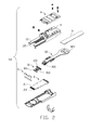
- FIG. 2 is an exploded, perspective view of FIG. 1 ;
- FIG. 3 is an enlarge perspective view of the printed circuit board shown in FIG. 2 ;
- FIG. 4 is an enlarge perspective view of an oval-shaped circle shown in FIG. 3 .
- FIG. 1 illustrate perspective view of an electrical connector 100 made in accordance with the present invention.
- the electrical connector 100 comprises a metallic housing 1 , a printed circuit board 2 received into the housing 1 , a latch mechanism 3 assembled to an exterior surface of the housing 1 , a metallic shell 4 shielding a portion of the latch mechanism 3 and a gasket 5 surrounding the metallic housing 1 .
- the metallic housing 1 defines a body portion 11 and a mating portion 12 extending forwardly from the body portion 11 .
- the metallic housing 1 defines a receiving room 120 formed therein.
- the printed circuit board 2 is received into the receiving room 120 of the housing 1 and extending along a longitudinal direction.
- the printed circuit board 2 defines a front mating portion 21 with a plurality of conductive pads 23 formed on opposite top and bottom surfaces thereof.
- the plurality of conductive pads 23 comprises a plurality of first grounding contacts 231 extending along a longitudinal direction, a plurality of pairs of differential signal contacts 230 extending along a longitudinal direction and a plurality of second grounding contacts 232 extending along a transversal direction. Each pair of differential signal contacts 230 are intervened between two adjacent first grounding contacts 231 .
- Each of the second grounding contact 231 is located in front of a pair of differential signal contacts 230 and is electrically and mechanically connected with two front ends 2310 of two first grounding contacts 231 located at two sides of the pair of differential signal contacts 230 .
- the front end 2310 of each first grounding contact 231 is located in front of a front end (not labeled) of each signal contact 230 .
- the front end 2310 of the first grounding contact 231 is located more closer to a front edge of of the printed circuit board 2 than the front end of the signal contacts 230 to the front edge of the printed circuit board 2 .
- the printed circuit board 2 further defines a plurality of through holes 2320 extending along a vertical direction throughout top and bottom surfaces thererof.
- Each of two through holes 2320 extends from top surface of the second grounding contact 232 to bottom surface of the printed circuit board 2 . Due to the through holes 2320 existed on the second grouding contacts 232 , the second grounding contacts 232 will not easily to be peeled when the electrical connector 100 is mated with the complemenatry connector (not shown). In addition, the first and second grounding contacts 231 are electrically connected to inner grounding layer (not shown) of the printed circuit board 2 .
- the latch mechanism 3 comprises a latching member 31 and a pulling member 32 connected with each other and assembled to the base portion 11 of the housing 1 together.
- the pulling member 32 is discrete from the latching member 31 and capable of moving along a front to rear direction relative to the housing 1 .
- the latch mechanism 3 further comprises a tape 9 connected to the pulling member 32 .
- the pulling member 324 comprises a rear operating portion 324 and a front actuating portion 321 attached to the latching member 31 .
- the latching member 31 comprises an engaging portion 310 engaged to the base portion 11 , an inclined middle portion 312 cooperated with the actuating portion 321 and a latching portion 311 located above the mating portion 12 .
- the first and second grounding contacts 231 , 232 are electrically connected with each other and arranged in a common grounding line.
- grounding contact therebetween will be occurred firstly.
- static electricity will be leaded into earth in a shortest time.
- electrostatic discharge (ESD) will be effective prevented when the electrical connector is mated with the complementary connector.
Landscapes
- Engineering & Computer Science (AREA)
- Microelectronics & Electronic Packaging (AREA)
- Details Of Connecting Devices For Male And Female Coupling (AREA)
- Coupling Device And Connection With Printed Circuit (AREA)
Abstract
Description
Claims (4)
Applications Claiming Priority (3)
| Application Number | Priority Date | Filing Date | Title |
|---|---|---|---|
| CN201210198300.6 | 2012-06-16 | ||
| CN201210198300 | 2012-06-16 | ||
| CN201210198300.6A CN103515793A (en) | 2012-06-16 | 2012-06-16 | Electric connector and printed circuit board contained in electric connector |
Publications (2)
| Publication Number | Publication Date |
|---|---|
| US20130337689A1 US20130337689A1 (en) | 2013-12-19 |
| US8961196B2 true US8961196B2 (en) | 2015-02-24 |
Family
ID=49756308
Family Applications (1)
| Application Number | Title | Priority Date | Filing Date |
|---|---|---|---|
| US13/919,794 Active 2033-07-03 US8961196B2 (en) | 2012-06-16 | 2013-06-17 | Electrical connector and a printed circuit board formed in said electrical connector |
Country Status (2)
| Country | Link |
|---|---|
| US (1) | US8961196B2 (en) |
| CN (1) | CN103515793A (en) |
Cited By (3)
| Publication number | Priority date | Publication date | Assignee | Title |
|---|---|---|---|---|
| US20160363731A1 (en) * | 2015-06-09 | 2016-12-15 | Commscope Technologies Llc | Device for transitioning from trunk cable to jumper cable |
| US10502915B2 (en) | 2017-06-29 | 2019-12-10 | Commscope Technologies Llc | Device for distributing trunk cable to jumper cable |
| US10916887B2 (en) * | 2019-05-08 | 2021-02-09 | Foxconn Interconnect Technology Limited | Plug connector having a housing module with two housings interlocked by deformed tongue having two legs |
Families Citing this family (1)
| Publication number | Priority date | Publication date | Assignee | Title |
|---|---|---|---|---|
| CN104979717B (en) * | 2015-04-16 | 2017-11-17 | 凡甲电子(苏州)有限公司 | Electric connector |
Citations (6)
| Publication number | Priority date | Publication date | Assignee | Title |
|---|---|---|---|---|
| US4532419A (en) * | 1982-09-09 | 1985-07-30 | Sony Corporation | Memory card having static electricity protection |
| US7114980B1 (en) | 2005-08-11 | 2006-10-03 | Hon Hai Precision Ind. Co., Ltd | Cable connector assembly with latching mechanism |
| US7803010B1 (en) * | 2010-02-11 | 2010-09-28 | Mao-Lin Hwang | Signal line connector structure of computer system |
| US8007294B2 (en) * | 2008-02-20 | 2011-08-30 | Japan Aviation Electronics Industry Limited | Connector |
| US20110256776A1 (en) | 2008-09-09 | 2011-10-20 | Molex Incorporated | Horizontally configured connector with edge card mounting structure |
| US8292655B1 (en) * | 2011-04-01 | 2012-10-23 | Intel Corporation | Innovative cable termination scheme |
Family Cites Families (2)
| Publication number | Priority date | Publication date | Assignee | Title |
|---|---|---|---|---|
| CN201051600Y (en) * | 2007-06-14 | 2008-04-23 | 青岛海信电器股份有限公司 | Circuit board hot swap interface |
| CN202231244U (en) * | 2011-08-19 | 2012-05-23 | 富士康(昆山)电脑接插件有限公司 | Electric connector |
-
2012
- 2012-06-16 CN CN201210198300.6A patent/CN103515793A/en active Pending
-
2013
- 2013-06-17 US US13/919,794 patent/US8961196B2/en active Active
Patent Citations (6)
| Publication number | Priority date | Publication date | Assignee | Title |
|---|---|---|---|---|
| US4532419A (en) * | 1982-09-09 | 1985-07-30 | Sony Corporation | Memory card having static electricity protection |
| US7114980B1 (en) | 2005-08-11 | 2006-10-03 | Hon Hai Precision Ind. Co., Ltd | Cable connector assembly with latching mechanism |
| US8007294B2 (en) * | 2008-02-20 | 2011-08-30 | Japan Aviation Electronics Industry Limited | Connector |
| US20110256776A1 (en) | 2008-09-09 | 2011-10-20 | Molex Incorporated | Horizontally configured connector with edge card mounting structure |
| US7803010B1 (en) * | 2010-02-11 | 2010-09-28 | Mao-Lin Hwang | Signal line connector structure of computer system |
| US8292655B1 (en) * | 2011-04-01 | 2012-10-23 | Intel Corporation | Innovative cable termination scheme |
Cited By (4)
| Publication number | Priority date | Publication date | Assignee | Title |
|---|---|---|---|---|
| US20160363731A1 (en) * | 2015-06-09 | 2016-12-15 | Commscope Technologies Llc | Device for transitioning from trunk cable to jumper cable |
| US10502915B2 (en) | 2017-06-29 | 2019-12-10 | Commscope Technologies Llc | Device for distributing trunk cable to jumper cable |
| US10698170B2 (en) | 2017-06-29 | 2020-06-30 | Commscope Technologies Llc | Device for distributing trunk cable to jumper cable |
| US10916887B2 (en) * | 2019-05-08 | 2021-02-09 | Foxconn Interconnect Technology Limited | Plug connector having a housing module with two housings interlocked by deformed tongue having two legs |
Also Published As
| Publication number | Publication date |
|---|---|
| US20130337689A1 (en) | 2013-12-19 |
| CN103515793A (en) | 2014-01-15 |
Similar Documents
| Publication | Publication Date | Title |
|---|---|---|
| US10236638B2 (en) | Electrical connector having separate grounding pieces | |
| US9627817B2 (en) | Electrical connector having a good high frequency transmission performance | |
| US9385482B2 (en) | Electrical connector with grounding plate | |
| US9059543B2 (en) | Cable connector assembly having a shell contacting a grounding pad of an internal printed circuit board | |
| US8764488B2 (en) | Connector having bridge member for coupling ground terminals | |
| US9917405B2 (en) | Electrical connector with central shield | |
| US9437980B2 (en) | Connector | |
| US9502827B2 (en) | Electrical connector with improved metal shell | |
| US9825407B2 (en) | Cable connector assembly having improved metal shell | |
| US10103501B2 (en) | Electrical connector with better ant-EMI effect | |
| TWI558006B (en) | First and second connectors mating with each other | |
| US8251746B2 (en) | Shielded electrical connector | |
| US10153596B2 (en) | Shielded electrical connector having two grounding members each with a plurality of contacting arms | |
| US20160056583A1 (en) | Electrical connector having improved housing and method of making the same | |
| US9490585B2 (en) | Electrical connector with imprived grounding bar | |
| US9419377B2 (en) | Dual orientation electrical connector assembly | |
| US9431769B2 (en) | Electrical connector having improved shielding | |
| US9698540B2 (en) | Cable connector assembly having internal metallic shield | |
| JP2011159470A (en) | Male connector, female connector, and connector | |
| US8961196B2 (en) | Electrical connector and a printed circuit board formed in said electrical connector | |
| US20140206231A1 (en) | Electrical connector with improved terminals | |
| TWM505730U (en) | Connector | |
| US20100317220A1 (en) | Electrical connector having grounding device | |
| JP2015018714A (en) | Connector | |
| US9124036B2 (en) | Electrical connector with improved grounding member for cross-talk prevention |
Legal Events
| Date | Code | Title | Description |
|---|---|---|---|
| AS | Assignment |
Owner name: HON HAI PRECISION INDUSTRY CO., LTD., TAIWAN Free format text: ASSIGNMENT OF ASSIGNORS INTEREST;ASSIGNORS:WU, JERRY;WANG, CHIEN-CHIUNG;CHEN, JUN;AND OTHERS;REEL/FRAME:030627/0164 Effective date: 20130606 |
|
| STCF | Information on status: patent grant |
Free format text: PATENTED CASE |
|
| MAFP | Maintenance fee payment |
Free format text: PAYMENT OF MAINTENANCE FEE, 4TH YEAR, LARGE ENTITY (ORIGINAL EVENT CODE: M1551); ENTITY STATUS OF PATENT OWNER: LARGE ENTITY Year of fee payment: 4 |
|
| MAFP | Maintenance fee payment |
Free format text: PAYMENT OF MAINTENANCE FEE, 8TH YEAR, LARGE ENTITY (ORIGINAL EVENT CODE: M1552); ENTITY STATUS OF PATENT OWNER: LARGE ENTITY Year of fee payment: 8 |