US8946720B2 - Organic light emitting diode display device and method of manufacturing the same - Google Patents
Organic light emitting diode display device and method of manufacturing the same Download PDFInfo
- Publication number
- US8946720B2 US8946720B2 US12/980,540 US98054010A US8946720B2 US 8946720 B2 US8946720 B2 US 8946720B2 US 98054010 A US98054010 A US 98054010A US 8946720 B2 US8946720 B2 US 8946720B2
- Authority
- US
- United States
- Prior art keywords
- layer
- electrode
- substrate
- light emitting
- emitting diode
- Prior art date
- Legal status (The legal status is an assumption and is not a legal conclusion. Google has not performed a legal analysis and makes no representation as to the accuracy of the status listed.)
- Active, expires
Links
- 238000004519 manufacturing process Methods 0.000 title abstract description 10
- 239000000758 substrate Substances 0.000 claims abstract description 36
- 239000004065 semiconductor Substances 0.000 claims abstract description 21
- 125000006850 spacer group Chemical group 0.000 claims abstract description 19
- 239000010410 layer Substances 0.000 claims description 148
- 229910052581 Si3N4 Inorganic materials 0.000 claims description 20
- HQVNEWCFYHHQES-UHFFFAOYSA-N silicon nitride Chemical compound N12[Si]34N5[Si]62N3[Si]51N64 HQVNEWCFYHHQES-UHFFFAOYSA-N 0.000 claims description 20
- 239000000463 material Substances 0.000 claims description 17
- 229910052751 metal Inorganic materials 0.000 claims description 10
- 239000002184 metal Substances 0.000 claims description 10
- 239000012044 organic layer Substances 0.000 claims description 10
- 239000004952 Polyamide Substances 0.000 claims description 6
- 239000004642 Polyimide Substances 0.000 claims description 6
- UMIVXZPTRXBADB-UHFFFAOYSA-N benzocyclobutene Chemical compound C1=CC=C2CCC2=C1 UMIVXZPTRXBADB-UHFFFAOYSA-N 0.000 claims description 6
- 229920002647 polyamide Polymers 0.000 claims description 6
- 229920001721 polyimide Polymers 0.000 claims description 6
- VYPSYNLAJGMNEJ-UHFFFAOYSA-N Silicium dioxide Chemical compound O=[Si]=O VYPSYNLAJGMNEJ-UHFFFAOYSA-N 0.000 claims description 5
- 229910052814 silicon oxide Inorganic materials 0.000 claims description 5
- 239000004925 Acrylic resin Substances 0.000 claims description 4
- 229920000178 Acrylic resin Polymers 0.000 claims description 4
- 239000005011 phenolic resin Substances 0.000 claims description 4
- 239000000203 mixture Substances 0.000 claims description 2
- 229910052710 silicon Inorganic materials 0.000 claims 1
- 239000010703 silicon Substances 0.000 claims 1
- 125000000123 silicon containing inorganic group Chemical group 0.000 claims 1
- 238000000034 method Methods 0.000 description 8
- 229910052782 aluminium Inorganic materials 0.000 description 3
- 239000010408 film Substances 0.000 description 3
- 229910052738 indium Inorganic materials 0.000 description 3
- APFVFJFRJDLVQX-UHFFFAOYSA-N indium atom Chemical compound [In] APFVFJFRJDLVQX-UHFFFAOYSA-N 0.000 description 3
- 229910000838 Al alloy Inorganic materials 0.000 description 2
- ZOKXTWBITQBERF-UHFFFAOYSA-N Molybdenum Chemical compound [Mo] ZOKXTWBITQBERF-UHFFFAOYSA-N 0.000 description 2
- 229910004205 SiNX Inorganic materials 0.000 description 2
- 229910045601 alloy Inorganic materials 0.000 description 2
- 239000000956 alloy Substances 0.000 description 2
- XAGFODPZIPBFFR-UHFFFAOYSA-N aluminium Chemical compound [Al] XAGFODPZIPBFFR-UHFFFAOYSA-N 0.000 description 2
- UBSJOWMHLJZVDJ-UHFFFAOYSA-N aluminum neodymium Chemical compound [Al].[Nd] UBSJOWMHLJZVDJ-UHFFFAOYSA-N 0.000 description 2
- 238000005229 chemical vapour deposition Methods 0.000 description 2
- 230000007423 decrease Effects 0.000 description 2
- 238000005530 etching Methods 0.000 description 2
- 239000011521 glass Substances 0.000 description 2
- 229910052750 molybdenum Inorganic materials 0.000 description 2
- 239000011733 molybdenum Substances 0.000 description 2
- 239000011368 organic material Substances 0.000 description 2
- 238000005240 physical vapour deposition Methods 0.000 description 2
- 239000004033 plastic Substances 0.000 description 2
- 239000000126 substance Substances 0.000 description 2
- QGZKDVFQNNGYKY-UHFFFAOYSA-O Ammonium Chemical compound [NH4+] QGZKDVFQNNGYKY-UHFFFAOYSA-O 0.000 description 1
- VYZAMTAEIAYCRO-UHFFFAOYSA-N Chromium Chemical compound [Cr] VYZAMTAEIAYCRO-UHFFFAOYSA-N 0.000 description 1
- BLRPTPMANUNPDV-UHFFFAOYSA-N Silane Chemical compound [SiH4] BLRPTPMANUNPDV-UHFFFAOYSA-N 0.000 description 1
- 229910008814 WSi2 Inorganic materials 0.000 description 1
- YXTPWUNVHCYOSP-UHFFFAOYSA-N bis($l^{2}-silanylidene)molybdenum Chemical compound [Si]=[Mo]=[Si] YXTPWUNVHCYOSP-UHFFFAOYSA-N 0.000 description 1
- 230000005283 ground state Effects 0.000 description 1
- AMGQUBHHOARCQH-UHFFFAOYSA-N indium;oxotin Chemical compound [In].[Sn]=O AMGQUBHHOARCQH-UHFFFAOYSA-N 0.000 description 1
- MGRWKWACZDFZJT-UHFFFAOYSA-N molybdenum tungsten Chemical compound [Mo].[W] MGRWKWACZDFZJT-UHFFFAOYSA-N 0.000 description 1
- 238000000059 patterning Methods 0.000 description 1
- 238000000206 photolithography Methods 0.000 description 1
- 229910000077 silane Inorganic materials 0.000 description 1
- 229910052709 silver Inorganic materials 0.000 description 1
- 239000002356 single layer Substances 0.000 description 1
- 239000010409 thin film Substances 0.000 description 1
- WFKWXMTUELFFGS-UHFFFAOYSA-N tungsten Chemical compound [W] WFKWXMTUELFFGS-UHFFFAOYSA-N 0.000 description 1
- 229910052721 tungsten Inorganic materials 0.000 description 1
- 239000010937 tungsten Substances 0.000 description 1
- WQJQOUPTWCFRMM-UHFFFAOYSA-N tungsten disilicide Chemical compound [Si]#[W]#[Si] WQJQOUPTWCFRMM-UHFFFAOYSA-N 0.000 description 1
- 229910021342 tungsten silicide Inorganic materials 0.000 description 1
- YVTHLONGBIQYBO-UHFFFAOYSA-N zinc indium(3+) oxygen(2-) Chemical compound [O--].[Zn++].[In+3] YVTHLONGBIQYBO-UHFFFAOYSA-N 0.000 description 1
Images


Classifications
-
- H—ELECTRICITY
- H10—SEMICONDUCTOR DEVICES; ELECTRIC SOLID-STATE DEVICES NOT OTHERWISE PROVIDED FOR
- H10K—ORGANIC ELECTRIC SOLID-STATE DEVICES
- H10K50/00—Organic light-emitting devices
- H10K50/80—Constructional details
- H10K50/805—Electrodes
- H10K50/81—Anodes
- H10K50/816—Multilayers, e.g. transparent multilayers
-
- H—ELECTRICITY
- H01—ELECTRIC ELEMENTS
- H01L—SEMICONDUCTOR DEVICES NOT COVERED BY CLASS H10
- H01L21/00—Processes or apparatus adapted for the manufacture or treatment of semiconductor or solid state devices or of parts thereof
- H01L21/02—Manufacture or treatment of semiconductor devices or of parts thereof
- H01L21/02104—Forming layers
- H01L21/02107—Forming insulating materials on a substrate
- H01L21/02109—Forming insulating materials on a substrate characterised by the type of layer, e.g. type of material, porous/non-porous, pre-cursors, mixtures or laminates
- H01L21/02112—Forming insulating materials on a substrate characterised by the type of layer, e.g. type of material, porous/non-porous, pre-cursors, mixtures or laminates characterised by the material of the layer
- H01L21/02123—Forming insulating materials on a substrate characterised by the type of layer, e.g. type of material, porous/non-porous, pre-cursors, mixtures or laminates characterised by the material of the layer the material containing silicon
- H01L21/0217—Forming insulating materials on a substrate characterised by the type of layer, e.g. type of material, porous/non-porous, pre-cursors, mixtures or laminates characterised by the material of the layer the material containing silicon the material being a silicon nitride not containing oxygen, e.g. SixNy or SixByNz
-
- H01L51/5215—
-
- H—ELECTRICITY
- H01—ELECTRIC ELEMENTS
- H01L—SEMICONDUCTOR DEVICES NOT COVERED BY CLASS H10
- H01L21/00—Processes or apparatus adapted for the manufacture or treatment of semiconductor or solid state devices or of parts thereof
- H01L21/02—Manufacture or treatment of semiconductor devices or of parts thereof
- H01L21/02104—Forming layers
- H01L21/02107—Forming insulating materials on a substrate
- H01L21/02109—Forming insulating materials on a substrate characterised by the type of layer, e.g. type of material, porous/non-porous, pre-cursors, mixtures or laminates
- H01L21/02112—Forming insulating materials on a substrate characterised by the type of layer, e.g. type of material, porous/non-porous, pre-cursors, mixtures or laminates characterised by the material of the layer
- H01L21/02123—Forming insulating materials on a substrate characterised by the type of layer, e.g. type of material, porous/non-porous, pre-cursors, mixtures or laminates characterised by the material of the layer the material containing silicon
- H01L21/02126—Forming insulating materials on a substrate characterised by the type of layer, e.g. type of material, porous/non-porous, pre-cursors, mixtures or laminates characterised by the material of the layer the material containing silicon the material containing Si, O, and at least one of H, N, C, F, or other non-metal elements, e.g. SiOC, SiOC:H or SiONC
- H01L21/0214—Forming insulating materials on a substrate characterised by the type of layer, e.g. type of material, porous/non-porous, pre-cursors, mixtures or laminates characterised by the material of the layer the material containing silicon the material containing Si, O, and at least one of H, N, C, F, or other non-metal elements, e.g. SiOC, SiOC:H or SiONC the material being a silicon oxynitride, e.g. SiON or SiON:H
-
- H01L27/3246—
-
- H—ELECTRICITY
- H10—SEMICONDUCTOR DEVICES; ELECTRIC SOLID-STATE DEVICES NOT OTHERWISE PROVIDED FOR
- H10K—ORGANIC ELECTRIC SOLID-STATE DEVICES
- H10K59/00—Integrated devices, or assemblies of multiple devices, comprising at least one organic light-emitting element covered by group H10K50/00
- H10K59/10—OLED displays
- H10K59/12—Active-matrix OLED [AMOLED] displays
- H10K59/122—Pixel-defining structures or layers, e.g. banks
-
- H—ELECTRICITY
- H10—SEMICONDUCTOR DEVICES; ELECTRIC SOLID-STATE DEVICES NOT OTHERWISE PROVIDED FOR
- H10K—ORGANIC ELECTRIC SOLID-STATE DEVICES
- H10K59/00—Integrated devices, or assemblies of multiple devices, comprising at least one organic light-emitting element covered by group H10K50/00
- H10K59/80—Constructional details
- H10K59/805—Electrodes
- H10K59/8051—Anodes
- H10K59/80517—Multilayers, e.g. transparent multilayers
-
- H01L2227/323—
-
- H—ELECTRICITY
- H10—SEMICONDUCTOR DEVICES; ELECTRIC SOLID-STATE DEVICES NOT OTHERWISE PROVIDED FOR
- H10K—ORGANIC ELECTRIC SOLID-STATE DEVICES
- H10K2102/00—Constructional details relating to the organic devices covered by this subclass
-
- H—ELECTRICITY
- H10—SEMICONDUCTOR DEVICES; ELECTRIC SOLID-STATE DEVICES NOT OTHERWISE PROVIDED FOR
- H10K—ORGANIC ELECTRIC SOLID-STATE DEVICES
- H10K59/00—Integrated devices, or assemblies of multiple devices, comprising at least one organic light-emitting element covered by group H10K50/00
- H10K59/10—OLED displays
- H10K59/12—Active-matrix OLED [AMOLED] displays
- H10K59/1201—Manufacture or treatment
Definitions
- the present invention relates generally to an organic light emitting diode display device and a method of manufacturing the same, to which a 5-mask process can be applied, thereby making it possible to reduce the number of masks, cut down the cost of production, and simplify a process to enhance a yield.
- organic light emitting diode display devices exhibit characteristics such as self-emission, wide viewing angle, rapid response speed of 1 ms or less, thin thickness, low manufacturing cost, and high contrast.
- the organic light emitting diode display devices includes an organic emission layer between a positive electrode (anode) and a negative electrode (cathode).
- anode positive electrode
- cathode negative electrode
- holes supplied from the anode and electrons supplied from the cathode are combined in the organic emission layer, thereby forming hole-electron pairs, i.e. excitons.
- the excitons release energy while returning to a ground state so that light is emitted.
- the organic light emitting diode display devices are generally configured to mount a thin film transistor on each pixel, and supply constant current regardless of the number of pixels, so that they can provide stable luminance and low power consumption, and thus they are advantageous for application to high-resolution and large displays.
- the present invention provides an organic light emitting diode display device which is capable of reducing the number of masks so as to cut down the cost of production and enhance a yield, and a method of manufacturing the same.
- the present invention also provides an organic light emitting diode display device including: a substrate having an emission section and a non-emission section; a semiconductor layer located on the substrate; a gate dielectric layer located on an entire front surface of the substrate; a gate electrode located in correspondence to the semiconductor layer; a dielectric layer located on an entire front surface of the substrate; source and drain electrodes and a first electrode located on the dielectric layer and electrically connected to the semiconductor layer, the first electrode being located on the emission section of the substrate; a pixel definition layer exposing a part of the first electrode; a spacer located on the pixel definition layer and located on the non-emission section of the substrate; an organic film layer located on the first electrode; and a second electrode located on an entire front surface of the substrate.
- the pixel definition layer includes an inorganic layer, and the spacer includes an organic layer.
- FIGS. 1A thru 1 H illustrate an organic light emitting diode display device according to a first embodiment of the invention
- FIGS. 1I thru 1 L are microscopic photographs of a pixel electrode formed of a silicon nitride layer.
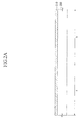
- FIGS. 2A thru 2 H illustrate an organic light emitting diode display device according to a second embodiment of the invention.
- FIGS. 1A thru 1 H illustrate an organic light emitting diode display device according to a first embodiment of the invention.
- a substrate 100 having an emission section a and non-emission section b is provided.
- the substrate 100 is formed of a material such as glass or plastic.
- a buffer layer 110 is formed on the substrate 100 .
- the buffer layer 110 is formed of at least one dielectric layer, for instance, a silicon oxide layer and a silicon nitride layer, using chemical or physical vapor deposition.
- a semiconductor layer 120 is formed on the buffer layer 110 using a first mask. Then, a gate dielectric layer 130 is formed over an entire front surface of the substrate 100 .
- the gate dielectric layer 130 may be formed of a silicon oxide layer, a silicon nitride layer or both of them.
- a gate electrode 140 is formed on the gate dielectric layer 130 so as to correspond to the semiconductor layer 120 .
- the gate electrode 140 is formed using a second mask.
- the gate electrode 140 is formed by forming a single layer of aluminum (Al) or an aluminum alloy such as aluminum-neodymium (Al—Nd), or a multiple layer in which an Al alloy is stacked on a chrome (Cr) or molybdenum (Mo) alloy as a metal layer (not shown) for the gate electrode, and etching the metal layer using a photolithography process.
- a dielectric layer 150 is formed above the substrate 100 so as to have contact holes A exposing parts of the semiconductor layer 120 .
- the dielectric layer 150 is formed using a third mask, and is formed using a mixture layer in which an inorganic layer such as a silicon nitride layer, a silicon oxide layer, or a multiple layer thereof is mixed with a planarization layer which is made of one selected from the group consisting of benzo cyclo butene (BCB), polyimide (PI), polyamide (PA), acrylic resin, and phenol resin, which are typically used as organic materials.
- BCB benzo cyclo butene
- PI polyimide
- PA polyamide
- acrylic resin acrylic resin
- phenol resin phenol resin
- source and drain electrodes 160 a and 160 b respectively, and a first electrode 170 are formed on the dielectric layer 150 so as to be electrically connected to the semiconductor layer 120 .
- the source and drain electrodes 160 a and 160 b and the first electrode 170 are simultaneously formed by stacking a metal layer (not shown) for the source and drain electrodes 160 a and 160 b , respectively, and a metal layer (not shown) for the first electrode 170 using a fourth mask.
- the metal layer for the source and drain electrodes 160 a and 160 b may be formed of one selected from molybdenum (Mo), tungsten (W), molybdenum tungsten (MoW), tungsten silicide (WSi 2 ), molybdenum silicide (MoSi2), and aluminum (Al).
- the metal layer for the first electrode 170 may be formed of one selected from layers including an indium tin oxide (ITO) layer, indium zinc oxide (IZO) layer, and a reflective layer.
- the reflective layer may be formed of Ag, Al or an alloy thereof.
- material layers for a pixel definition layer 173 and a spacer 175 are formed over an entire front surface of the substrate 100 .
- the material layer of the pixel definition layer 173 may be formed using an inorganic layer, preferably a silicon nitride (SiNx) layer.
- the material layer for the spacer 175 is formed of one selected from the group consisting of BCB, PI, PA, acrylic resin, and phenol resin, which are typical organic materials.
- the material layer, i.e. the organic layer, for the spacer 175 is ashed using a half-tone mask, a fifth mask, thereby removing a part of the organic layer located on the emission section a, so that an organic layer pattern is left on a part of the non-emission section b.
- the material layer, i.e. the inorganic layer, for the pixel definition layer 173 is dry-etched to expose a part of the first electrode 170 .
- a part of the material layer for the pixel definition layer 173 is removed by etching, and thus a part of the first electrode 170 located on the emission section is exposed, so that the pixel definition layer 173 defining a pixel is formed.
- the organic layer for the spacer 175 is ashed, so that the spacer 175 , i.e. the organic layer pattern, located on the non-emission section is formed.
- the pixel definition layer 173 is formed of the inorganic layer, it is possible to prevent the source and drain electrodes 160 a and 160 b , respectively, from being damaged, which is a problem occurring when the pixel definition layer 173 is formed of an organic layer and when the source and drain electrodes 160 a and 160 b , respectively, are formed parallel to the first electrode 170 .
- the pixel definition layer 173 and the spacer 175 are formed using one mask process, so that it is possible to produce a reliable device, and cut down the cost of production.
- the pixel definition layer 173 is formed using the inorganic layer, i.e. the silicon nitride (SiNx) layer, amounts of silane gas and ammonium gas are adjusted so that the silicon nitride layer contains 18 wt % or less of Si. This is because, when the pixel definition layer 173 is formed on the ITO electrode using the silicon nitride layer, and when the content of Si of the silicon nitride layer is high, indium (In) of the ITO electrode migrates to the silicon nitride layer, thereby influencing the pixel definition layer 173 , and thus characteristics of the device.
- SiNx silicon nitride
- FIGS. 1I thru 1 L are microscopic photographs of a pixel region coated with a silicon nitride layer, wherein FIG. 1I shows a case wherein the silicon nitride layer contains 47 wt % of Si, FIG. 1J shows a case wherein the silicon nitride layer contains 40 wt % of Si, FIG. 1K shows a case wherein the silicon nitride layer contains 31 wt % of Si, and FIG. 1L shows a case wherein the silicon nitride layer contains 18 wt % of Si.
- FIGS. 1I shows a case wherein the silicon nitride layer contains 47 wt % of Si
- FIG. 1J shows a case wherein the silicon nitride layer contains 40 wt % of Si
- FIG. 1K shows a case wherein the silicon nitride layer contains 31 wt % of Si
- FIG. 1L shows a case wherein the silicon nitride layer
- an organic film layer 180 including an organic emission layer is formed on the exposed first electrode 170 , and then a second electrode 190 is formed over the entire front surface of the substrate 100 . Thereby, the organic light emitting diode display device according to a first embodiment is finished.
- FIGS. 2A thru 2 H illustrate an organic light emitting diode display device according to a second embodiment of the invention.
- a substrate 200 having an emission section a and non-emission section b is provided.
- the substrate 200 is formed of a material such as glass or plastic.
- a buffer layer 210 is formed on the substrate 200 .
- the buffer layer 210 is formed of at least one of dielectric layers, for instance, a silicon oxide layer and a silicon nitride layer, using chemical or physical vapor deposition.
- a gate electrode 220 is formed on the substrate 200 using a first mask. Then, a gate dielectric layer 230 is formed over an entire front surface of the substrate 200 . The gate electrode 220 and the gate dielectric layer 230 are formed as in the first embodiment.
- a semiconductor layer 240 is formed on the gate dielectric layer 230 so as to correspond to the gate electrode 220 .
- the semiconductor layer 240 is formed using a second mask.
- an etch stop layer 250 is formed on the semiconductor layer 240 using a third mask so as to prevent damage to the semiconductor layer 240 . Then, source and drain electrodes 260 a and 260 b , respectively, and a first electrode 270 are formed using a fourth mask so as to be electrically connected to the semiconductor layer 240 .
- the source and drain electrodes 260 a and 260 b , respectively, and the first electrode 270 are formed by stacking and patterning a metal layer (not shown) for the source and drain electrodes 260 a and 260 b , respectively, and a metal layer (not shown) for the first electrode 270 , both of which are the same material, using the same mask at the same time.
- a contact layer 255 is located under the source and drain electrodes 260 a and 260 b , respectively, and the first electrode 270 .
- the contact layer 255 is interposed between the semiconductor layer 240 and the source and drain electrodes 260 a and 260 b , respectively.
- material layers for a pixel definition layer 273 and a spacer 275 are formed over an entire front surface of the substrate 200 .
- the material layer for the pixel definition layer 273 is formed of an inorganic layer, and the material layer for the spacer 275 is formed of an organic layer. In the same fashion as described in the first embodiment, the material layers for the pixel definition layer 273 and the spacer 275 are formed.
- the material layer for the spacer 275 is ashed using a fifth mask, thereby exposing a part of the emission section a of the substrate 200 .
- the fifth mask is the same mask, i.e. the half-tone mask, as described in the first embodiment, so that it is possible to adjust a degree to which the organic layer is ashed.
- the material layer, i.e. the inorganic layer, for the pixel definition layer 273 is etched to expose a part of the first electrode 270 .
- the pixel definition layer 273 defining a pixel and the spacer 275 located on the non-emission section b of the substrate 200 are formed.
- an organic film layer 280 including an organic emission layer is formed on the exposed first electrode 270 , and then a second electrode 290 is formed over the entire front surface of the substrate 100 . Thereby, the organic light emitting diode display device according to a second embodiment is finished.
- the positions of the gate electrode and the semiconductor layer are different.
- the materials applied to the semiconductor layer, the gate electrode, the source and drain electrodes, the first electrode, and the second electrode are the same as in the first embodiment.
- the organic light emitting diode display device is configured such that a pixel definition layer is formed of an optimized inorganic layer, and is simultaneously formed along with a spacer. As a result, it is possible to reduce the mask process and production time so as to cut down the cost of production, and to enhance yield.
Landscapes
- Engineering & Computer Science (AREA)
- Microelectronics & Electronic Packaging (AREA)
- Physics & Mathematics (AREA)
- Manufacturing & Machinery (AREA)
- Condensed Matter Physics & Semiconductors (AREA)
- General Physics & Mathematics (AREA)
- Computer Hardware Design (AREA)
- Power Engineering (AREA)
- Optics & Photonics (AREA)
- Electroluminescent Light Sources (AREA)
Abstract
Description
Claims (7)
Applications Claiming Priority (2)
| Application Number | Priority Date | Filing Date | Title |
|---|---|---|---|
| KR1020100001723A KR101119046B1 (en) | 2010-01-08 | 2010-01-08 | Organic light emitting display deviece and the fabricating method of the same |
| KR10-2010-0001723 | 2010-01-08 |
Publications (2)
| Publication Number | Publication Date |
|---|---|
| US20110168985A1 US20110168985A1 (en) | 2011-07-14 |
| US8946720B2 true US8946720B2 (en) | 2015-02-03 |
Family
ID=44257834
Family Applications (1)
| Application Number | Title | Priority Date | Filing Date |
|---|---|---|---|
| US12/980,540 Active 2032-11-04 US8946720B2 (en) | 2010-01-08 | 2010-12-29 | Organic light emitting diode display device and method of manufacturing the same |
Country Status (2)
| Country | Link |
|---|---|
| US (1) | US8946720B2 (en) |
| KR (1) | KR101119046B1 (en) |
Cited By (1)
| Publication number | Priority date | Publication date | Assignee | Title |
|---|---|---|---|---|
| US10950673B2 (en) | 2018-05-14 | 2021-03-16 | Samsung Display Co., Ltd. | Display device structure for reducing defects |
Families Citing this family (5)
| Publication number | Priority date | Publication date | Assignee | Title |
|---|---|---|---|---|
| KR20140033671A (en) | 2012-09-10 | 2014-03-19 | 삼성디스플레이 주식회사 | Organic light emitting diode display and method of fabricating the same |
| KR20140090458A (en) | 2013-01-09 | 2014-07-17 | 삼성디스플레이 주식회사 | Organic light emitting diode display and manufacturing method thereof |
| KR20170040425A (en) | 2015-10-02 | 2017-04-13 | 삼성디스플레이 주식회사 | Organic light emitting diode display and method for manufacturing the same |
| CN106449718B (en) * | 2016-11-15 | 2019-10-18 | 武汉华星光电技术有限公司 | Oled substrate and preparation method thereof |
| CN111554580B (en) * | 2020-05-14 | 2024-06-18 | 京东方科技集团股份有限公司 | Thin film transistor, manufacturing method thereof, display substrate and display device |
Citations (25)
| Publication number | Priority date | Publication date | Assignee | Title |
|---|---|---|---|---|
| KR20050105852A (en) | 2004-05-03 | 2005-11-08 | 삼성에스디아이 주식회사 | An active matrix organic electrominescence display and method for fabricating the same |
| KR20060018767A (en) | 2004-08-25 | 2006-03-02 | 삼성에스디아이 주식회사 | Organic electroluminescence display device and fabrication method of the same |
| US20070052352A1 (en) * | 2005-09-08 | 2007-03-08 | Samsung Sdi Co., Ltd. | Organic light emitting display device and method of fabricating the same |
| KR20070055908A (en) | 2005-11-28 | 2007-05-31 | 삼성에스디아이 주식회사 | Fabrication method of organic electro luminescence device |
| KR20070068092A (en) | 2005-12-26 | 2007-06-29 | 엘지.필립스 엘시디 주식회사 | The organic electro-luminescence device and method for fabricating of the same |
| US20070170839A1 (en) | 2006-01-20 | 2007-07-26 | Choi Dong S | Organic light-emitting display device with frit seal and reinforcing structure |
| KR20080014328A (en) | 2006-08-10 | 2008-02-14 | 삼성에스디아이 주식회사 | Organic light emitting display apparatus and method of manufacturing the same |
| KR20080047777A (en) | 2006-11-27 | 2008-05-30 | 삼성에스디아이 주식회사 | Organic light emitting display and method for manufacturing the same |
| US20080160864A1 (en) | 2007-01-03 | 2008-07-03 | Seung-Yong Song | Method for manufacturing organic light emitting display |
| US7420212B2 (en) * | 2003-11-28 | 2008-09-02 | Samsung Sdi Co., Ltd. | Flat panel display |
| US20080277666A1 (en) * | 2007-05-11 | 2008-11-13 | Hee-Chul Jeon | Thin film transistor, organic light emitting display device including the same, and method of manufacturing the organic light emitting display device |
| US7459850B2 (en) | 2005-06-22 | 2008-12-02 | Eastman Kodak Company | OLED device having spacers |
| US20080315756A1 (en) | 2007-06-20 | 2008-12-25 | Samsung Sdi Co., Ltd. | Organic light emitting display and manufacturing thereof |
| US20090008667A1 (en) * | 2007-06-19 | 2009-01-08 | Semiconductor Energy Laboratory Co., Ltd. | Method for forming pattern, method for manufacturing light emitting device, and light emitting device |
| US20090009055A1 (en) | 2007-07-04 | 2009-01-08 | Dong-Won Han | Organic light emitting display device and manufacturing method of the same |
| US20090058294A1 (en) | 2007-09-05 | 2009-03-05 | Young-Cheol Joo | Light emitting display device and method for fabricating the same |
| US7550769B2 (en) * | 2004-06-11 | 2009-06-23 | Semiconductor Energy Laboratory Co., Ltd. | Light emitting element, light emitting device and semiconductor device |
| US7557494B2 (en) | 2002-06-21 | 2009-07-07 | Hitachi Displays, Ltd. | Display device |
| US20090189517A1 (en) | 2008-01-30 | 2009-07-30 | Choi Young-Seo | Organic light emitting display and method for manufacturing the same |
| KR20090084202A (en) | 2008-01-31 | 2009-08-05 | 삼성모바일디스플레이주식회사 | Organic light emitting diode display and method for fabricating of the same |
| US7595854B2 (en) | 2006-09-04 | 2009-09-29 | Samsung Mobile Display Co., Ltd. | Organic light emitting display device |
| US7692381B2 (en) | 2006-02-10 | 2010-04-06 | Samsung Mobile Display Co., Ltd. | Organic light emitting display device with a metal substrate and method for fabricating the same |
| US20100097295A1 (en) | 2008-10-17 | 2010-04-22 | Won-Kyu Kwak | Organic light emitting display |
| US7749039B2 (en) | 2006-04-20 | 2010-07-06 | Samsung Mobile Display Co., Ltd. | Organic light emitting display device and method of manufacturing the same |
| US7777225B2 (en) | 2007-05-21 | 2010-08-17 | Samsung Mobile Display Co., Ltd. | Organic light-emitting display device |
-
2010
- 2010-01-08 KR KR1020100001723A patent/KR101119046B1/en active IP Right Grant
- 2010-12-29 US US12/980,540 patent/US8946720B2/en active Active
Patent Citations (25)
| Publication number | Priority date | Publication date | Assignee | Title |
|---|---|---|---|---|
| US7557494B2 (en) | 2002-06-21 | 2009-07-07 | Hitachi Displays, Ltd. | Display device |
| US7420212B2 (en) * | 2003-11-28 | 2008-09-02 | Samsung Sdi Co., Ltd. | Flat panel display |
| KR20050105852A (en) | 2004-05-03 | 2005-11-08 | 삼성에스디아이 주식회사 | An active matrix organic electrominescence display and method for fabricating the same |
| US7550769B2 (en) * | 2004-06-11 | 2009-06-23 | Semiconductor Energy Laboratory Co., Ltd. | Light emitting element, light emitting device and semiconductor device |
| KR20060018767A (en) | 2004-08-25 | 2006-03-02 | 삼성에스디아이 주식회사 | Organic electroluminescence display device and fabrication method of the same |
| US7459850B2 (en) | 2005-06-22 | 2008-12-02 | Eastman Kodak Company | OLED device having spacers |
| US20070052352A1 (en) * | 2005-09-08 | 2007-03-08 | Samsung Sdi Co., Ltd. | Organic light emitting display device and method of fabricating the same |
| KR20070055908A (en) | 2005-11-28 | 2007-05-31 | 삼성에스디아이 주식회사 | Fabrication method of organic electro luminescence device |
| KR20070068092A (en) | 2005-12-26 | 2007-06-29 | 엘지.필립스 엘시디 주식회사 | The organic electro-luminescence device and method for fabricating of the same |
| US20070170839A1 (en) | 2006-01-20 | 2007-07-26 | Choi Dong S | Organic light-emitting display device with frit seal and reinforcing structure |
| US7692381B2 (en) | 2006-02-10 | 2010-04-06 | Samsung Mobile Display Co., Ltd. | Organic light emitting display device with a metal substrate and method for fabricating the same |
| US7749039B2 (en) | 2006-04-20 | 2010-07-06 | Samsung Mobile Display Co., Ltd. | Organic light emitting display device and method of manufacturing the same |
| KR20080014328A (en) | 2006-08-10 | 2008-02-14 | 삼성에스디아이 주식회사 | Organic light emitting display apparatus and method of manufacturing the same |
| US7595854B2 (en) | 2006-09-04 | 2009-09-29 | Samsung Mobile Display Co., Ltd. | Organic light emitting display device |
| KR20080047777A (en) | 2006-11-27 | 2008-05-30 | 삼성에스디아이 주식회사 | Organic light emitting display and method for manufacturing the same |
| US20080160864A1 (en) | 2007-01-03 | 2008-07-03 | Seung-Yong Song | Method for manufacturing organic light emitting display |
| US20080277666A1 (en) * | 2007-05-11 | 2008-11-13 | Hee-Chul Jeon | Thin film transistor, organic light emitting display device including the same, and method of manufacturing the organic light emitting display device |
| US7777225B2 (en) | 2007-05-21 | 2010-08-17 | Samsung Mobile Display Co., Ltd. | Organic light-emitting display device |
| US20090008667A1 (en) * | 2007-06-19 | 2009-01-08 | Semiconductor Energy Laboratory Co., Ltd. | Method for forming pattern, method for manufacturing light emitting device, and light emitting device |
| US20080315756A1 (en) | 2007-06-20 | 2008-12-25 | Samsung Sdi Co., Ltd. | Organic light emitting display and manufacturing thereof |
| US20090009055A1 (en) | 2007-07-04 | 2009-01-08 | Dong-Won Han | Organic light emitting display device and manufacturing method of the same |
| US20090058294A1 (en) | 2007-09-05 | 2009-03-05 | Young-Cheol Joo | Light emitting display device and method for fabricating the same |
| US20090189517A1 (en) | 2008-01-30 | 2009-07-30 | Choi Young-Seo | Organic light emitting display and method for manufacturing the same |
| KR20090084202A (en) | 2008-01-31 | 2009-08-05 | 삼성모바일디스플레이주식회사 | Organic light emitting diode display and method for fabricating of the same |
| US20100097295A1 (en) | 2008-10-17 | 2010-04-22 | Won-Kyu Kwak | Organic light emitting display |
Cited By (2)
| Publication number | Priority date | Publication date | Assignee | Title |
|---|---|---|---|---|
| US10950673B2 (en) | 2018-05-14 | 2021-03-16 | Samsung Display Co., Ltd. | Display device structure for reducing defects |
| US11616105B2 (en) | 2018-05-14 | 2023-03-28 | Samsung Display Co., Ltd. | Display device structure for reducing defects |
Also Published As
| Publication number | Publication date |
|---|---|
| KR101119046B1 (en) | 2012-03-02 |
| KR20110081522A (en) | 2011-07-14 |
| US20110168985A1 (en) | 2011-07-14 |
Similar Documents
| Publication | Publication Date | Title |
|---|---|---|
| US9349987B2 (en) | Method of manufacturing OLED display apparatus | |
| US8227803B2 (en) | Organic electroluminescent display device and method for fabricating the same | |
| US9653520B2 (en) | Organic light emitting display panel and method of manufacturing the same | |
| US8937311B2 (en) | Thin film transistor, thin film transistor array substrate and method of fabricating the same | |
| US7453198B2 (en) | Organic light emitting display and method of fabricating the same | |
| US7928439B2 (en) | Thin film transistor, organic light emitting display device including the same, and method of manufacturing the organic light emitting display device | |
| US7985609B2 (en) | Light-emitting apparatus and production method thereof | |
| WO2016112663A1 (en) | Array substrate manufacturing method and array substrate | |
| US7692197B2 (en) | Active matrix organic light emitting display (OLED) and method of fabrication | |
| US8772777B2 (en) | Organic light-emitting display device and method of manufacturing the same | |
| US8946720B2 (en) | Organic light emitting diode display device and method of manufacturing the same | |
| US20110079786A1 (en) | Organic light emitting diode display and method of manufacturing the same | |
| KR20130107459A (en) | Oganic electro-luminesence display panel and manufactucring metod of the same | |
| US20150357356A1 (en) | Thin film transistor array substrate and method of manufacturing the same | |
| US20070267641A1 (en) | Light emitting device and method of manufacturing the same | |
| US20110031478A1 (en) | Organic light emitting diode display device and method of fabricating the same | |
| KR100934480B1 (en) | Organic luminescence dispaly panel and fabricating method tererof | |
| US9299754B2 (en) | Organic light emitting display and manufacturing method thereof | |
| KR101941438B1 (en) | Organic electro-luminesence display and manufactucring method of the same | |
| KR20150061879A (en) | Method of manufacturing display apparatus | |
| KR20080108062A (en) | Organic electroluminescence device and method for manufacturing the same | |
| KR20150078352A (en) | Fabricating method of organic light emitting diode display device | |
| KR101450905B1 (en) | Organic light emitting diodde desplay device and fabricating method therof | |
| KR100735978B1 (en) | Method of manufacturing organic light emitting device | |
| US20240138209A1 (en) | Oled display panel and manufacturing method thereof |
Legal Events
| Date | Code | Title | Description |
|---|---|---|---|
| AS | Assignment |
Owner name: SAMSUNG MOBILE DISPLAY CO., LTD., A CORPORATION CH Free format text: ASSIGNMENT OF ASSIGNORS INTEREST;ASSIGNORS:KWON, DO-HYUN;IM, CHOONG-YOUL;NO, DAE-HYUN;AND OTHERS;REEL/FRAME:025830/0948 Effective date: 20101221 |
|
| AS | Assignment |
Owner name: SAMSUNG DISPLAY CO., LTD., KOREA, REPUBLIC OF Free format text: DIVERSTITURE;ASSIGNOR:SAMSUNG MOBILE DISPLAY CO., LTD.;REEL/FRAME:029087/0636 Effective date: 20120702 Owner name: SAMSUNG DISPLAY CO., LTD., KOREA, REPUBLIC OF Free format text: MERGER;ASSIGNOR:SAMSUNG MOBILE DISPLAY CO., LTD.;REEL/FRAME:029087/0636 Effective date: 20120702 |
|
| FEPP | Fee payment procedure |
Free format text: PAYOR NUMBER ASSIGNED (ORIGINAL EVENT CODE: ASPN); ENTITY STATUS OF PATENT OWNER: LARGE ENTITY |
|
| STCF | Information on status: patent grant |
Free format text: PATENTED CASE |
|
| MAFP | Maintenance fee payment |
Free format text: PAYMENT OF MAINTENANCE FEE, 4TH YEAR, LARGE ENTITY (ORIGINAL EVENT CODE: M1551) Year of fee payment: 4 |
|
| MAFP | Maintenance fee payment |
Free format text: PAYMENT OF MAINTENANCE FEE, 8TH YEAR, LARGE ENTITY (ORIGINAL EVENT CODE: M1552); ENTITY STATUS OF PATENT OWNER: LARGE ENTITY Year of fee payment: 8 |