US8942000B2 - Lead line structure and display panel having the same - Google Patents
Lead line structure and display panel having the same Download PDFInfo
- Publication number
- US8942000B2 US8942000B2 US13/208,359 US201113208359A US8942000B2 US 8942000 B2 US8942000 B2 US 8942000B2 US 201113208359 A US201113208359 A US 201113208359A US 8942000 B2 US8942000 B2 US 8942000B2
- Authority
- US
- United States
- Prior art keywords
- lead lines
- lead
- insulating layer
- lines
- recited
- Prior art date
- Legal status (The legal status is an assumption and is not a legal conclusion. Google has not performed a legal analysis and makes no representation as to the accuracy of the status listed.)
- Active, expires
Links
Images




Classifications
-
- G—PHYSICS
- G02—OPTICS
- G02F—OPTICAL DEVICES OR ARRANGEMENTS FOR THE CONTROL OF LIGHT BY MODIFICATION OF THE OPTICAL PROPERTIES OF THE MEDIA OF THE ELEMENTS INVOLVED THEREIN; NON-LINEAR OPTICS; FREQUENCY-CHANGING OF LIGHT; OPTICAL LOGIC ELEMENTS; OPTICAL ANALOGUE/DIGITAL CONVERTERS
- G02F1/00—Devices or arrangements for the control of the intensity, colour, phase, polarisation or direction of light arriving from an independent light source, e.g. switching, gating or modulating; Non-linear optics
- G02F1/01—Devices or arrangements for the control of the intensity, colour, phase, polarisation or direction of light arriving from an independent light source, e.g. switching, gating or modulating; Non-linear optics for the control of the intensity, phase, polarisation or colour
- G02F1/13—Devices or arrangements for the control of the intensity, colour, phase, polarisation or direction of light arriving from an independent light source, e.g. switching, gating or modulating; Non-linear optics for the control of the intensity, phase, polarisation or colour based on liquid crystals, e.g. single liquid crystal display cells
- G02F1/133—Constructional arrangements; Operation of liquid crystal cells; Circuit arrangements
- G02F1/1333—Constructional arrangements; Manufacturing methods
- G02F1/1345—Conductors connecting electrodes to cell terminals
-
- G—PHYSICS
- G02—OPTICS
- G02F—OPTICAL DEVICES OR ARRANGEMENTS FOR THE CONTROL OF LIGHT BY MODIFICATION OF THE OPTICAL PROPERTIES OF THE MEDIA OF THE ELEMENTS INVOLVED THEREIN; NON-LINEAR OPTICS; FREQUENCY-CHANGING OF LIGHT; OPTICAL LOGIC ELEMENTS; OPTICAL ANALOGUE/DIGITAL CONVERTERS
- G02F1/00—Devices or arrangements for the control of the intensity, colour, phase, polarisation or direction of light arriving from an independent light source, e.g. switching, gating or modulating; Non-linear optics
- G02F1/01—Devices or arrangements for the control of the intensity, colour, phase, polarisation or direction of light arriving from an independent light source, e.g. switching, gating or modulating; Non-linear optics for the control of the intensity, phase, polarisation or colour
- G02F1/13—Devices or arrangements for the control of the intensity, colour, phase, polarisation or direction of light arriving from an independent light source, e.g. switching, gating or modulating; Non-linear optics for the control of the intensity, phase, polarisation or colour based on liquid crystals, e.g. single liquid crystal display cells
- G02F1/133—Constructional arrangements; Operation of liquid crystal cells; Circuit arrangements
- G02F1/1333—Constructional arrangements; Manufacturing methods
- G02F1/133345—Insulating layers
Definitions
- the invention relates to a lead line structure and a display panel having the same.
- a liquid crystal display (LCD) panel of a liquid crystal display is constituted by a pixel array substrate, a color filter array substrate, and a liquid crystal layer between the two substrates.
- the pixel array substrate lead lines are disposed in a non-display region, so as to electrically connect a pixel array and a driving chip.
- the lead lines disposed between the pixel array and the driving chip are arranged in a fan-out manner corresponding to a contact point of the driving chip.
- the invention is directed to a lead line structure and a display panel having the lead line structure capable of remedying the defects in the conventional fan-out lead line structure, i.e., the lead lines in the upper metal layer are more likely to be damaged than the lead lines in the lower metal layer.
- a display panel that has a display region and a non-display region.
- the display panel includes a pixel array, at least one driving device, a plurality of first lead lines, a first insulating layer, a plurality of second lead lines, and a second insulating layer.
- the pixel array is located in the display region.
- the driving device is located in the non-display region.
- the first lead lines are located in the non-display region and electrically connected to the pixel array and the driving device.
- the first insulating layer covers the first lead lines and has a plurality of trenches therein.
- the second lead lines are disposed in the non-display region, electrically connected to the pixel array and the driving device, and located in the trenches of the first insulating layer. Besides, the second lead lines and the first lead lines are alternately arranged.
- the second insulating layer covers the first insulating layer and the second lead lines. The height of the second insulating layer above the second lead lines is smaller than the height of the second insulating layer above the first lead lines.
- a lead line structure that includes a plurality of first lead lines, a first insulating layer, a plurality of second lead lines, and a second insulating layer.
- the first insulating layer covers the first lead lines and has a plurality of trenches therein.
- the second lead lines and the first lead lines are alternately arranged, and the second lead lines are located in the trenches of the first insulating layer.
- the second insulating layer covers the first insulating layer and the second lead lines.
- the height of the second insulating layer above the second lead lines is smaller than the height of the second insulating layer above the first lead lines.
- the second lead lines are located in the trenches of the first insulating layer, and thereby the height of the second insulating layer above the second lead lines is smaller than the height of the second insulating layer above the first lead lines. That is to say, unlike the first lead lines, the second lead lines cannot be covered by the first and second insulating layers. However, since the height of the second insulating layer above the second lead lines is smaller than the height of the second insulating layer above the first lead lines, the second lead lines are less likely to be damaged.
- FIG. 1 is a schematic top view illustrating a display panel according to an embodiment of the invention.
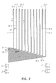
- FIG. 2 is a schematic top view illustrating a portion of the lead line structure depicted in FIG. 1 .
- FIG. 3A is a schematic cross-sectional view taken along a sectional line I-I′ depicted in FIG. 2 .
- FIG. 3B is a schematic cross-sectional view taken along a sectional line II-II′ depicted in FIG. 2 .
- FIG. 4 is a schematic cross-sectional view illustrating a lead line structure according to another embodiment of the invention.
- FIG. 5 is a schematic top view illustrating a portion of a lead line structure according to another embodiment of the invention.
- FIG. 6 is a schematic cross-sectional view taken along a sectional line depicted in FIG. 5 .
- FIG. 7 is a schematic cross-sectional view illustrating a lead line structure according to another embodiment of the invention.
- FIG. 8 is a schematic cross-sectional view illustrating a lead line structure according to another embodiment of the invention.
- FIG. 9 is a schematic cross-sectional view illustrating a lead line structure according to another embodiment of the invention.
- FIG. 10 is a schematic top view illustrating a display panel according to another embodiment of the invention.
- FIG. 1 is a schematic top view illustrating a display panel according to an embodiment of the invention.
- FIG. 2 is a schematic top view illustrating a portion of the lead line structure depicted in FIG. 1 .
- FIG. 3A is a schematic cross-sectional view taken along a sectional line I-I′ depicted in FIG. 2 .
- FIG. 3B is a schematic cross-sectional view taken along a sectional line II-IF depicted in FIG. 2 .
- the display panel of this embodiment includes a display region A and a non-display region B around the display region A.
- the display panel includes a pixel array AR, at least one driving device DR, a plurality of first lead lines L 1 - 1 ⁇ L 1 -n, a first insulating layer 102 , a plurality of second lead lines L 2 - 1 ⁇ L 2 -n, and a second insulating layer 106 .
- the pixel array AR is located in the display region A.
- the pixel array AR includes a plurality of scan lines SL 1 ⁇ SLn, a plurality of data lines DL 1 ⁇ DLn, and a plurality of pixel structures P.
- the scan lines SL 1 ⁇ SLn and the data lines DL 1 ⁇ DLn are alternately arranged, and an insulating layer is sandwiched between the scan lines SL 1 ⁇ SLn and the data lines DL 1 ⁇ DLn.
- extension directions of the data lines DL 1 ⁇ DLn are not parallel to extension directions of the scan lines SL 1 ⁇ SLn.
- the data lines DL 1 ⁇ DLn and the scan lines SL 1 ⁇ SLn are often made of metal materials. However, the invention is not limited thereto.
- the scan lines SL 1 ⁇ SLn and the data lines DL 1 ⁇ DLn can also be made of other conductive materials.
- the scan lines SL 1 ⁇ SLn and the data lines DL 1 ⁇ DLn can be made of an alloy, metal nitride, metal oxide, metal oxynitride, another appropriate material, or a layer in which a metal material and any other conductive material are stacked together.
- Each of the pixel structures P includes an active device T and a pixel electrode PE.
- the active device T can be a bottom-gate thin film transistor (TFT) or a top-gate TFT, and the active device T includes a gate, a channel, a source, and a drain.
- the active device T is electrically connected to a corresponding one of the scan lines SL 1 ⁇ SLn and a corresponding one of the data lines DL 1 ⁇ DLn.
- the active device T is electrically connected to the pixel electrode PE.
- the driving device DR is located in the non-display region B.
- the driving device DR can provide the pixel array AR with specific driving signals, so as to control the pixel array AR to display certain images.
- the driving device DR is disposed at one side of the display region A, which should not be construed as a limitation to the invention. According to other embodiments of the invention, the driving device can also be disposed at two sides of the display region A or disposed at the periphery of the display region A.
- the first lead lines L 1 - 1 ⁇ L 1 -n and the second lead lines L 2 - 1 ⁇ L 2 -n are located in the non-display region B and electrically connected to the pixel array AR and the driving device DR.
- the first lead lines L 1 - 1 ⁇ L 1 -n and the second lead lines L 2 - 1 ⁇ L 2 -n are electrically connected to the corresponding scan lines SL 1 ⁇ SLn and the corresponding data lines DL 1 ⁇ DLn, respectively.
- the driving signals of the driving device DR can be transmitted to the pixel array AR through the first lead lines L 1 - 1 ⁇ L 1 -n and the second lead lines L 2 - 1 ⁇ L 2 -n.
- first lead lines L 1 - 1 ⁇ L 1 -n and the second lead lines L 2 - 1 ⁇ L 2 -n are alternately arranged, i.e., the first lead lines L 1 - 1 ⁇ L 1 -n and the second lead lines L 2 - 1 ⁇ L 2 -n are arranged in the following order from left to right: the first lead line L 1 - 1 , the second lead line L 2 - 1 , the first lead line L 1 - 2 , the second lead line L 2 - 2 , . . . , the first lead line L 1 -n, and the second lead line L 2 -n.
- first lead lines L 1 - 1 ⁇ L 1 -n and the second lead lines L 2 - 1 ⁇ L 2 -n are often made of metal materials.
- first lead lines L 1 - 1 ⁇ L 1 -n and the second lead lines L 2 - 1 ⁇ L 2 -n can also be made of other conductive materials in other embodiments, which should not be construed as a limitation to the invention.
- the first lead lines L 1 - 1 ⁇ L 1 -n and the second lead lines L 2 - 1 ⁇ L 2 -n can be made of an alloy, metal nitride, metal oxide, metal oxynitride, another appropriate material, or a layer in which a metal material and any other conductive material are stacked together.
- the line width of each of the first lead lines L 1 - 1 ⁇ L 1 -n and the second lead lines L 2 - 1 ⁇ L 2 -n is approximately 3 ⁇ m ⁇ 6 ⁇ m, respectively. Based on the actual design requirements, the line width of each of the first lead lines L 1 - 1 ⁇ L 1 -n can be substantially the same as or different from the line width of each of the second lead lines L 2 - 1 ⁇ L 2 -n.
- the first lead lines L 1 - 1 ⁇ L 1 -n of this embodiment include first straight portions S 1 - 1 ⁇ S 1 -n and first oblique portions O 1 - 1 ⁇ O 1 -n connected to the first straight portions S 1 - 1 ⁇ S 1 -n.
- the first lead line L 1 - 1 includes the first straight portion S 1 - 1 and the first oblique portion O 1 - 1
- the first lead line L 1 - 2 includes the first straight portion S 1 - 2 and the first oblique portion O 1 - 2
- the first lead line L 1 -n includes the first straight portion S 1 -n and the first oblique portion O 1 -n.
- Extension directions of the first straight portions S 1 - 1 ⁇ S 1 -n are not parallel to extension directions of the first oblique portions O 1 - 1 ⁇ O 1 -n.
- the included angles between the extension directions of the first straight portions S 1 - 1 ⁇ S 1 -n and the extension directions of the first oblique portions O 1 - 1 ⁇ O 1 -n are not 0 degree or 180 degrees.
- the line width of each of the first straight portions S 1 - 1 ⁇ S 1 -n is substantially the same as the line width of each of the first oblique portions O 1 - 1 ⁇ O 1 -n, which should not be construed as a limitation to the invention.
- the second lead lines L 2 - 1 ⁇ L 2 -n of this embodiment include second straight portions S 2 - 1 ⁇ S 2 -n and second oblique portions O 2 - 1 ⁇ O 2 -n connected to the second straight portions S 2 - 1 ⁇ S 2 -n.
- the second lead line L 2 - 1 includes the second straight portion 52 - 1 and the second oblique portion O 2 - 1
- the second lead line L 2 - 2 includes the second straight portion S 2 - 2 and the second oblique portion O 2 - 2
- the second lead line L 2 -n includes the second straight portion S 2 -n and the second oblique portion O 2 -n.
- Extension directions of the second straight portions S 2 - 1 ⁇ S 2 -n are not parallel to extension directions of the second oblique portions O 2 - 1 ⁇ O 2 -n.
- the included angles between the extension directions of the second straight portions S 2 - 1 ⁇ S 2 -n and the extension directions of the second oblique portions O 2 - 1 ⁇ O 2 -n are not 0 degree or 180 degrees.
- the line width of each of the second straight portions S 2 - 1 ⁇ S 2 -n is substantially the same as the line width of each of the second oblique portions O 2 - 1 ⁇ O 2 -n, which should not be construed as a limitation to the invention.
- the first straight portions S 1 - 1 ⁇ S 1 -n of the first lead lines L 1 - 1 ⁇ L 1 -n are parallel to the second straight portions S 2 - 1 ⁇ S 2 -n of the second lead lines L 2 - 1 ⁇ L 2 -n, and the first straight portions S 1 - 1 ⁇ S 1 -n of the first lead lines L 1 - 1 ⁇ L 1 -n and the second straight portions S 2 - 1 ⁇ S 2 -n of the second lead lines L 2 - 1 ⁇ L 2 -n are extended toward and electrically connected to the driving device DR.
- the first oblique portions O 1 - 1 ⁇ O 1 -n of the first lead lines L 1 - 1 ⁇ L 1 -n are parallel to the second oblique portions O 2 - 1 ⁇ O 2 -n of the second lead lines L 2 - 1 ⁇ L 2 -n, and the first oblique portions O 1 - 1 ⁇ O 1 -n of the first lead lines L 1 -n and the second oblique portions O 2 - 1 ⁇ O 2 -n of the second lead lines L 2 - 1 ⁇ L 2 -n are extended toward and electrically connected to the pixel array AR.
- first distance D 1 there is a first distance D 1 between each of the first straight portions S 1 - 1 ⁇ S 1 -n of the first lead lines L 1 - 1 ⁇ L 1 -n and the adjacent one of the second straight portions S 2 - 1 ⁇ S 2 -n of the second lead lines L 2 - 1 ⁇ L 2 -n.
- the distance D 1 exists between the first straight portion S 1 - 1 and the second straight portion S 2 - 1 .
- the distance D 2 there is a second distance D 2 between each of the first oblique portions O 1 - 1 ⁇ O 1 -n of the first lead lines L 1 - 1 ⁇ L 1 -n and the adjacent one of the second oblique portions O 2 - 1 ⁇ O 2 -n of the second lead lines L 2 - 1 ⁇ L 2 -n.
- the distance D 2 exists between the first oblique portion O 1 - 1 and the second oblique portion O 2 - 1 .
- the first distance D 1 is substantially greater than the second distance D 2 .
- the first distance D 1 is approximately 10 ⁇ m ⁇ 20 ⁇ m
- the second distance D 2 is approximately 1.5 ⁇ m ⁇ 6 ⁇ m.
- the arrangement of the first straight portions S 1 - 1 ⁇ S 1 -n of the first lead lines L 1 - 1 ⁇ L 1 -n and the second straight portions S 2 - 1 ⁇ S 2 -n of the second lead lines L 2 - 1 ⁇ L 2 -n are not as dense as the arrangement of the first oblique portions O 1 - 1 ⁇ O 1 -n of the first lead lines L 1 - 1 ⁇ L 1 -n and the second oblique portions O 2 - 1 ⁇ O 2 -n of the second lead lines L 2 - 1 ⁇ L 2 -n.
- the first lead lines L 1 - 1 ⁇ L 1 -n are located on the substrate 100 , and the first insulating layer 102 covers the first lead lines L 1 - 1 ⁇ L 1 -n.
- the first insulating layer 102 can be made of an inorganic material (e.g., silicon oxide, silicon nitride, silicon oxynitride, any other suitable material, or a stacked layer containing at least two of the above materials), an organic material, any other suitable material, or a combination of the above.
- the first insulating layer 102 has a plurality of trenches 104 therein. In this embodiment, bottoms of the trenches 104 expose the substrate 100 . However, the invention is not limited thereto. The trenches 104 in other embodiments of the invention may not penetrate the first insulating layer 102 .
- the second lead lines L 2 - 1 ⁇ L 2 -n are respectively disposed in the trenches 104 of the first insulating layer 102 . Given the bottoms of the trenches 104 expose the substrate 100 , the second lead lines L 2 - 1 ⁇ L 2 -n are in direct contact with the surface of the substrate 100 . By contrast, given the trenches 104 do not penetrate the first insulating layer 102 , the second lead lines L 2 - 1 ⁇ L 2 -n are in contact with the first insulating layer 102 in the trenches 104 .
- the second insulating layer 106 covers the first insulating layer 102 and the second lead lines L 2 - 1 ⁇ L 2 -n.
- the second insulating layer 106 can be made of an inorganic material (e.g., silicon oxide, silicon nitride, silicon oxynitride, any other suitable material, or a stacked layer containing at least two of the above materials), an organic material, any other suitable material, or a combination of the above.
- the first lead lines L 1 - 1 ⁇ L 1 -n are covered and protected by the first and second insulating layers 102 and 106 , while the second lead lines L 2 - 1 ⁇ L 2 -n are covered by the second insulating layer 106 . Since the second lead lines L 2 - 1 ⁇ L 2 -n are disposed in the trenches 104 of the first insulating layer 102 , the height H 2 of the second insulating layer 106 above the second lead lines L 2 - 1 ⁇ L 2 -n is substantially smaller than the height H 1 of the second insulating layer 106 above the first lead lines L 1 - 1 ⁇ L 1 -n.
- the second lead lines L 2 - 1 ⁇ L 2 -n cannot be covered by two insulating layers, the second lead lines L 2 - 1 ⁇ L 2 -n are not apt to be directly damaged by external forces. This is because the height H 2 of the second insulating layer 106 above the second lead lines L 2 - 1 ⁇ L 2 -n is substantially smaller than the height H 1 of the second insulating layer 106 above the first lead lines L 1 - 1 ⁇ L 1 -n.
- the second insulating layer 106 above the first lead lines L 1 - 1 ⁇ L 1 -n is affected at first, and thereby the second lead lines L 2 - 1 ⁇ L 2 -n are less likely to be damaged directly by external forces.
- the second distance D 2 of this embodiment is relatively short, and thus the second straight portions S 2 - 1 ⁇ S 2 -n of the second lead lines L 2 - 1 ⁇ L 2 -n are disposed in the trenches 104 according to this embodiment, so as to prevent short circuit between the first oblique portions O 1 - 1 ⁇ O 1 -n of the first lead lines L 1 - 1 ⁇ L 1 -n and the adjacent second oblique portions O 2 - 1 ⁇ O 2 -n of the second lead lines L 2 - 1 ⁇ L 2 -n.
- the trenches 104 of the first insulating layer 102 are formed corresponding to the second straight portions S 2 - 1 ⁇ S 2 -n of the second lead lines L 2 - 1 ⁇ L 2 -n, as shown in FIG. 3A .
- the second oblique portions O 2 - 1 ⁇ O 2 -n of the second lead lines L 2 - 1 ⁇ L 2 -n are disposed on the surface of the first insulating layer 102 , as indicated in FIG. 3B .
- the second distance D 2 between each of the first oblique portions O 1 - 1 ⁇ O 1 -n of the first lead lines L 1 - 1 ⁇ L 1 -n and the adjacent one of the second oblique portions O 2 - 1 ⁇ O 2 -n of the second lead lines L 2 - 1 ⁇ L 2 -n is sufficient, and short circuit does not occur between the first oblique portions O 1 - 1 ⁇ O 1 -n and the adjacent second oblique portions O 2 - 1 ⁇ O 2 -n
- the second straight portions S 2 - 1 ⁇ S 2 -n and the second oblique portions O 2 - 1 ⁇ O 2 -n of the second lead lines L 2 - 1 ⁇ L 2 -n can all be disposed in the trenches 104 . That is to say, the trenches 104 of the first insulating layer 102 are formed corresponding to the second lead lines L 2 - 1 ⁇ L 2 -n
- FIG. 4 is a schematic cross-sectional view illustrating a lead line structure according to another embodiment of the invention.
- the lead line structure shown in FIG. 4 is similar to that shown in FIG. 3A , and thus same components in FIG. 4 and FIG. 3A are represented by the same numerals and not repeated herein.
- the lead line structure further includes a cover layer 108 that is disposed on the second insulating layer 106 above the second lead lines L 2 - 1 ⁇ L 2 -n.
- the cover layer 108 can be made of a metal material, a metal oxide material, an insulating material, or any other appropriate material.
- the second straight portions S 2 - 1 ⁇ S 2 -n of the second lead lines L 2 - 1 ⁇ L 2 -n are disposed in the trenches 104 , and the cover layer 108 is disposed on the second insulating layer 106 above the second straight portions S 2 - 1 S 2 -n of the second lead lines L 2 - 1 ⁇ L 2 -n, for instance.
- the invention is not limited thereto.
- the cover layer 108 can be correspondingly disposed on the second insulating layer 106 above the second straight portions S 2 - 1 ⁇ S 2 -n and the second oblique portions O 2 - 1 ⁇ O 2 -n of the second lead lines L 2 - 1 ⁇ L 2 -n.
- FIG. 5 is a schematic top view illustrating a portion of a lead line structure according to another embodiment of the invention.
- FIG. 6 is a schematic cross-sectional view taken along a sectional line depicted in FIG. 5 .
- the lead line structure of this embodiment is similar to the lead line structure shown in FIG. 2 , and thus the same components in these drawings are denoted by the same numerals and are not reiterated herein.
- the lead line structure further includes a plurality of protection structures 200 located between the second lead lines L 2 - 1 ⁇ L 2 -n and the adjacent first lead lines L 1 - 1 ⁇ L 1 -n.
- the protection structure 200 is disposed between the second lead line L 2 - 1 and the first lead line L 1 - 1 and between the second lead line L 2 - 1 and the first lead line L 1 - 2 .
- each protection structure 200 is substantially greater than the height H 2 of the second insulating layer 106 above the second lead lines L 2 - 1 ⁇ L 2 -n.
- the protection structures 200 are constituted by stacking a plurality of film layers.
- the film layers can be made of metal materials, insulating materials, semiconductor materials, metal oxide materials, and so forth, which is mainly determined based on the manufacturing process of the pixel array AR of the display panel and the material of the pixel array AR.
- each of the protection structures 200 of this embodiment is constituted by stacking a conductive pattern M 1 , the first insulating layer 102 , and the second insulating layer 106 .
- the conductive pattern M 1 is made of a metal material, for instance, and the metal material can be the same as the material of the first lead lines L 1 - 1 ⁇ L 1 -n.
- each protection structure 200 is constituted by stacking the conductive pattern M 1 , the first insulating layer 102 , and the second insulating layer 106 , and the second lead lines L 2 - 1 ⁇ L 2 -n are merely covered by the second insulating layer 106 . Accordingly, the height H 3 of each protection structure 200 is substantially greater than the height H 2 of the second insulating layer 106 above the second lead lines L 2 - 1 ⁇ L 2 -n. As such, when external forces are applied to the lead line structure, the protection structures 200 are firstly affected by the external forces, so as to prevent the second lead lines L 2 - 1 ⁇ L 2 -n from being damaged.
- each protection structure 200 is made of an insulating material, short circuit of the lead lines at respective sides of each protection structure 200 can be prevented.
- the invention is not limited thereto. If the distance between each protection structure 200 and the lead lines at the respective sides of the protection structure 200 is sufficient, the uppermost layer of the protection structure 200 is not required to be made of the insulating material.
- the protection structures 200 are disposed between the second straight portions S 2 - 1 ⁇ S 2 -n of the second lead lines L 2 - 1 ⁇ L 2 -n and the first straight portions S 1 - 1 ⁇ S 1 -n of the adjacent the first lead lines L 1 - 1 ⁇ L 1 -n.
- the protection structure 200 is disposed between the second straight portion S 2 - 1 of the second lead line L 2 - 1 and the first straight portion S 1 - 1 of the first lead line L 1 - 1 and between the second straight portion S 2 - 1 of the second lead line L 2 - 1 and the first straight portion S 1 - 2 of the first lead line L 1 - 2 .
- the height of each protection structure 200 is greater than the height of each of the second straight portions S 2 - 1 ⁇ S 2 -n of the second lead lines L 2 - 1 ⁇ L 2 -n.
- the invention is not limited thereto.
- the protection structures 200 can be further disposed between the second oblique portions O 2 - 1 ⁇ O 2 -n of the second lead lines L 2 - 1 ⁇ L 2 -n and the first oblique portions O 1 - 1 ⁇ O 1 -n of the adjacent first lead lines L 1 - 1 ⁇ L 1 -n.
- FIG. 7 is a schematic cross-sectional view illustrating a lead line structure according to another embodiment of the invention.
- the lead line structure of this embodiment is similar to the lead line structure shown in FIG. 6 , and thus the same components in these drawings are denoted by the same numerals and are not reiterated herein.
- each of the protection structures 200 of this embodiment is constituted by stacking the first insulating layer 102 , a conductive pattern M 2 , and the second insulating layer 106 .
- the conductive pattern M 2 is made of a metal material, for instance, and the metal material herein can be the same as the material of the second lead lines L 2 - 1 ⁇ L 2 -n.
- each protection structure 200 is constituted by stacking the first insulating layer 102 , the conductive pattern M 2 , and the second insulating layer 106 , and the second lead lines L 2 - 1 ⁇ L 2 -n are merely covered by the second insulating layer 106 , the height H 3 of each protection structure 200 is substantially greater than the height H 2 of the second insulating layer 106 above the second lead lines L 2 - 1 ⁇ L 2 -n.
- the protection structures 200 are firstly affected by the external forces, so as to prevent the second lead lines L 2 - 1 ⁇ L 2 -n from being damaged.
- FIG. 8 is a schematic cross-sectional view illustrating a lead line structure according to another embodiment of the invention.
- the lead line structure of this embodiment is similar to the lead line structure shown in FIG. 6 , and thus the same components in these drawings are denoted by the same numerals and are not reiterated herein.
- each of the protection structures 200 of this embodiment is constituted by stacking the conductive pattern M 1 , the first insulating layer 102 , an intermediate layer 202 , the conductive pattern M 2 , and the second insulating layer 106 .
- the conductive pattern M 1 is made of a metal material, for instance, and the metal material herein can be the same as the material of the first lead lines L 1 - 1 ⁇ L 1 -n.
- the intermediate layer 202 is made of a semiconductor material, for instance, and the semiconductor material can be amorphous silicon, polysilicon, micro-silicon, or a doped silicon material.
- the conductive pattern M 2 is made of a metal material, and the metal material herein can be the same as the material of the second lead lines L 2 - 1 ⁇ L 2 -n.
- each protection structure 200 is constituted by stacking the conductive pattern M 1 , the first insulating layer 102 , the intermediate layer 202 , the conductive pattern M 2 , and the second insulating layer 106 , and the second lead lines L 2 - 1 ⁇ L 2 -n are merely covered by the second insulating layer 106 , the height H 3 of each protection structure 200 is apparently greater than the height H 2 of the second insulating layer 106 above the second lead lines L 2 - 1 ⁇ L 2 -n.
- the protection structures 200 are firstly affected by the external forces, so as to prevent the second lead lines L 2 - 1 ⁇ L 2 -n from being damaged.
- FIG. 9 is a schematic cross-sectional view illustrating a lead line structure according to another embodiment of the invention.
- the lead line structure of this embodiment is similar to the lead line structure shown in FIG. 6 , and thus the same components in these drawings are denoted by the same numerals and are not reiterated herein.
- each of the protection structures 200 of this embodiment is constituted by stacking the conductive pattern M 1 , the first insulating layer 102 , the intermediate layer 202 , the conductive pattern M 2 , the second insulating layer 106 , and a cover layer 204 .
- the conductive pattern M 1 is made of a metal material, for instance, and the metal material herein can be the same as the material of the first lead lines L 1 - 1 ⁇ L 1 -n.
- the intermediate layer 202 is made of a semiconductor material, for instance, and the semiconductor material can be amorphous silicon, polysilicon, micro-silicon, or a doped silicon material.
- the conductive pattern M 2 is made of a metal material, and the metal material herein can be the same as the material of the second lead lines L 2 - 1 ⁇ L 2 -n.
- the cover layer 204 is made of a metal oxide material or an insulating material, for instance.
- each protection structure 200 is constituted by stacking the conductive pattern M 1 , the first insulating layer 102 , the intermediate layer 202 , the conductive pattern M 2 , the second insulating layer 106 , and the cover layer 204 , and the second lead lines L 2 - 1 ⁇ L 2 -n are merely covered by the second insulating layer 106 , the height H 3 of each protection structure 200 is apparently greater than the height H 2 of the second insulating layer 106 above the second lead lines L 2 - 1 ⁇ L 2 -n.
- the protection structures 200 are firstly affected by the external forces, so as to prevent the second lead lines L 2 - 1 ⁇ L 2 -n from being damaged.
- the driving device DR is disposed at a side of the display region A, and the scan lines SL 1 ⁇ SLn and the data lines DL 1 ⁇ DLn are electrically connected to the driving device DR.
- the driving devices are disposed at two sides of the display region A, and the scan lines SL 1 ⁇ SLn and the data lines DL 1 ⁇ DLn are electrically connected to the corresponding driving devices, respectively.
- FIG. 10 is a schematic top view illustrating a display panel according to another embodiment of the invention. This embodiment is similar to the embodiment shown in FIG. 1 , and thus the same components in these drawings are denoted by the same numerals and are not reiterated herein.
- the driving devices DR 1 and DR 2 of this embodiment are located in the non-display region B at two respective sides of the display region A, and the driving devices DR 1 and DR 2 can provide the pixel array AR with specific driving signals, so as to control the driving devices DR 1 and DR 2 to display certain images.
- the first lead lines L 1 - 1 ⁇ L 1 -n and the second lead lines L 2 - 1 ⁇ L 2 -n are located in the non-display region B and electrically connected to the pixel array AR and the driving devices DR 1 and DR 2 .
- the driving signals of the driving devices DR 1 and DR 2 can be transmitted to the pixel array AR through the first lead lines L 1 - 1 ⁇ L 1 -n and the second lead lines L 2 - 1 ⁇ L 2 -n.
- first lead lines L 1 - 1 ⁇ L 1 -n and the second lead lines L 2 - 1 ⁇ L 2 -n are alternately arranged, i.e., the first lead lines L 1 - 1 ⁇ L 1 -n and the second lead lines L 2 - 1 ⁇ L 2 -n are arranged in the following order from left to right: the first lead line L 1 - 1 , the second lead line L 2 - 1 , the first lead line L 1 - 2 , the second lead line L 2 - 2 , . . . , the first lead line L 1 -n, and the second lead line L 2 -n.
- the lead line structure (including the first lead lines L 1 - 1 ⁇ L 1 -n and the second lead lines L 2 - 1 ⁇ L 2 -n) in the display panel depicted in FIG. 10 can be the lead line structure described in any embodiment shown in FIG. 2 to FIG. 9 .
- the second lead lines are located in the trenches of the first insulating layer, and thereby the height of the second insulating layer above the second lead lines is substantially smaller than the height of the second insulating layer above the first lead lines. That is to say, unlike the first lead lines, the second lead lines cannot be covered by the first and second insulating layers. However, since the height of the second insulating layer above the second lead lines is substantially smaller than the height of the second insulating layer above the first lead lines, the second lead lines are less likely to be damaged.
- the protection structures can further protect the second lead lines from being damaged by external forces.
Landscapes
- Physics & Mathematics (AREA)
- Nonlinear Science (AREA)
- Mathematical Physics (AREA)
- Chemical & Material Sciences (AREA)
- Crystallography & Structural Chemistry (AREA)
- General Physics & Mathematics (AREA)
- Optics & Photonics (AREA)
- Electroluminescent Light Sources (AREA)
- Devices For Indicating Variable Information By Combining Individual Elements (AREA)
Abstract
Description
Claims (22)
Applications Claiming Priority (3)
| Application Number | Priority Date | Filing Date | Title |
|---|---|---|---|
| TW100115771A | 2011-05-05 | ||
| TW100115771 | 2011-05-05 | ||
| TW100115771A TWI516851B (en) | 2011-05-05 | 2011-05-05 | Lead line structure of liquid crystal display panel and liquid crystal display panel having the same |
Publications (2)
| Publication Number | Publication Date |
|---|---|
| US20120281369A1 US20120281369A1 (en) | 2012-11-08 |
| US8942000B2 true US8942000B2 (en) | 2015-01-27 |
Family
ID=44961544
Family Applications (1)
| Application Number | Title | Priority Date | Filing Date |
|---|---|---|---|
| US13/208,359 Active 2033-03-30 US8942000B2 (en) | 2011-05-05 | 2011-08-12 | Lead line structure and display panel having the same |
Country Status (3)
| Country | Link |
|---|---|
| US (1) | US8942000B2 (en) |
| CN (1) | CN102243403B (en) |
| TW (1) | TWI516851B (en) |
Families Citing this family (13)
| Publication number | Priority date | Publication date | Assignee | Title |
|---|---|---|---|---|
| CN103293727B (en) * | 2012-06-29 | 2016-02-17 | 上海中航光电子有限公司 | The array base palte of liquid crystal indicator |
| CN102799005A (en) * | 2012-09-07 | 2012-11-28 | 深圳市华星光电技术有限公司 | Design of fanout trace in TFT-LCD (thin film transistor-liquid crystal display) narrow frame design |
| KR102045244B1 (en) * | 2012-11-14 | 2019-11-15 | 엘지디스플레이 주식회사 | Flexible display device |
| US9614021B2 (en) * | 2013-07-24 | 2017-04-04 | Samsung Display Co., Ltd. | Organic light-emitting display apparatus and manufacturing method thereof |
| CN103874322B (en) * | 2014-02-28 | 2017-01-18 | 上海和辉光电有限公司 | Metal wire layout structure on insulation layer and preparation method thereof |
| JP6469427B2 (en) * | 2014-12-03 | 2019-02-13 | 株式会社ジャパンディスプレイ | Display device |
| CN107340623B (en) * | 2015-04-01 | 2020-05-22 | 上海天马微电子有限公司 | Array substrate, display panel and display device |
| CN106653722B (en) * | 2016-12-12 | 2019-09-24 | 厦门天马微电子有限公司 | Display panel and display device |
| CN108064403A (en) * | 2016-12-30 | 2018-05-22 | 深圳市柔宇科技有限公司 | Flexible display panels |
| CN107658285A (en) * | 2017-10-26 | 2018-02-02 | 惠科股份有限公司 | Fan-out line structure and manufacturing method thereof |
| CN108376685B (en) * | 2018-02-11 | 2021-02-09 | 上海天马微电子有限公司 | Display panels and display devices |
| JP6707156B2 (en) * | 2019-01-16 | 2020-06-10 | 株式会社ジャパンディスプレイ | Display device |
| KR102814639B1 (en) * | 2019-07-03 | 2025-05-29 | 삼성디스플레이 주식회사 | Display device |
Citations (10)
| Publication number | Priority date | Publication date | Assignee | Title |
|---|---|---|---|---|
| US5757450A (en) | 1994-09-08 | 1998-05-26 | Hitachi, Ltd. | Liquid crystal display with color filters and sizes of inclined linear wiring and terminal electrodes adjusted for equal resistances |
| JP2001305569A (en) | 2000-04-21 | 2001-10-31 | Hitachi Ltd | Liquid crystal display |
| JP2007079357A (en) | 2005-09-16 | 2007-03-29 | Sanyo Epson Imaging Devices Corp | Display apparatus |
| JP2007094028A (en) | 2005-09-29 | 2007-04-12 | Sanyo Epson Imaging Devices Corp | Liquid crystal display device |
| US7956978B2 (en) * | 1995-12-21 | 2011-06-07 | Semiconductor Energy Laboratory Co., Ltd. | Liquid-crystal display device having a particular conductive layer |
| US8259276B2 (en) * | 2008-11-12 | 2012-09-04 | Au Optronics Corporation | Active device array substrate with plurality of marks in a peripheral area and liquid crystal display panel |
| US8355087B2 (en) * | 2010-08-19 | 2013-01-15 | Au Optronics Corporation | Pixel array substrate, conductive structure and display panel |
| US8405809B2 (en) * | 2011-04-13 | 2013-03-26 | Au Optronics Corporation | Lead line structure and display panel having the same |
| US20130235020A1 (en) * | 2012-03-06 | 2013-09-12 | Apple Inc. | Pixel inversion artifact reduction |
| US8643820B2 (en) * | 1996-06-25 | 2014-02-04 | Semiconductor Energy Laboratory Co., Ltd. | Electronic device having liquid crystal display device |
Family Cites Families (4)
| Publication number | Priority date | Publication date | Assignee | Title |
|---|---|---|---|---|
| KR20020083249A (en) * | 2001-04-26 | 2002-11-02 | 삼성전자 주식회사 | A contact structure of a wires and method manufacturing the same, and thin film transistor substrate including the contact structure and method manufacturing the same |
| CN100477234C (en) * | 2005-09-27 | 2009-04-08 | 中华映管股份有限公司 | Thin film transistor array substrate |
| CN201378237Y (en) * | 2009-03-17 | 2010-01-06 | 华映光电股份有限公司 | Picture element array substrate |
| CN101697053B (en) * | 2009-09-23 | 2011-11-16 | 深超光电(深圳)有限公司 | Active component array substrate |
-
2011
- 2011-05-05 TW TW100115771A patent/TWI516851B/en active
- 2011-06-28 CN CN201110184699.8A patent/CN102243403B/en active Active
- 2011-08-12 US US13/208,359 patent/US8942000B2/en active Active
Patent Citations (10)
| Publication number | Priority date | Publication date | Assignee | Title |
|---|---|---|---|---|
| US5757450A (en) | 1994-09-08 | 1998-05-26 | Hitachi, Ltd. | Liquid crystal display with color filters and sizes of inclined linear wiring and terminal electrodes adjusted for equal resistances |
| US7956978B2 (en) * | 1995-12-21 | 2011-06-07 | Semiconductor Energy Laboratory Co., Ltd. | Liquid-crystal display device having a particular conductive layer |
| US8643820B2 (en) * | 1996-06-25 | 2014-02-04 | Semiconductor Energy Laboratory Co., Ltd. | Electronic device having liquid crystal display device |
| JP2001305569A (en) | 2000-04-21 | 2001-10-31 | Hitachi Ltd | Liquid crystal display |
| JP2007079357A (en) | 2005-09-16 | 2007-03-29 | Sanyo Epson Imaging Devices Corp | Display apparatus |
| JP2007094028A (en) | 2005-09-29 | 2007-04-12 | Sanyo Epson Imaging Devices Corp | Liquid crystal display device |
| US8259276B2 (en) * | 2008-11-12 | 2012-09-04 | Au Optronics Corporation | Active device array substrate with plurality of marks in a peripheral area and liquid crystal display panel |
| US8355087B2 (en) * | 2010-08-19 | 2013-01-15 | Au Optronics Corporation | Pixel array substrate, conductive structure and display panel |
| US8405809B2 (en) * | 2011-04-13 | 2013-03-26 | Au Optronics Corporation | Lead line structure and display panel having the same |
| US20130235020A1 (en) * | 2012-03-06 | 2013-09-12 | Apple Inc. | Pixel inversion artifact reduction |
Non-Patent Citations (1)
| Title |
|---|
| "Office Action of Taiwan Counterpart Application", issued on May 9, 2014, p. 1-p. 6, in which the listed references were cited. |
Also Published As
| Publication number | Publication date |
|---|---|
| US20120281369A1 (en) | 2012-11-08 |
| CN102243403B (en) | 2014-04-23 |
| TWI516851B (en) | 2016-01-11 |
| TW201245827A (en) | 2012-11-16 |
| CN102243403A (en) | 2011-11-16 |
Similar Documents
| Publication | Publication Date | Title |
|---|---|---|
| US11825713B2 (en) | Display device | |
| US20120281369A1 (en) | Lead line structure and display panel having the same | |
| US10707429B2 (en) | Flexible display panel and flexible display apparatus | |
| CN112786647B (en) | Display device having substrate hole | |
| US8405809B2 (en) | Lead line structure and display panel having the same | |
| KR20230169048A (en) | Flexible display device | |
| US10153322B2 (en) | Organic light emitting display device | |
| KR102111562B1 (en) | Thin film semiconductor device and organic light emitting display | |
| KR102557445B1 (en) | Display device | |
| US9922909B2 (en) | Display device | |
| US20180197924A1 (en) | Touch sensor and display device having touch sensor | |
| US20180061728A1 (en) | Display panel with dam structure | |
| CN106444119B (en) | Display device | |
| US9064749B2 (en) | Array substrate | |
| US20150021708A1 (en) | Pixel structure | |
| US8941804B2 (en) | Liquid crystal display device | |
| US10067393B2 (en) | Thin film display panel and liquid crystal display device including the same | |
| KR102172386B1 (en) | Thin film transistor array substrate and manufacturing method of the same | |
| US20120112199A1 (en) | Thin film transistor array panel | |
| TW202018992A (en) | Pixel structure | |
| US20150279865A1 (en) | Semiconductor device and display device | |
| US20160209690A1 (en) | Display device | |
| US20150255616A1 (en) | Semiconductor device and display device | |
| US9853058B2 (en) | Thin film transistor array panel and display device including the same | |
| JP2008180807A (en) | Electro-optical device, and electronic apparatus equipped with the same |
Legal Events
| Date | Code | Title | Description |
|---|---|---|---|
| AS | Assignment |
Owner name: AU OPTRONICS CORPORATION, TAIWAN Free format text: ASSIGNMENT OF ASSIGNORS INTEREST;ASSIGNORS:CHEN, CHIEN-LI;CHIANG, PEI-LING;LEE, WEI-HSIN;REEL/FRAME:026746/0874 Effective date: 20110803 |
|
| STCF | Information on status: patent grant |
Free format text: PATENTED CASE |
|
| MAFP | Maintenance fee payment |
Free format text: PAYMENT OF MAINTENANCE FEE, 4TH YEAR, LARGE ENTITY (ORIGINAL EVENT CODE: M1551) Year of fee payment: 4 |
|
| MAFP | Maintenance fee payment |
Free format text: PAYMENT OF MAINTENANCE FEE, 8TH YEAR, LARGE ENTITY (ORIGINAL EVENT CODE: M1552); ENTITY STATUS OF PATENT OWNER: LARGE ENTITY Year of fee payment: 8 |
|
| AS | Assignment |
Owner name: NEOLAYER LLC, TEXAS Free format text: ASSIGNMENT OF ASSIGNORS INTEREST;ASSIGNOR:AUO CORPORATION;REEL/FRAME:072266/0941 Effective date: 20250701 |
|
| MAFP | Maintenance fee payment |
Free format text: PAYMENT OF MAINTENANCE FEE, 12TH YEAR, LARGE ENTITY (ORIGINAL EVENT CODE: M1553); ENTITY STATUS OF PATENT OWNER: LARGE ENTITY Year of fee payment: 12 |