US8922186B2 - Method and apparatus for all duty current sensing in current mode converter - Google Patents
Method and apparatus for all duty current sensing in current mode converter Download PDFInfo
- Publication number
- US8922186B2 US8922186B2 US13/628,025 US201213628025A US8922186B2 US 8922186 B2 US8922186 B2 US 8922186B2 US 201213628025 A US201213628025 A US 201213628025A US 8922186 B2 US8922186 B2 US 8922186B2
- Authority
- US
- United States
- Prior art keywords
- current
- sensing
- bridge
- coupled
- module
- Prior art date
- Legal status (The legal status is an assumption and is not a legal conclusion. Google has not performed a legal analysis and makes no representation as to the accuracy of the status listed.)
- Active, expires
Links
- 238000000034 method Methods 0.000 title description 14
- 230000009466 transformation Effects 0.000 claims description 22
- 239000003990 capacitor Substances 0.000 claims description 15
- 230000001131 transforming effect Effects 0.000 claims description 5
- 230000003321 amplification Effects 0.000 claims description 4
- 238000003199 nucleic acid amplification method Methods 0.000 claims description 4
- 238000010586 diagram Methods 0.000 description 24
- 238000005259 measurement Methods 0.000 description 16
- 230000008569 process Effects 0.000 description 12
- 238000004088 simulation Methods 0.000 description 9
- 230000008859 change Effects 0.000 description 6
- 230000000737 periodic effect Effects 0.000 description 4
- 238000004364 calculation method Methods 0.000 description 2
- 230000004044 response Effects 0.000 description 2
- 230000003044 adaptive effect Effects 0.000 description 1
- 230000004075 alteration Effects 0.000 description 1
- 230000015556 catabolic process Effects 0.000 description 1
- 230000003247 decreasing effect Effects 0.000 description 1
- 238000006731 degradation reaction Methods 0.000 description 1
- 230000000694 effects Effects 0.000 description 1
- 238000012986 modification Methods 0.000 description 1
- 230000004048 modification Effects 0.000 description 1
Images


Classifications
-
- H—ELECTRICITY
- H02—GENERATION; CONVERSION OR DISTRIBUTION OF ELECTRIC POWER
- H02M—APPARATUS FOR CONVERSION BETWEEN AC AND AC, BETWEEN AC AND DC, OR BETWEEN DC AND DC, AND FOR USE WITH MAINS OR SIMILAR POWER SUPPLY SYSTEMS; CONVERSION OF DC OR AC INPUT POWER INTO SURGE OUTPUT POWER; CONTROL OR REGULATION THEREOF
- H02M3/00—Conversion of DC power input into DC power output
- H02M3/02—Conversion of DC power input into DC power output without intermediate conversion into AC
- H02M3/04—Conversion of DC power input into DC power output without intermediate conversion into AC by static converters
- H02M3/10—Conversion of DC power input into DC power output without intermediate conversion into AC by static converters using discharge tubes with control electrode or semiconductor devices with control electrode
- H02M3/145—Conversion of DC power input into DC power output without intermediate conversion into AC by static converters using discharge tubes with control electrode or semiconductor devices with control electrode using devices of a triode or transistor type requiring continuous application of a control signal
- H02M3/155—Conversion of DC power input into DC power output without intermediate conversion into AC by static converters using discharge tubes with control electrode or semiconductor devices with control electrode using devices of a triode or transistor type requiring continuous application of a control signal using semiconductor devices only
- H02M3/156—Conversion of DC power input into DC power output without intermediate conversion into AC by static converters using discharge tubes with control electrode or semiconductor devices with control electrode using devices of a triode or transistor type requiring continuous application of a control signal using semiconductor devices only with automatic control of output voltage or current, e.g. switching regulators
- H02M3/158—Conversion of DC power input into DC power output without intermediate conversion into AC by static converters using discharge tubes with control electrode or semiconductor devices with control electrode using devices of a triode or transistor type requiring continuous application of a control signal using semiconductor devices only with automatic control of output voltage or current, e.g. switching regulators including plural semiconductor devices as final control devices for a single load
- H02M3/1588—Conversion of DC power input into DC power output without intermediate conversion into AC by static converters using discharge tubes with control electrode or semiconductor devices with control electrode using devices of a triode or transistor type requiring continuous application of a control signal using semiconductor devices only with automatic control of output voltage or current, e.g. switching regulators including plural semiconductor devices as final control devices for a single load comprising at least one synchronous rectifier element
-
- H—ELECTRICITY
- H02—GENERATION; CONVERSION OR DISTRIBUTION OF ELECTRIC POWER
- H02M—APPARATUS FOR CONVERSION BETWEEN AC AND AC, BETWEEN AC AND DC, OR BETWEEN DC AND DC, AND FOR USE WITH MAINS OR SIMILAR POWER SUPPLY SYSTEMS; CONVERSION OF DC OR AC INPUT POWER INTO SURGE OUTPUT POWER; CONTROL OR REGULATION THEREOF
- H02M1/00—Details of apparatus for conversion
- H02M1/0003—Details of control, feedback or regulation circuits
- H02M1/0009—Devices or circuits for detecting current in a converter
-
- Y—GENERAL TAGGING OF NEW TECHNOLOGICAL DEVELOPMENTS; GENERAL TAGGING OF CROSS-SECTIONAL TECHNOLOGIES SPANNING OVER SEVERAL SECTIONS OF THE IPC; TECHNICAL SUBJECTS COVERED BY FORMER USPC CROSS-REFERENCE ART COLLECTIONS [XRACs] AND DIGESTS
- Y02—TECHNOLOGIES OR APPLICATIONS FOR MITIGATION OR ADAPTATION AGAINST CLIMATE CHANGE
- Y02B—CLIMATE CHANGE MITIGATION TECHNOLOGIES RELATED TO BUILDINGS, e.g. HOUSING, HOUSE APPLIANCES OR RELATED END-USER APPLICATIONS
- Y02B70/00—Technologies for an efficient end-user side electric power management and consumption
- Y02B70/10—Technologies improving the efficiency by using switched-mode power supplies [SMPS], i.e. efficient power electronics conversion e.g. power factor correction or reduction of losses in power supplies or efficient standby modes
Definitions
- the present invention relates to a current sensing apparatus and a voltage converter apparatus, and more particularly, to a current sensing apparatus and a voltage converter apparatus which can simultaneously measure conduction currents of an up-bridge circuit and a down-bridge circuit.
- FIG. 1 illustrates a conventional schematic diagram of a voltage converter 10 .
- the voltage converter 10 is utilized to transform an input voltage Vin into an output voltage Vout, and includes a controller 100 , a gate driver 101 , a driver circuit 102 , an output circuit 104 , a feedback circuit 106 , a current sensing module 108 , an error amplifier A_ERR and a pulse width modulation comparator A_PWM.
- the controller 100 is coupled to the gate driver 101 .
- the gate driver 101 includes an inverter Inv 1 , buffer amplifiers BA 1 , BA 2 , and is coupled to the driver circuit 102 and the current sensing circuit 108 .
- the driver circuit 102 includes switch transistors SW 1 , SW 2 , and is coupled to the output circuit 104 and the current sensing circuit 108 .
- the output circuit 104 includes an inductor L 1 and a capacitor C 1 , and is coupled to the feedback circuit 106 .
- the feedback circuit 106 includes resistors R 1 , R 2 and is coupled to the error amplifier A_ERR.
- the pulse width modulation comparator A_PWM is coupled to the current sensing circuit 108 and the controller 100 .
- the current sensing circuit 108 includes a current comparator A_CS, a current generator Cs, a capacitor C 2 , an inverter Inv 2 and switch elements S 1 , S 2 .
- the controller 100 utilizes a pulse width modulation signal or a reset signal Rst to generate a control signal to be transmitted to the gate driver 101 .
- the gate driver 101 utilizes the control signal to correspondingly switch on/off the switch transistors SW 1 , SW 2 . Accordingly, the input voltage Vin is transformed into the output voltage Vout via the switch transistors SW 1 , SW 2 and the output circuit 104 .
- the feedback circuit 106 utilizes the resistors R 1 , R 2 to transform the output voltage Vout into a feedback signal to be transmitted to the error amplifier A_ERR.
- the error amplifier A_ERR compares the feedback signal and a reference voltage Vref to output an error signal.
- the current sensing circuit 108 utilizes the current comparator A_CS to compare conduction currents passing through two points P 1 and P 2 of the switch transistor SW 2 , so as to generate a comparison signal.
- the current generator Cs utilizes a resistor (not shown in the figure) to transform a difference between the input voltage Vin and the output voltage Vout into a current source to be outputted.
- the control signal is utilized to switch on/off the switch elements S 1 , S 2 such that the comparison signal or the current source is utilized to charge the capacitor C 2 to generate a charging voltage value.
- the pulse width modulation comparator A_PWM compares a difference between the charging voltage value and the error signal to generate the pulse width modulation signal to be transmitted to the controller 100 .
- the voltage converter apparatus 10 simultaneously utilizes the reset signal Rst and the pulse width modulation signal to correspondingly change a duty cycle for driving the driver circuit 102 , so as to adaptively transform the input voltage Vin into the output voltage Vout to satisfy different users' requirements.
- inductance changes of the inductor L 1 may correspondingly change an inductor-current slope between an input stage and an output stage, so as to change values of the output voltage as well as the feedback signal.
- a circuit designer must predetermine values of the input voltage Vin and the output voltage Vout, so as to pre-store the above values inside the current comparator A_CS as the charging voltage value of the capacitor C 2 . Therefore, users are unable to utilize the current sensing circuit 108 to immediately respond to related conduction information of the voltage converter apparatus 10 , which may influence generation of the pulse width modulation signal to reduce efficiency or accuracy for transforming the input voltage Vin into the output voltage Vout.
- conduction periods of the switch transistor SW 1 and SW 2 may influence the generation of the pulse width modulation signal.
- a ratio of turning on the switch transistors SW 1 and SW 2 is 9:1, respectively. Since the conduction period of the switch transistor SW 2 is too short or a switch frequency of the switch transistor SW 2 is too high for the users to measure the conduction current passing through the switch transistor SW 2 .
- the users may have difficulties obtaining the related conduction information of the switch transistor SW 2 , such as a slope change of the conduction current passing through the switch transistor SW 2 . Accordingly, the product application of the voltage converter apparatus 10 will be limited.
- the present invention discloses a current sensing apparatus for a voltage converter apparatus comprising a circuit selection module coupled to a clock generator of the voltage converter apparatus and a controller for generating a circuit selection result according to a clock signal generated by the clock generator and a duty cycle signal generated by the controller, a current sensing module coupled to the circuit selection module, an up-bridge circuit and a down-bridge circuit for measuring an up-bridge conduction current of the up-bridge circuit or a down-bridge conduction current of the down-bridge circuit according to the circuit selection result, and a current generation module coupled to the current sensing module and a slope compensation circuit of the voltage converter apparatus for generating a sensing voltage according to a slope compensation current generated by the slope compensation circuit and the up-bridge conduction current or the down-bridge conduction current, so as to adjust the duty cycle signal of the controller, wherein the current sensing apparatus utilizes the duty cycle signal to drive the voltage converter apparatus.
- the present invention also discloses another voltage converter apparatus comprising an input terminal for receiving an input voltage, an output terminal for outputting an output voltage, a clock generator for generating a clock signal, a controller coupled to the clock generator for receiving the clock signal to generate an duty cycle signal, an inverter coupled to the controller for receiving the duty cycle signal to generate a reverse phase duty cycle signal, a gate driver coupled to the inverter for receiving the reverse phase duty cycle signal to generate a gate control signal, a driver circuit comprising an up-bridge circuit and a down-bridge circuit for receiving the gate control signal to control conduction conditions of the up-bridge circuit and the down-bridge circuit, an inductor comprising one end coupled to the driver circuit and another end coupled to the output terminal, a feedback module coupled to the output terminal for generating a feedback signal according to the output voltage, an error amplifier coupled to the feedback module for generating an amplification signal according to the feedback signal and a reference voltage, a loop compensation network coupled to the error amplifier for generating a compensation result according to the amplification signal, a slope
- FIG. 1 illustrates a conventional schematic diagram of a voltage converter.
- FIG. 2 illustrates a schematic diagram of a voltage converter according to an embodiment of the invention.
- FIG. 3 illustrates a schematic diagram of the circuit selection module generating the circuit selection result according to an embodiment of the invention.
- FIG. 4 illustrates a detailed schematic diagram of the current sensing module coupled to the current generation module according to an embodiment of the invention.
- FIG. 5 illustrates a detailed schematic diagram of a multiplier shown in FIG. 4 according to an embodiment of the invention.
- FIG. 6 illustrates a schematic diagram of a measurement result of the circuit sensing module according to an embodiment of the invention.
- FIG. 7A illustrates a schematic diagram of an output result of the current generation module according to an embodiment of the invention.
- FIG. 7B illustrates a schematic diagram of another output result of the current generation module according to an embodiment of the invention.
- FIG. 8A illustrates a schematic diagram of a practical measurement of the current sensing module according to an embodiment of the invention.
- FIG. 8B illustrates a schematic diagram of another practical measurement of the current sensing module according to an embodiment of the invention.
- FIG. 8C illustrates a schematic diagram of another practical measurement of the current sensing module according to an embodiment of the invention.
- FIG. 8D illustrates a schematic diagram of another practical measurement of the current sensing module according to an embodiment of the invention.
- FIG. 9 illustrates a flow chart of a current sensing process according to an embodiment of the invention.
- FIG. 10 illustrates a flow chart of a voltage transformation process according to an embodiment of the invention.
- FIG. 2 illustrates a schematic diagram of a voltage converter apparatus 20 according to an embodiment of the invention.
- the voltage converter apparatus 20 includes a controller 200 , a gate driver 201 , a driver circuit 202 , a clock generator 203 , an output circuit 204 , a feedback circuit 206 , a current sensing circuit 208 , an error amplifier 210 , a loop compensation network 212 , a pulse width modulation comparator 214 and a slope compensation circuit 216 .
- the voltage converter apparatus 20 is similar to the voltage converter apparatus 10 , and further includes the current sensing module 208 including a circuit selection module 2080 , a current sensing module 2082 and a current generation module 2084 to simultaneously measure conduction currents of an up-bridge circuit and a down-bridge circuit.
- the current sensing module 208 including a circuit selection module 2080 , a current sensing module 2082 and a current generation module 2084 to simultaneously measure conduction currents of an up-bridge circuit and a down-bridge circuit.
- the controller 200 is coupled to the gate driver 201 via an inverter Inv 3 . Also, the controller 200 is coupled to the clock generator 203 , the current sensing circuit 208 and the pulse width modulation comparator 214 .
- the driver circuit 202 includes switch transistors SWP, SWN to be realized via a P-type MOS transistor and an N-type MOS transistor.
- the switch transistor SWP is regarded as an up-bridge circuit and the switch transistor SWN is regarded as a down-bridge circuit, and the gate driver 201 is coupled to gates of the switch transistors SWP, SWN. Besides, one end of the switch transistor SWP receives an input voltage VIN, and one end of the switch transistor SWN is grounded.
- the other ends of the switch transistors SWP, SWN are both coupled to the output circuit 204 .
- the output circuit 204 includes an inductor L 1 and a capacitor COUT. One end of the inductor L 1 is coupled to the switch transistors SWP, SWN, and another end of the inductor L 1 is coupled to one end of the capacitor COUT, a feedback circuit 206 and an output terminal to output an output voltage VOUT.
- the feedback circuit 206 includes resistors R 3 , R 4 , wherein one end of the resistor R 3 is coupled to one end of the resistor R 4 and the error amplifier 210 , and another end of the resistor R 4 is grounded.
- the error amplifier 210 receives a reference voltage VREF and is coupled to one end of the loop compensation network 212 , and another end of the loop compensation network 212 is coupled to the pulse width modulation comparator 214 .
- the circuit selection module 2080 is coupled to the clock generator 203 and the current sensing module 2082 .
- the current sensing module 2082 includes an up-bridge measurement module 2082 _UP and a down-bridge measurement module 2082 _DN to be coupled to a terminal point P 3 of the switch transistor SWP and a terminal point P 4 of the switch transistor SWN, respectively.
- the current generation module 2084 is coupled to the current sensing module 2082 , the slope compensation circuit 216 and the pulse width modulation comparator 214 .
- the controller 200 receives a pulse width modulation signal S_PWM and a clock signal S_CLK to correspondingly output a duty cycle signal S_Duty.
- the inverter Inv 3 inverts the duty cycle signal S_Duty to S_RDuty, and the gate driver 201 receives an reverse duty cycle signal S_RDuty to correspondingly generate a gate control signal S_G.
- the switch transistors SWP, SWN are turned on/off via the gate control signal S_G, and the capacitor COUT and the inductor L 1 generate the frequency response to transform the input voltage VIN into the output voltage VOUT.
- the feedback circuit 206 utilizes a resistance ratio of the resistor R 3 and R 4 to transform the output voltage VOUT into a feedback signal S_FB to be transmitted to the error amplifier 210 .
- the error amplifier 210 compares the feedback signal S_FB and the reference voltage VREF to correspondingly output an error signal S_ERR.
- the error signal S_ERR passing through the loop compensation network 212 is transformed into a compensation result EAO to the pulse width modulation comparator 214 .
- the circuit selection module 2080 compares the clock signal S_CLK and the duty cycle signal S_Duty to generate a circuit selection result S_DCS.
- FIG. 3 illustrates a schematic diagram of the circuit selection module 2080 generating the circuit selection result S_DSC according to an embodiment of the invention.
- the clock signal S_CLK is transformed into a clock comparison signal TON_MIN via the circuit selection module 2080 and an up-edge driving process.
- the clock signal S_CLK and the clock comparison signal TON_MIN share the same periodic period, and each pulse of the clock signal S_CLK and the clock comparison signal TON_MIN have different pulse width.
- the duty cycle signal S_Duty is controlled by the controller 200 to adaptively change pulse duration. Through a comparator (not shown in the figure), if the single pulse duration of the duty cycle signal S_Duty is shorter than the single pulse duration of the clock comparison signal TON_MIN, the circuit selection result S_DCS is generated.
- the up-bridge sensing module 2082 _UP and the down-bridge sensing module 2082 _DN receive the circuit selection result S_DCS to determine how long up-bridge sensing module 2082 _UP or the down-bridge sensing module 2082 _DN measures the driver circuit 202 . For example, when the circuit selection result S_DCS equals 0 at a first period corresponding to the conduction period of the switch transistor SWP in the duty cycle signal S_Duty, the up-bridge sensing module 2082 _UP measures a up-bridge conduction current ISENP at the terminal point P 3 of the switch transistor SWP.
- the down-bridge sensing module 2082 _DN measures a down-bridge conduction current ISENN at the terminal point P 4 of the switch transistor SWN. Accordingly, an output element 2082 _O receives the up-bridge conduction current ISENP and the down-bridge conduction current ISENN to obtain the sensing current ⁇ I_SEN and a valley current value I_DN.
- the down-bridge sensing module 2082 _DN also receives the duty cycle signal S_Duty for determination of the following calculation. Noticeably, the embodiment of the invention mainly focuses on the conduction period of the switch transistor SWP (i.e.
- the user can adaptively modify/change the above embodiment according to different users' requirements, which is not limiting the scope of the invention.
- FIG. 4 illustrates a detailed schematic diagram of the current sensing module 2082 coupled to the current generation module 2084 according to an embodiment of the invention.
- a switch module 2082 _DNS receives the duty cycle signal S_Duty, wherein the switch module 2082 _DNS includes two transistors forming a conduction switch and is coupled to a filter 2082 _DNF including a resistor 2082 _DNR and a capacitor 2082 _DNC.
- the duty cycle signal S_Duty is transformed into a current clock signal via the switch module 2082 _DNS, and the filter 2082 _DNF is utilized to transform the current clock signal into an analogy duty cycle signal S_ADuty.
- FIG. 5 illustrates a detailed schematic diagram of a multiplier 400 shown in FIG. 4 according to an embodiment of the invention.
- the multiplier 400 receives the analogy duty cycle signal SADuty and twice current difference ⁇ I_S. Through a plurality of cascoded transistors and a current mirror effect, an adjusted current difference ⁇ I_AS is correspondingly outputted.
- a transformation module 402 is coupled to the multiplier 400 to receive the adjusted current difference ⁇ I_AS.
- the switch elements 4020 , 4026 of the transformation module 402 receive the reverse duty cycle signal S_RDuty, and a transformation unit 4022 and a sensing capacitor 4024 is utilized to transform the adjusted current difference ⁇ I_AS into an adjustment voltage difference ⁇ V_SEN.
- the adjustment voltage difference ⁇ V_SEN is utilized to process a charging operation for the sensing capacitor 4024
- the switch element 4026 is utilized to control a charging period of the sensing capacitor 4024 .
- a voltage-current converter 404 is utilized to receive the adjustment voltage difference ⁇ V_SEN to output a sensing current difference ⁇ I_SEN.
- an output module 406 is utilized to receive the ⁇ I_SEN and the valley current I_DN to correspondingly output a sensing result S_DNS.
- An adder 2084 _ADD of the current generation module 2084 receives the sensing result S_DNS and a slope compensation current S_ISL to generate a sensing current S_SI.
- a transformation resistor 2084 _R is utilized to transform the sensing current S_SI into a sensing voltage S_SV to be outputted to the pulse width modulation comparator 214 .
- the pulse width modulation comparator 214 compares the compensation result EAO and the sensing voltage S_SV to generate a pulse width modulation signal S_PWM to the controller 200 , so as to control the controller 200 to generate different duty cycle signals S_Duty.
- the voltage converter apparatus 20 adaptively transforms the input voltage VIN into the output voltage VOUT according to different duty cycle signals S_Duty to satisfy different users' requirements.
- FIG. 6 illustrates a schematic diagram of a measurement result of the circuit sensing module 2082 according to an embodiment of the invention, wherein the X-axis represents the timing and the Y-axis represents the current values, the symbol Ts represents a total periodic period, the symbol D represents the conduction period of the switch transistor SWP and the symbol 1 -D represents the conduction period of the switch transistor SWN.
- the down-bridge sensing module 2082 _DN measures the down-bridge conduction current ISENN at the timing T 1 to obtain information of a point H 1 .
- the down-bridge conduction current ISENN is measured at the timing T 2 to obtain information of a point H 2 . Accordingly, the current difference ⁇ I_S is obtained.
- the conduction period 1 -D and the current difference ⁇ I_S can be both utilized to derive a slope m 2 (i.e. the segment from the point H 1 to the point H 2 ), and the information from the point H 2 (i.e.
- the value of the down-bridge conduction valley current I_DN) to the point H 3 can be copied to derive a slope m 1 (i.e. the segment from the point H 3 to the point H 1 ), so as to reconstruct the segment/figure from the point H 3 via the point H 1 and to the point H 2 .
- the down-bridge sensing module 2082 _DN copies the current passing through the switch transistor SWN to be the current passing through the switch transistor SWP, so as to derive the conduction current passing through the switch transistor SWP.
- the circuit sensing module 208 can automatically select to measure the conduction currents of the switch transistor SWP or the switch transistor SWN, so as to obtain an average value I_OUT of the conduction currents.
- FIG. 7A illustrates a schematic diagram of an output result of the current generation module 2084 according to an embodiment of the invention, wherein the current generation module 2084 is predetermined a sensing resistor R_SEN, such as the transformation resistor 2084 _R, to pre-measure a zero-current conduction voltage V_ZCV.
- the valley current I_DN is multiplied by the sensing resistor R_SEN, and the multiplication is added with the zero-current conduction voltage V_ZCV to obtain a first voltage value V 1 .
- the current difference ⁇ I_S is added with the slope compensation current S_ISL, and the sum is multiplied by the sensing resistor R_SEN to be added with the first voltage value V 1 , so as to obtain a second voltage value V 2 .
- the second voltage value V 2 is the sensing voltage S_SV to be transmitted to the pulse width modulation comparator 214 for following operations, which have been explained in the above paragraphs without redundancy description hereinafter.
- FIG. 7B illustrates a schematic diagram of another output result of the current generation module 2084 according to an embodiment of the invention.
- the operation shown in FIG. 7B can be processed if the down-bridge sensing module 2082 _DN can accurately measure a peak current I_UP.
- the peak current I_UP is multiplied by the sensing resistor R_SEN to be added with the pre-measured zero-current conduction voltage V_ZCV, so as to obtain a third voltage value V 3 .
- the slope compensation current S_ISL is multiplied by the sensing resistor R_SEN to be added with the third voltage value V 3 , so as to obtain the second voltage value V 2 equivalent to the sensing voltage S_SV and to be provided for the pulse width modulation comparator 214 for following operations.
- FIG. 8A illustrates a schematic diagram of a practical measurement of the current sensing module 208 according to an embodiment of the invention, wherein the voltage converter apparatus 20 is operated with the duty cycle signal 1 MHz, the periodic period of 1 us and conduction periods of the switch transistor SWP and the switch transistor SWN are 100 ns and 900 ns, respectively (i.e.
- the inductor of the output terminal is 2.2 uH
- the sensing resistor is 0.2 ⁇
- the average value of the conduction current is 1 A
- the input voltage is 5V
- the output voltage is 0.5V
- the symbol V_SL is demonstrated as the corresponding voltage value of the slope compensation circuit 216 .
- the peak current I_UP and the valley current I_DN are measured as 1.102 A and 0.898 A, respectively. According to the formula
- ⁇ ⁇ ⁇ I_L ( VIN - VOUT ) L ⁇ ⁇ 1 ⁇ D ⁇ T S , the current difference ⁇ I_L is 204 mA.
- FIG. 8B illustrates a schematic diagram of another practical measurement of the current sensing module 208 according to an embodiment of the invention.
- the embodiment shown in FIG. 8B changes value of the inductor as 1 uH, which leads to the measurement of the peak current I_UP as well as the valley current I_DN to be 1.225 A and 0.775 A, respectively.
- the current sensing module 208 as well as the simulation sensing current source 80 in the embodiment of the invention are not affected by the capacitance changes of the output terminal, and the current sensing module 208 still transmits the sensing voltage SSV to the pulse width modulation comparator 214 .
- FIG. 8C illustrates a schematic diagram of another practical measurement of the current sensing module 208 according to an embodiment of the invention.
- the embodiment shown in FIG. 8C changes the output voltage to be 1.0V and the 20% duty cycle signal D (i.e. the conduction periods of the up-bridge circuit and the down-bridge circuit are 200 ns and 800 ns, respectively).
- the peak current I_UP and the valley current I_DN are 1.181 A and 0.819 A, respectively.
- the current sensing module 208 as well as the simulation sensing current source 80 in the embodiment of the invention are not affected by changes of the larger output voltage corresponding to the incremental duty cycle signal D, and the current sensing module 208 still transmits the sensing voltage SSV to the pulse width modulation comparator 214 .
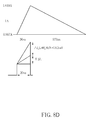
- FIG. 8D illustrates a schematic diagram of another practical measurement of the current sensing module 208 according to an embodiment of the invention.
- the embodiment shown in FIG. 8D changes the output voltage to be 0.15V and the 3% duty cycle signal D (i.e. the conduction periods of the up-bridge circuit and the down-bridge circuit are 30 ns and 970 ns, respectively).
- the peak current I_UP and the valley current I_DN are 1.033 A and 0.967 A, respectively.
- the sensing voltage should be 13.2 mV.
- the current sensing module 208 as well as the simulation sensing current source 80 in the embodiment of the invention are not affected by changes of the smaller output voltage corresponding to the decreasing duty cycle signal D, and the current sensing module 208 still transmits the sensing voltage SSV to the pulse width modulation comparator 214 .
- the sensing voltage SSV outputted by the current sensing module 208 of the invention is not affected by changes of the inductance value or the voltage value of the output terminal.
- the product application of the voltage converter apparatus 20 has broadened to provide accurate sensing voltage S_SV.
- the current sensing module 208 of the voltage converter apparatus 20 measuring the conduction currents of the switch transistor SWP or SWN to correspondingly output the pulse width modulation signal S_PWM can be summarized as a current sensing process 90 , as shown in FIG. 9 .
- the current sensing process 90 includes the steps as follows:
- Step 900 Start.
- Step 902 The circuit selection module 2080 compares the clock signal SCLK and the duty cycle signal S_Duty to generate the circuit selection result S_DCS.
- Step 904 According to the circuit selection result SDCS, the up-bridge sensing module 2082 _UP and the down-bridge sensing module 2082 _DN are selected to measure the conduction current of the switch transistor SWP or the switch transistor SWN.
- the up-bridge sensing module 2082 _UP measures the up-bridge conduction current ISENP.
- the down-bridge sensing module 2082 _DN measures the down-bridge conduction current ISENN.
- Step 906 According to the up-bridge conduction current ISENP and the down-bridge conduction current ISENN, the output module 406 generates the sensing result S_DNS of the currents passing through the inductor.
- Step 908 According to the sensing result SDNS and the slope compensation current SISL, the current generation module 2084 generates the sensing voltage SSV.
- Step 910 According the compensation result EAO and the sensing voltage S_SV, the pulse width modulation comparator 214 generates the pulse width modulation signal S_PWM.
- Step 912 End.
- the process of the voltage converter apparatus 20 transforming the input voltage VIN into the output voltage VOUT can be summarized as a voltage transformation process 70 , as shown in FIG. 10 .
- the voltage transformation process 70 includes the steps as follows:
- Step 700 Start.
- Step 702 The controller 200 receives the pulse width modulation signal SPWM and the clock signal SCLK to generate the duty cycle signal S_Duty.
- Step 704 According to the duty cycle signal S_Duty, the gate driver 201 generates the gate control signal S_G.
- Step 706 According to the gate control signal S_G, the driver circuit 202 controls the conduction conditions of the switch transistors SWP and SWN.
- Step 708 According to the conduction conditions of the switch transistors SWP and SWN, the capacitor COUT and the inductor L 1 are utilized to generate frequency response to transform the input voltage VIN into the output voltage VOUT.
- Step 710 End.
- the current sensing module 208 of the invention compares the duty cycle signal S_Duty and the clock signal SCLK to correspondingly select the up-bridge sensing module 2082 _UP or the down-bridge sensing module 2082 _DN, so as to measure the up-bridge conduction current ISENP of the switch transistor SWP or the down-bridge conduction current ISENN of the switch transistor SWN.
- those skilled in the art can combine other voltage measurement modules based on the conception of the invention to simultaneously measure the voltage changes of the switch transistors SWP, SWN to be transformed into the changes of the current, which is also in the scope of the invention.
- the embodiment of the invention mainly focuses on the conduction period of the switch transistor SWP being too short, and accordingly, the down-bridge conduction current ISENN of the switch transistor SWN can be measured and copied to reconstruct the sensing voltage S_SV.
- the invention provides a current sensing module for a voltage converter apparatus.
- a circuit selection module is utilized to determine a current sensing module for correspondingly measuring an up-bridge conduction current or a down-bridge conduction current. Then, according to a slope compensation current and the up-bridge/down-bridge conduction current, a current generation module generates a sensing voltage to adjust a duty cycle signal of the voltage converter apparatus, so as to improve the voltage transformation efficiency of the voltage converter apparatus and to adaptively measure the conduction currents of the voltage converter apparatus.
- the current sensing module sets up a simulation sensing current source to be automatically adjusted according to changes of the input/output terminal voltage value or the inductance of the inductor, so as to avoid unexpected changes of the input/output terminal voltage value or the inductances to limiting product application of the voltage converter apparatus
Landscapes
- Engineering & Computer Science (AREA)
- Power Engineering (AREA)
- Dc-Dc Converters (AREA)
Abstract
Description
the current difference ΔI_L is 204 mA. Then, according to another formula S_SV=ΔI_L×R_SEN, the practical sensing voltage S_SV is 40.8 mV. Lastly, according to another formula C_SEN×S_SV=ΔI_S×D, a simulation sensing capacitance C_SEN is 0.5 uF, and a model of a simulation sensing current source ΔI_S=204
is utilized to obtain the current difference ΔI_L to be 450 mA. Then, the formula S_SV=ΔI_L×R_SEN is utilized to obtain the practical sensing voltage S_SV to be 90 mV. Lastly, the simulation sensing capacitance C_SEN of 0.5 uF and ΔI_S=450 mA shown in
is utilized to obtain the current different ΔI_L to be 363 mA. Then, the formula S_SV=ΔI_L×R_SEN is utilized to obtain the practical sensing voltage S_SV to be 72.7 mV. Lastly, the simulation sensing capacitance C_SEN of 0.5 uF shown in
When the periodic period S_Duty changes, the current difference ΔI_S is required to be adjusted to the adjustment current difference ΔI_AS. Then, the formula C_SEN×S_SV=ΔI_AS×D is utilized to obtain the sensing voltage S_SV to be 72.7 mV, such as the embodiment shown in
is utilized to obtain the current different ΔI_L to be 66 mA. Then, the formula S_SV=ΔI_L×R_SEN is utilized to obtain the practical sensing voltage S_SV to be 13.2 mV. Lastly, the simulation sensing capacitance C_SEN of 0.5 uF shown in
and the formula C_SEN×S_SV=ΔI_AS×D, the sensing voltage should be 13.2 mV. In other words, the
Claims (18)
Applications Claiming Priority (3)
| Application Number | Priority Date | Filing Date | Title |
|---|---|---|---|
| TW101116166A | 2012-05-07 | ||
| TW101116166A TWI457740B (en) | 2012-05-07 | 2012-05-07 | Current sensing apparatus and voltage converter apparatus |
| TW101116166 | 2012-05-07 |
Publications (2)
| Publication Number | Publication Date |
|---|---|
| US20130293211A1 US20130293211A1 (en) | 2013-11-07 |
| US8922186B2 true US8922186B2 (en) | 2014-12-30 |
Family
ID=49512059
Family Applications (1)
| Application Number | Title | Priority Date | Filing Date |
|---|---|---|---|
| US13/628,025 Active 2033-06-18 US8922186B2 (en) | 2012-05-07 | 2012-09-26 | Method and apparatus for all duty current sensing in current mode converter |
Country Status (2)
| Country | Link |
|---|---|
| US (1) | US8922186B2 (en) |
| TW (1) | TWI457740B (en) |
Cited By (3)
| Publication number | Priority date | Publication date | Assignee | Title |
|---|---|---|---|---|
| US20220360171A1 (en) * | 2021-05-07 | 2022-11-10 | Texas Instruments Incorporated | Valley current mode control for a voltage converter |
| US11742741B2 (en) | 2020-09-08 | 2023-08-29 | Analog Devices International Unlimited Company | Spurious noise reduction by monotonic frequency stepping with compensation of error amplifier's output in peak current mode switching regulator |
| US11973424B2 (en) | 2020-09-08 | 2024-04-30 | Analog Devices International Unlimited Company | Spur free switching regulator with self-adaptive cancellation of coil current ripple |
Families Citing this family (43)
| Publication number | Priority date | Publication date | Assignee | Title |
|---|---|---|---|---|
| JP2012191821A (en) * | 2011-03-14 | 2012-10-04 | Toshiba Corp | Current direction detection circuit and dc-dc converter |
| JP5865028B2 (en) * | 2011-11-17 | 2016-02-17 | ルネサスエレクトロニクス株式会社 | DC-DC converter |
| MX341538B (en) * | 2011-12-31 | 2016-08-24 | Broad-Ocean Motor Ev Co Ltd | Narrow pulse filter circuit with automatic compensation and motor controller applying same. |
| US20140084884A1 (en) * | 2012-07-06 | 2014-03-27 | Jong J. Lee | Lc switching regulators |
| TWI465023B (en) * | 2012-09-18 | 2014-12-11 | Upi Semiconductor Corp | Power converter and operating method thereof |
| US9059594B2 (en) * | 2012-11-28 | 2015-06-16 | Energy Pass Incorporation | Battery switching charger and method for controlling battery switching charger |
| TWI487261B (en) * | 2013-11-20 | 2015-06-01 | Anpec Electronics Corp | Electronic system, voltage conversion circuit and method thereof |
| US9531284B2 (en) * | 2014-01-30 | 2016-12-27 | Silicon Laboratories Inc. | Pseudo-constant frequency control for voltage converter |
| US9531253B2 (en) | 2014-01-30 | 2016-12-27 | Silicon Laboratories Inc. | Soft-start for isolated power converter |
| US9929675B2 (en) * | 2014-02-26 | 2018-03-27 | Fsp Technology Inc. | Inverter apparatus capable of controlling burst mode operation and control method thereof |
| CN103997206B (en) * | 2014-05-20 | 2017-04-12 | 华为技术有限公司 | Switching power source |
| JP6307398B2 (en) * | 2014-09-24 | 2018-04-04 | ローム株式会社 | Current mode controlled switching power supply |
| JP6307400B2 (en) * | 2014-09-24 | 2018-04-04 | ローム株式会社 | Current mode controlled switching power supply |
| JP6329047B2 (en) * | 2014-09-24 | 2018-05-23 | ローム株式会社 | Current mode controlled switching power supply |
| US10076963B2 (en) | 2014-09-24 | 2018-09-18 | Rohm Co., Ltd. | Current mode control type switching power supply device |
| JP6307399B2 (en) * | 2014-09-24 | 2018-04-04 | ローム株式会社 | Current mode controlled switching power supply |
| JP6307401B2 (en) | 2014-09-24 | 2018-04-04 | ローム株式会社 | Current mode controlled switching power supply |
| TWI555318B (en) | 2015-05-13 | 2016-10-21 | 杰力科技股份有限公司 | Voltage converter |
| CN105226945B (en) * | 2015-10-16 | 2017-09-12 | 深圳宝砾微电子有限公司 | Boost chip |
| US10680522B2 (en) * | 2017-02-09 | 2020-06-09 | Rohm Co., Ltd. | Switching regulator and control device therefor |
| DE102017210507B4 (en) * | 2017-06-22 | 2019-06-27 | Dialog Semiconductor (Uk) Limited | Peak current control for a power switch of a power converter |
| US10353015B2 (en) * | 2017-07-24 | 2019-07-16 | Lg Chem, Ltd. | Diagnostic system for a DC-DC voltage converter |
| CN107742983B (en) * | 2017-11-29 | 2023-05-26 | 上海南麟电子股份有限公司 | Commonly compensated constant current and constant voltage control module, step-down circuit and compensation method |
| DE102018101932A1 (en) * | 2018-01-29 | 2019-08-01 | Infineon Technologies Ag | Switching converter that uses pulse frequency modulation and current operation control |
| JP6473253B2 (en) * | 2018-03-12 | 2019-02-20 | ローム株式会社 | Current mode controlled switching power supply |
| JP6471251B2 (en) * | 2018-03-12 | 2019-02-13 | ローム株式会社 | Current mode controlled switching power supply |
| JP6553226B2 (en) * | 2018-03-12 | 2019-07-31 | ローム株式会社 | Current mode controlled switching power supply |
| JP6449499B2 (en) * | 2018-03-12 | 2019-01-09 | ローム株式会社 | Current mode controlled switching power supply |
| JP6449502B2 (en) * | 2018-04-19 | 2019-01-09 | ローム株式会社 | Current mode controlled switching power supply |
| WO2019200900A1 (en) * | 2018-04-20 | 2019-10-24 | 晶晨半导体(上海)股份有限公司 | Power supply system having stable loop circuit |
| CN108599535A (en) * | 2018-07-09 | 2018-09-28 | 成都信息工程大学 | A kind of self-adaptable slop compensation circuit suitable for Peak Current Mode BUCK converters |
| US10992229B2 (en) * | 2018-10-17 | 2021-04-27 | Texas Instruments Incorporated | Comparator with preamplifier gain adjustment based on overdrive voltage |
| JP6764492B2 (en) * | 2019-01-24 | 2020-09-30 | ローム株式会社 | Current mode control type switching power supply |
| TWI683514B (en) * | 2019-05-10 | 2020-01-21 | 茂達電子股份有限公司 | Fast transient current mode control circuit and method |
| TWI722905B (en) * | 2020-05-22 | 2021-03-21 | 茂達電子股份有限公司 | Inductor current detecting circuit |
| TW202144804A (en) * | 2020-05-22 | 2021-12-01 | 茂達電子股份有限公司 | Inductor current detecting circuit |
| CN116057691A (en) * | 2021-02-12 | 2023-05-02 | 富士电机株式会社 | semiconductor module |
| TW202326337A (en) * | 2021-12-17 | 2023-07-01 | 力智電子股份有限公司 | Smart power stage circuit of power converter and current monitoring circuit thereof |
| CN115174431B (en) * | 2022-06-30 | 2023-09-05 | 无锡融卡科技有限公司 | Simple SWP full duplex logic signal acquisition device and method |
| CN115208190B (en) * | 2022-09-13 | 2022-12-20 | 深圳英集芯科技股份有限公司 | DCDC converter, switching power supply and electronic equipment |
| TWI812471B (en) * | 2022-09-19 | 2023-08-11 | 茂達電子股份有限公司 | Open-loop circuit of simulating inductor current |
| JPWO2024070219A1 (en) * | 2022-09-28 | 2024-04-04 | ||
| TWI847312B (en) * | 2022-10-20 | 2024-07-01 | 晶豪科技股份有限公司 | Control circuit with automatic frequency modulation for dc-dc converter |
Citations (15)
| Publication number | Priority date | Publication date | Assignee | Title |
|---|---|---|---|---|
| US4661766A (en) | 1985-12-23 | 1987-04-28 | Caterpillar Inc. | Dual current sensing driver circuit |
| US4967309A (en) | 1989-12-26 | 1990-10-30 | Caterpillar Inc. | Dual current sensing driver circuit |
| TWM244644U (en) | 2003-04-29 | 2004-09-21 | Niko Semiconductor Co Ltd | Current detection circuit of fly-back switching power supply |
| US6853174B1 (en) * | 2003-08-11 | 2005-02-08 | Micrel, Inc. | Selective high-side and low-side current sensing in switching power supplies |
| EP1503490B1 (en) | 2003-08-01 | 2006-10-18 | Infineon Technologies AG | Current sensing circuit |
| US7176665B2 (en) | 2004-06-14 | 2007-02-13 | Dialog Semiconductor Gmbh | Analog current sense circuit |
| TW200951667A (en) | 2008-06-02 | 2009-12-16 | Addtek Corp | Current sensing circuit |
| TW201003082A (en) | 2008-04-01 | 2010-01-16 | O2Micro Inc | Circuits, systems and methods for current sensing |
| TW201005464A (en) | 2008-07-24 | 2010-02-01 | Ite Tech Inc | Power converter and current dectection apparatus thereof |
| US20100026262A1 (en) * | 2008-07-30 | 2010-02-04 | Takashi Sase | Power Supplying Apparatus |
| US7936160B1 (en) * | 2007-04-25 | 2011-05-03 | National Semiconductor Corporation | Apparatus and method for valley emulated current mode control |
| TW201118523A (en) | 2009-11-17 | 2011-06-01 | Analogtek Corp | Current detection and control circuit |
| US7990118B2 (en) * | 2007-08-16 | 2011-08-02 | Fitipower Integrated Technology, Inc. | Switching regulator with high efficiency in light load mode |
| US20110241641A1 (en) * | 2010-04-06 | 2011-10-06 | Chih-Ning Chen | Current Mode Buck Converter with Fixed PWM/PFM Boundary |
| US20110279048A1 (en) | 2010-05-11 | 2011-11-17 | Arkalumen Inc. | Circuits for sensing current levels within lighting apparatus |
-
2012
- 2012-05-07 TW TW101116166A patent/TWI457740B/en active
- 2012-09-26 US US13/628,025 patent/US8922186B2/en active Active
Patent Citations (15)
| Publication number | Priority date | Publication date | Assignee | Title |
|---|---|---|---|---|
| US4661766A (en) | 1985-12-23 | 1987-04-28 | Caterpillar Inc. | Dual current sensing driver circuit |
| US4967309A (en) | 1989-12-26 | 1990-10-30 | Caterpillar Inc. | Dual current sensing driver circuit |
| TWM244644U (en) | 2003-04-29 | 2004-09-21 | Niko Semiconductor Co Ltd | Current detection circuit of fly-back switching power supply |
| EP1503490B1 (en) | 2003-08-01 | 2006-10-18 | Infineon Technologies AG | Current sensing circuit |
| US6853174B1 (en) * | 2003-08-11 | 2005-02-08 | Micrel, Inc. | Selective high-side and low-side current sensing in switching power supplies |
| US7176665B2 (en) | 2004-06-14 | 2007-02-13 | Dialog Semiconductor Gmbh | Analog current sense circuit |
| US7936160B1 (en) * | 2007-04-25 | 2011-05-03 | National Semiconductor Corporation | Apparatus and method for valley emulated current mode control |
| US7990118B2 (en) * | 2007-08-16 | 2011-08-02 | Fitipower Integrated Technology, Inc. | Switching regulator with high efficiency in light load mode |
| TW201003082A (en) | 2008-04-01 | 2010-01-16 | O2Micro Inc | Circuits, systems and methods for current sensing |
| TW200951667A (en) | 2008-06-02 | 2009-12-16 | Addtek Corp | Current sensing circuit |
| TW201005464A (en) | 2008-07-24 | 2010-02-01 | Ite Tech Inc | Power converter and current dectection apparatus thereof |
| US20100026262A1 (en) * | 2008-07-30 | 2010-02-04 | Takashi Sase | Power Supplying Apparatus |
| TW201118523A (en) | 2009-11-17 | 2011-06-01 | Analogtek Corp | Current detection and control circuit |
| US20110241641A1 (en) * | 2010-04-06 | 2011-10-06 | Chih-Ning Chen | Current Mode Buck Converter with Fixed PWM/PFM Boundary |
| US20110279048A1 (en) | 2010-05-11 | 2011-11-17 | Arkalumen Inc. | Circuits for sensing current levels within lighting apparatus |
Cited By (4)
| Publication number | Priority date | Publication date | Assignee | Title |
|---|---|---|---|---|
| US11742741B2 (en) | 2020-09-08 | 2023-08-29 | Analog Devices International Unlimited Company | Spurious noise reduction by monotonic frequency stepping with compensation of error amplifier's output in peak current mode switching regulator |
| US11973424B2 (en) | 2020-09-08 | 2024-04-30 | Analog Devices International Unlimited Company | Spur free switching regulator with self-adaptive cancellation of coil current ripple |
| US20220360171A1 (en) * | 2021-05-07 | 2022-11-10 | Texas Instruments Incorporated | Valley current mode control for a voltage converter |
| US11722061B2 (en) * | 2021-05-07 | 2023-08-08 | Texas Instruments Incorporated | Valley current mode control for a voltage converter |
Also Published As
| Publication number | Publication date |
|---|---|
| US20130293211A1 (en) | 2013-11-07 |
| TWI457740B (en) | 2014-10-21 |
| TW201346479A (en) | 2013-11-16 |
Similar Documents
| Publication | Publication Date | Title |
|---|---|---|
| US8922186B2 (en) | Method and apparatus for all duty current sensing in current mode converter | |
| US8779733B2 (en) | Bootstrap scheme for BULK-BOOST converter | |
| US7876073B2 (en) | Switching regulator with slope compensation and control method therefor | |
| US7605573B2 (en) | Switching regulator providing slope compensation and voltage control method thereof | |
| US7180274B2 (en) | Switching voltage regulator operating without a discontinuous mode | |
| US11381167B2 (en) | Power converter with slope compensation | |
| JP6889078B2 (en) | Switching power supply | |
| TWI479790B (en) | Switching-mode power supply with ripple mode control and associated methods | |
| US8330442B2 (en) | DC to DC converter and method for reducing overshoot | |
| US8994352B2 (en) | Switching regulator and control method for same | |
| US20100194369A1 (en) | Dc-dc converter and switching control circuit | |
| JP5723578B2 (en) | Switching power supply | |
| US20210119533A1 (en) | Dc-dc converter with current loop gain | |
| CN102931841A (en) | Multiphase DC-DC Power Converter | |
| JP2013165537A (en) | Switching regulator, control method therefor, and power supply device | |
| CN102742135A (en) | Buck-boost DC-DC converter and switch control circuit | |
| JP2010068553A (en) | Current-mode control type dc-dc converter | |
| JP2008131746A (en) | Buck-boost switching regulator | |
| US12244229B2 (en) | Inductor current reconstruction circuit, power converter and inductor current reconstruction method thereof | |
| US7705569B2 (en) | Slope rate compensation circuit, method thereof and pulse width modulation boost converter circuit | |
| US7859242B2 (en) | DC-DC Converter | |
| US7274182B2 (en) | Spring modulation with fast load-transient response for a voltage regulator | |
| JP2019071715A (en) | Switching regulator | |
| CN109256948B (en) | Switching regulator | |
| US12068688B2 (en) | Switching power supply device |
Legal Events
| Date | Code | Title | Description |
|---|---|---|---|
| AS | Assignment |
Owner name: ANPEC ELECTRONICS CORPORATION, TAIWAN Free format text: ASSIGNMENT OF ASSIGNORS INTEREST;ASSIGNOR:CHEN, CHIH-NING;REEL/FRAME:029033/0758 Effective date: 20120919 |
|
| STCF | Information on status: patent grant |
Free format text: PATENTED CASE |
|
| MAFP | Maintenance fee payment |
Free format text: PAYMENT OF MAINTENANCE FEE, 4TH YR, SMALL ENTITY (ORIGINAL EVENT CODE: M2551) Year of fee payment: 4 |
|
| MAFP | Maintenance fee payment |
Free format text: PAYMENT OF MAINTENANCE FEE, 8TH YR, SMALL ENTITY (ORIGINAL EVENT CODE: M2552); ENTITY STATUS OF PATENT OWNER: SMALL ENTITY Year of fee payment: 8 |