US8916433B2 - Superior integrity of high-k metal gate stacks by capping STI regions - Google Patents
Superior integrity of high-k metal gate stacks by capping STI regions Download PDFInfo
- Publication number
- US8916433B2 US8916433B2 US13/406,869 US201213406869A US8916433B2 US 8916433 B2 US8916433 B2 US 8916433B2 US 201213406869 A US201213406869 A US 201213406869A US 8916433 B2 US8916433 B2 US 8916433B2
- Authority
- US
- United States
- Prior art keywords
- layer
- forming
- mask layer
- dielectric material
- semiconductor
- Prior art date
- Legal status (The legal status is an assumption and is not a legal conclusion. Google has not performed a legal analysis and makes no representation as to the accuracy of the status listed.)
- Active, expires
Links
- 229910052751 metal Inorganic materials 0.000 title claims abstract description 32
- 239000002184 metal Substances 0.000 title claims abstract description 32
- 239000000463 material Substances 0.000 claims abstract description 114
- 238000002955 isolation Methods 0.000 claims abstract description 62
- VYPSYNLAJGMNEJ-UHFFFAOYSA-N Silicium dioxide Chemical compound O=[Si]=O VYPSYNLAJGMNEJ-UHFFFAOYSA-N 0.000 claims abstract description 38
- 239000000377 silicon dioxide Substances 0.000 claims abstract description 18
- 235000012239 silicon dioxide Nutrition 0.000 claims abstract description 18
- 238000000034 method Methods 0.000 claims description 107
- 239000004065 semiconductor Substances 0.000 claims description 105
- 239000003989 dielectric material Substances 0.000 claims description 82
- 230000008569 process Effects 0.000 claims description 56
- 230000001939 inductive effect Effects 0.000 claims description 23
- 229910045601 alloy Inorganic materials 0.000 claims description 22
- 239000000956 alloy Substances 0.000 claims description 22
- 239000007772 electrode material Substances 0.000 claims description 19
- 239000010703 silicon Substances 0.000 claims description 18
- 238000000151 deposition Methods 0.000 claims description 12
- 239000000126 substance Substances 0.000 claims description 11
- 229910052581 Si3N4 Inorganic materials 0.000 claims description 10
- HQVNEWCFYHHQES-UHFFFAOYSA-N silicon nitride Chemical compound N12[Si]34N5[Si]62N3[Si]51N64 HQVNEWCFYHHQES-UHFFFAOYSA-N 0.000 claims description 10
- 238000009413 insulation Methods 0.000 claims description 9
- 239000000203 mixture Substances 0.000 claims description 9
- 238000005530 etching Methods 0.000 claims description 8
- 229910052710 silicon Inorganic materials 0.000 claims description 7
- 238000000059 patterning Methods 0.000 claims description 6
- 238000007517 polishing process Methods 0.000 claims description 6
- 230000001681 protective effect Effects 0.000 claims description 6
- 229910052799 carbon Inorganic materials 0.000 claims description 3
- GNPVGFCGXDBREM-UHFFFAOYSA-N germanium atom Chemical compound [Ge] GNPVGFCGXDBREM-UHFFFAOYSA-N 0.000 claims description 3
- 229910052814 silicon oxide Inorganic materials 0.000 claims description 3
- 229910052732 germanium Inorganic materials 0.000 claims description 2
- QJGQUHMNIGDVPM-UHFFFAOYSA-N nitrogen group Chemical group [N] QJGQUHMNIGDVPM-UHFFFAOYSA-N 0.000 claims description 2
- 239000010410 layer Substances 0.000 claims 91
- 239000002355 dual-layer Substances 0.000 claims 7
- OKTJSMMVPCPJKN-UHFFFAOYSA-N Carbon Chemical compound [C] OKTJSMMVPCPJKN-UHFFFAOYSA-N 0.000 claims 1
- ATJFFYVFTNAWJD-UHFFFAOYSA-N Tin Chemical compound [Sn] ATJFFYVFTNAWJD-UHFFFAOYSA-N 0.000 claims 1
- 229910052718 tin Inorganic materials 0.000 claims 1
- 238000004519 manufacturing process Methods 0.000 abstract description 26
- 238000012876 topography Methods 0.000 abstract description 15
- 238000005538 encapsulation Methods 0.000 abstract description 7
- XUIMIQQOPSSXEZ-UHFFFAOYSA-N Silicon Chemical compound [Si] XUIMIQQOPSSXEZ-UHFFFAOYSA-N 0.000 description 16
- 238000004140 cleaning Methods 0.000 description 14
- 125000006850 spacer group Chemical group 0.000 description 13
- 238000012545 processing Methods 0.000 description 11
- 229910000676 Si alloy Inorganic materials 0.000 description 10
- 230000005669 field effect Effects 0.000 description 10
- 229910000927 Ge alloy Inorganic materials 0.000 description 9
- KRHYYFGTRYWZRS-UHFFFAOYSA-N Fluorane Chemical compound F KRHYYFGTRYWZRS-UHFFFAOYSA-N 0.000 description 8
- 230000000875 corresponding effect Effects 0.000 description 8
- 230000008021 deposition Effects 0.000 description 8
- 230000001965 increasing effect Effects 0.000 description 8
- 230000007246 mechanism Effects 0.000 description 8
- 230000002829 reductive effect Effects 0.000 description 8
- 239000000758 substrate Substances 0.000 description 8
- 238000013461 design Methods 0.000 description 6
- 230000003628 erosive effect Effects 0.000 description 6
- WIHZLLGSGQNAGK-UHFFFAOYSA-N hafnium(4+);oxygen(2-) Chemical compound [O-2].[O-2].[Hf+4] WIHZLLGSGQNAGK-UHFFFAOYSA-N 0.000 description 5
- 238000010348 incorporation Methods 0.000 description 5
- 229910021420 polycrystalline silicon Inorganic materials 0.000 description 5
- 229920005591 polysilicon Polymers 0.000 description 5
- 239000002800 charge carrier Substances 0.000 description 4
- 238000005229 chemical vapour deposition Methods 0.000 description 4
- 229910000449 hafnium oxide Inorganic materials 0.000 description 4
- 239000002210 silicon-based material Substances 0.000 description 4
- LYCAIKOWRPUZTN-UHFFFAOYSA-N Ethylene glycol Chemical compound OCCO LYCAIKOWRPUZTN-UHFFFAOYSA-N 0.000 description 3
- NRTOMJZYCJJWKI-UHFFFAOYSA-N Titanium nitride Chemical compound [Ti]#N NRTOMJZYCJJWKI-UHFFFAOYSA-N 0.000 description 3
- 230000006978 adaptation Effects 0.000 description 3
- 238000013459 approach Methods 0.000 description 3
- 238000005516 engineering process Methods 0.000 description 3
- 238000001459 lithography Methods 0.000 description 3
- 230000000873 masking effect Effects 0.000 description 3
- 230000009467 reduction Effects 0.000 description 3
- IJGRMHOSHXDMSA-UHFFFAOYSA-N Atomic nitrogen Chemical compound N#N IJGRMHOSHXDMSA-UHFFFAOYSA-N 0.000 description 2
- MHAJPDPJQMAIIY-UHFFFAOYSA-N Hydrogen peroxide Chemical compound OO MHAJPDPJQMAIIY-UHFFFAOYSA-N 0.000 description 2
- 229910001128 Sn alloy Inorganic materials 0.000 description 2
- QAOWNCQODCNURD-UHFFFAOYSA-N Sulfuric acid Chemical compound OS(O)(=O)=O QAOWNCQODCNURD-UHFFFAOYSA-N 0.000 description 2
- 230000008901 benefit Effects 0.000 description 2
- 230000015572 biosynthetic process Effects 0.000 description 2
- 230000008878 coupling Effects 0.000 description 2
- 238000010168 coupling process Methods 0.000 description 2
- 238000005859 coupling reaction Methods 0.000 description 2
- 230000006866 deterioration Effects 0.000 description 2
- 238000011161 development Methods 0.000 description 2
- 239000002019 doping agent Substances 0.000 description 2
- 239000011810 insulating material Substances 0.000 description 2
- 238000012986 modification Methods 0.000 description 2
- 230000004048 modification Effects 0.000 description 2
- QPJSUIGXIBEQAC-UHFFFAOYSA-N n-(2,4-dichloro-5-propan-2-yloxyphenyl)acetamide Chemical compound CC(C)OC1=CC(NC(C)=O)=C(Cl)C=C1Cl QPJSUIGXIBEQAC-UHFFFAOYSA-N 0.000 description 2
- 230000003647 oxidation Effects 0.000 description 2
- 238000007254 oxidation reaction Methods 0.000 description 2
- 230000003068 static effect Effects 0.000 description 2
- 229910001339 C alloy Inorganic materials 0.000 description 1
- 229910052782 aluminium Inorganic materials 0.000 description 1
- XAGFODPZIPBFFR-UHFFFAOYSA-N aluminium Chemical compound [Al] XAGFODPZIPBFFR-UHFFFAOYSA-N 0.000 description 1
- 239000002194 amorphous carbon material Substances 0.000 description 1
- 239000012298 atmosphere Substances 0.000 description 1
- 239000006227 byproduct Substances 0.000 description 1
- 239000012876 carrier material Substances 0.000 description 1
- 239000003795 chemical substances by application Substances 0.000 description 1
- 239000012459 cleaning agent Substances 0.000 description 1
- 239000011365 complex material Substances 0.000 description 1
- 238000010276 construction Methods 0.000 description 1
- 239000000356 contaminant Substances 0.000 description 1
- 230000001276 controlling effect Effects 0.000 description 1
- 230000002596 correlated effect Effects 0.000 description 1
- 230000001627 detrimental effect Effects 0.000 description 1
- 230000000694 effects Effects 0.000 description 1
- 230000002708 enhancing effect Effects 0.000 description 1
- 238000010438 heat treatment Methods 0.000 description 1
- 230000006872 improvement Effects 0.000 description 1
- 239000012212 insulator Substances 0.000 description 1
- 229910052746 lanthanum Inorganic materials 0.000 description 1
- FZLIPJUXYLNCLC-UHFFFAOYSA-N lanthanum atom Chemical compound [La] FZLIPJUXYLNCLC-UHFFFAOYSA-N 0.000 description 1
- 238000004518 low pressure chemical vapour deposition Methods 0.000 description 1
- 150000002739 metals Chemical class 0.000 description 1
- 229910052757 nitrogen Inorganic materials 0.000 description 1
- TWNQGVIAIRXVLR-UHFFFAOYSA-N oxo(oxoalumanyloxy)alumane Chemical compound O=[Al]O[Al]=O TWNQGVIAIRXVLR-UHFFFAOYSA-N 0.000 description 1
- RVTZCBVAJQQJTK-UHFFFAOYSA-N oxygen(2-);zirconium(4+) Chemical compound [O-2].[O-2].[Zr+4] RVTZCBVAJQQJTK-UHFFFAOYSA-N 0.000 description 1
- 238000012856 packing Methods 0.000 description 1
- 238000005268 plasma chemical vapour deposition Methods 0.000 description 1
- 238000002360 preparation method Methods 0.000 description 1
- 150000003376 silicon Chemical class 0.000 description 1
- 238000003860 storage Methods 0.000 description 1
- 229910052715 tantalum Inorganic materials 0.000 description 1
- GUVRBAGPIYLISA-UHFFFAOYSA-N tantalum atom Chemical compound [Ta] GUVRBAGPIYLISA-UHFFFAOYSA-N 0.000 description 1
- MZLGASXMSKOWSE-UHFFFAOYSA-N tantalum nitride Chemical compound [Ta]#N MZLGASXMSKOWSE-UHFFFAOYSA-N 0.000 description 1
- 230000005641 tunneling Effects 0.000 description 1
- 229910001928 zirconium oxide Inorganic materials 0.000 description 1
Images


Classifications
-
- H—ELECTRICITY
- H01—ELECTRIC ELEMENTS
- H01L—SEMICONDUCTOR DEVICES NOT COVERED BY CLASS H10
- H01L21/00—Processes or apparatus adapted for the manufacture or treatment of semiconductor or solid state devices or of parts thereof
- H01L21/70—Manufacture or treatment of devices consisting of a plurality of solid state components formed in or on a common substrate or of parts thereof; Manufacture of integrated circuit devices or of parts thereof
- H01L21/77—Manufacture or treatment of devices consisting of a plurality of solid state components or integrated circuits formed in, or on, a common substrate
- H01L21/78—Manufacture or treatment of devices consisting of a plurality of solid state components or integrated circuits formed in, or on, a common substrate with subsequent division of the substrate into plural individual devices
- H01L21/82—Manufacture or treatment of devices consisting of a plurality of solid state components or integrated circuits formed in, or on, a common substrate with subsequent division of the substrate into plural individual devices to produce devices, e.g. integrated circuits, each consisting of a plurality of components
- H01L21/822—Manufacture or treatment of devices consisting of a plurality of solid state components or integrated circuits formed in, or on, a common substrate with subsequent division of the substrate into plural individual devices to produce devices, e.g. integrated circuits, each consisting of a plurality of components the substrate being a semiconductor, using silicon technology
- H01L21/8232—Field-effect technology
- H01L21/8234—MIS technology, i.e. integration processes of field effect transistors of the conductor-insulator-semiconductor type
- H01L21/8238—Complementary field-effect transistors, e.g. CMOS
- H01L21/823878—Complementary field-effect transistors, e.g. CMOS isolation region manufacturing related aspects, e.g. to avoid interaction of isolation region with adjacent structure
-
- H—ELECTRICITY
- H01—ELECTRIC ELEMENTS
- H01L—SEMICONDUCTOR DEVICES NOT COVERED BY CLASS H10
- H01L21/00—Processes or apparatus adapted for the manufacture or treatment of semiconductor or solid state devices or of parts thereof
- H01L21/02—Manufacture or treatment of semiconductor devices or of parts thereof
- H01L21/04—Manufacture or treatment of semiconductor devices or of parts thereof the devices having at least one potential-jump barrier or surface barrier, e.g. PN junction, depletion layer or carrier concentration layer
- H01L21/18—Manufacture or treatment of semiconductor devices or of parts thereof the devices having at least one potential-jump barrier or surface barrier, e.g. PN junction, depletion layer or carrier concentration layer the devices having semiconductor bodies comprising elements of Group IV of the Periodic System or AIIIBV compounds with or without impurities, e.g. doping materials
- H01L21/28—Manufacture of electrodes on semiconductor bodies using processes or apparatus not provided for in groups H01L21/20 - H01L21/268
- H01L21/28008—Making conductor-insulator-semiconductor electrodes
- H01L21/28017—Making conductor-insulator-semiconductor electrodes the insulator being formed after the semiconductor body, the semiconductor being silicon
- H01L21/28026—Making conductor-insulator-semiconductor electrodes the insulator being formed after the semiconductor body, the semiconductor being silicon characterised by the conductor
- H01L21/28123—Lithography-related aspects, e.g. sub-lithography lengths; Isolation-related aspects, e.g. to solve problems arising at the crossing with the side of the device isolation; Planarisation aspects
-
- H—ELECTRICITY
- H01—ELECTRIC ELEMENTS
- H01L—SEMICONDUCTOR DEVICES NOT COVERED BY CLASS H10
- H01L21/00—Processes or apparatus adapted for the manufacture or treatment of semiconductor or solid state devices or of parts thereof
- H01L21/70—Manufacture or treatment of devices consisting of a plurality of solid state components formed in or on a common substrate or of parts thereof; Manufacture of integrated circuit devices or of parts thereof
- H01L21/71—Manufacture of specific parts of devices defined in group H01L21/70
- H01L21/76—Making of isolation regions between components
- H01L21/762—Dielectric regions, e.g. EPIC dielectric isolation, LOCOS; Trench refilling techniques, SOI technology, use of channel stoppers
- H01L21/76224—Dielectric regions, e.g. EPIC dielectric isolation, LOCOS; Trench refilling techniques, SOI technology, use of channel stoppers using trench refilling with dielectric materials
- H01L21/76232—Dielectric regions, e.g. EPIC dielectric isolation, LOCOS; Trench refilling techniques, SOI technology, use of channel stoppers using trench refilling with dielectric materials of trenches having a shape other than rectangular or V-shape, e.g. rounded corners, oblique or rounded trench walls
-
- H—ELECTRICITY
- H01—ELECTRIC ELEMENTS
- H01L—SEMICONDUCTOR DEVICES NOT COVERED BY CLASS H10
- H01L21/00—Processes or apparatus adapted for the manufacture or treatment of semiconductor or solid state devices or of parts thereof
- H01L21/70—Manufacture or treatment of devices consisting of a plurality of solid state components formed in or on a common substrate or of parts thereof; Manufacture of integrated circuit devices or of parts thereof
- H01L21/77—Manufacture or treatment of devices consisting of a plurality of solid state components or integrated circuits formed in, or on, a common substrate
- H01L21/78—Manufacture or treatment of devices consisting of a plurality of solid state components or integrated circuits formed in, or on, a common substrate with subsequent division of the substrate into plural individual devices
- H01L21/82—Manufacture or treatment of devices consisting of a plurality of solid state components or integrated circuits formed in, or on, a common substrate with subsequent division of the substrate into plural individual devices to produce devices, e.g. integrated circuits, each consisting of a plurality of components
- H01L21/822—Manufacture or treatment of devices consisting of a plurality of solid state components or integrated circuits formed in, or on, a common substrate with subsequent division of the substrate into plural individual devices to produce devices, e.g. integrated circuits, each consisting of a plurality of components the substrate being a semiconductor, using silicon technology
- H01L21/8232—Field-effect technology
- H01L21/8234—MIS technology, i.e. integration processes of field effect transistors of the conductor-insulator-semiconductor type
- H01L21/823437—MIS technology, i.e. integration processes of field effect transistors of the conductor-insulator-semiconductor type with a particular manufacturing method of the gate conductors, e.g. particular materials, shapes
-
- H—ELECTRICITY
- H01—ELECTRIC ELEMENTS
- H01L—SEMICONDUCTOR DEVICES NOT COVERED BY CLASS H10
- H01L21/00—Processes or apparatus adapted for the manufacture or treatment of semiconductor or solid state devices or of parts thereof
- H01L21/70—Manufacture or treatment of devices consisting of a plurality of solid state components formed in or on a common substrate or of parts thereof; Manufacture of integrated circuit devices or of parts thereof
- H01L21/77—Manufacture or treatment of devices consisting of a plurality of solid state components or integrated circuits formed in, or on, a common substrate
- H01L21/78—Manufacture or treatment of devices consisting of a plurality of solid state components or integrated circuits formed in, or on, a common substrate with subsequent division of the substrate into plural individual devices
- H01L21/82—Manufacture or treatment of devices consisting of a plurality of solid state components or integrated circuits formed in, or on, a common substrate with subsequent division of the substrate into plural individual devices to produce devices, e.g. integrated circuits, each consisting of a plurality of components
- H01L21/822—Manufacture or treatment of devices consisting of a plurality of solid state components or integrated circuits formed in, or on, a common substrate with subsequent division of the substrate into plural individual devices to produce devices, e.g. integrated circuits, each consisting of a plurality of components the substrate being a semiconductor, using silicon technology
- H01L21/8232—Field-effect technology
- H01L21/8234—MIS technology, i.e. integration processes of field effect transistors of the conductor-insulator-semiconductor type
- H01L21/823481—MIS technology, i.e. integration processes of field effect transistors of the conductor-insulator-semiconductor type isolation region manufacturing related aspects, e.g. to avoid interaction of isolation region with adjacent structure
-
- H—ELECTRICITY
- H01—ELECTRIC ELEMENTS
- H01L—SEMICONDUCTOR DEVICES NOT COVERED BY CLASS H10
- H01L21/00—Processes or apparatus adapted for the manufacture or treatment of semiconductor or solid state devices or of parts thereof
- H01L21/70—Manufacture or treatment of devices consisting of a plurality of solid state components formed in or on a common substrate or of parts thereof; Manufacture of integrated circuit devices or of parts thereof
- H01L21/77—Manufacture or treatment of devices consisting of a plurality of solid state components or integrated circuits formed in, or on, a common substrate
- H01L21/78—Manufacture or treatment of devices consisting of a plurality of solid state components or integrated circuits formed in, or on, a common substrate with subsequent division of the substrate into plural individual devices
- H01L21/82—Manufacture or treatment of devices consisting of a plurality of solid state components or integrated circuits formed in, or on, a common substrate with subsequent division of the substrate into plural individual devices to produce devices, e.g. integrated circuits, each consisting of a plurality of components
- H01L21/822—Manufacture or treatment of devices consisting of a plurality of solid state components or integrated circuits formed in, or on, a common substrate with subsequent division of the substrate into plural individual devices to produce devices, e.g. integrated circuits, each consisting of a plurality of components the substrate being a semiconductor, using silicon technology
- H01L21/8232—Field-effect technology
- H01L21/8234—MIS technology, i.e. integration processes of field effect transistors of the conductor-insulator-semiconductor type
- H01L21/8238—Complementary field-effect transistors, e.g. CMOS
- H01L21/823828—Complementary field-effect transistors, e.g. CMOS with a particular manufacturing method of the gate conductors, e.g. particular materials, shapes
-
- H—ELECTRICITY
- H01—ELECTRIC ELEMENTS
- H01L—SEMICONDUCTOR DEVICES NOT COVERED BY CLASS H10
- H01L29/00—Semiconductor devices adapted for rectifying, amplifying, oscillating or switching, or capacitors or resistors with at least one potential-jump barrier or surface barrier, e.g. PN junction depletion layer or carrier concentration layer; Details of semiconductor bodies or of electrodes thereof ; Multistep manufacturing processes therefor
- H01L29/02—Semiconductor bodies ; Multistep manufacturing processes therefor
- H01L29/06—Semiconductor bodies ; Multistep manufacturing processes therefor characterised by their shape; characterised by the shapes, relative sizes, or dispositions of the semiconductor regions ; characterised by the concentration or distribution of impurities within semiconductor regions
- H01L29/10—Semiconductor bodies ; Multistep manufacturing processes therefor characterised by their shape; characterised by the shapes, relative sizes, or dispositions of the semiconductor regions ; characterised by the concentration or distribution of impurities within semiconductor regions with semiconductor regions connected to an electrode not carrying current to be rectified, amplified or switched and such electrode being part of a semiconductor device which comprises three or more electrodes
- H01L29/1025—Channel region of field-effect devices
- H01L29/1029—Channel region of field-effect devices of field-effect transistors
- H01L29/1033—Channel region of field-effect devices of field-effect transistors with insulated gate, e.g. characterised by the length, the width, the geometric contour or the doping structure
- H01L29/1054—Channel region of field-effect devices of field-effect transistors with insulated gate, e.g. characterised by the length, the width, the geometric contour or the doping structure with a variation of the composition, e.g. channel with strained layer for increasing the mobility
-
- H—ELECTRICITY
- H01—ELECTRIC ELEMENTS
- H01L—SEMICONDUCTOR DEVICES NOT COVERED BY CLASS H10
- H01L29/00—Semiconductor devices adapted for rectifying, amplifying, oscillating or switching, or capacitors or resistors with at least one potential-jump barrier or surface barrier, e.g. PN junction depletion layer or carrier concentration layer; Details of semiconductor bodies or of electrodes thereof ; Multistep manufacturing processes therefor
- H01L29/40—Electrodes ; Multistep manufacturing processes therefor
- H01L29/43—Electrodes ; Multistep manufacturing processes therefor characterised by the materials of which they are formed
- H01L29/49—Metal-insulator-semiconductor electrodes, e.g. gates of MOSFET
- H01L29/4966—Metal-insulator-semiconductor electrodes, e.g. gates of MOSFET the conductor material next to the insulator being a composite material, e.g. organic material, TiN, MoSi2
-
- H—ELECTRICITY
- H01—ELECTRIC ELEMENTS
- H01L—SEMICONDUCTOR DEVICES NOT COVERED BY CLASS H10
- H01L29/00—Semiconductor devices adapted for rectifying, amplifying, oscillating or switching, or capacitors or resistors with at least one potential-jump barrier or surface barrier, e.g. PN junction depletion layer or carrier concentration layer; Details of semiconductor bodies or of electrodes thereof ; Multistep manufacturing processes therefor
- H01L29/40—Electrodes ; Multistep manufacturing processes therefor
- H01L29/43—Electrodes ; Multistep manufacturing processes therefor characterised by the materials of which they are formed
- H01L29/49—Metal-insulator-semiconductor electrodes, e.g. gates of MOSFET
- H01L29/51—Insulating materials associated therewith
- H01L29/511—Insulating materials associated therewith with a compositional variation, e.g. multilayer structures
- H01L29/513—Insulating materials associated therewith with a compositional variation, e.g. multilayer structures the variation being perpendicular to the channel plane
-
- H—ELECTRICITY
- H01—ELECTRIC ELEMENTS
- H01L—SEMICONDUCTOR DEVICES NOT COVERED BY CLASS H10
- H01L29/00—Semiconductor devices adapted for rectifying, amplifying, oscillating or switching, or capacitors or resistors with at least one potential-jump barrier or surface barrier, e.g. PN junction depletion layer or carrier concentration layer; Details of semiconductor bodies or of electrodes thereof ; Multistep manufacturing processes therefor
- H01L29/66—Types of semiconductor device ; Multistep manufacturing processes therefor
- H01L29/68—Types of semiconductor device ; Multistep manufacturing processes therefor controllable by only the electric current supplied, or only the electric potential applied, to an electrode which does not carry the current to be rectified, amplified or switched
- H01L29/76—Unipolar devices, e.g. field effect transistors
- H01L29/772—Field effect transistors
- H01L29/78—Field effect transistors with field effect produced by an insulated gate
-
- H—ELECTRICITY
- H01—ELECTRIC ELEMENTS
- H01L—SEMICONDUCTOR DEVICES NOT COVERED BY CLASS H10
- H01L21/00—Processes or apparatus adapted for the manufacture or treatment of semiconductor or solid state devices or of parts thereof
- H01L21/70—Manufacture or treatment of devices consisting of a plurality of solid state components formed in or on a common substrate or of parts thereof; Manufacture of integrated circuit devices or of parts thereof
- H01L21/77—Manufacture or treatment of devices consisting of a plurality of solid state components or integrated circuits formed in, or on, a common substrate
- H01L21/78—Manufacture or treatment of devices consisting of a plurality of solid state components or integrated circuits formed in, or on, a common substrate with subsequent division of the substrate into plural individual devices
- H01L21/82—Manufacture or treatment of devices consisting of a plurality of solid state components or integrated circuits formed in, or on, a common substrate with subsequent division of the substrate into plural individual devices to produce devices, e.g. integrated circuits, each consisting of a plurality of components
- H01L21/822—Manufacture or treatment of devices consisting of a plurality of solid state components or integrated circuits formed in, or on, a common substrate with subsequent division of the substrate into plural individual devices to produce devices, e.g. integrated circuits, each consisting of a plurality of components the substrate being a semiconductor, using silicon technology
- H01L21/8232—Field-effect technology
- H01L21/8234—MIS technology, i.e. integration processes of field effect transistors of the conductor-insulator-semiconductor type
- H01L21/823418—MIS technology, i.e. integration processes of field effect transistors of the conductor-insulator-semiconductor type with a particular manufacturing method of the source or drain structures, e.g. specific source or drain implants or silicided source or drain structures or raised source or drain structures
- H01L21/823425—MIS technology, i.e. integration processes of field effect transistors of the conductor-insulator-semiconductor type with a particular manufacturing method of the source or drain structures, e.g. specific source or drain implants or silicided source or drain structures or raised source or drain structures manufacturing common source or drain regions between a plurality of conductor-insulator-semiconductor structures
-
- H—ELECTRICITY
- H01—ELECTRIC ELEMENTS
- H01L—SEMICONDUCTOR DEVICES NOT COVERED BY CLASS H10
- H01L29/00—Semiconductor devices adapted for rectifying, amplifying, oscillating or switching, or capacitors or resistors with at least one potential-jump barrier or surface barrier, e.g. PN junction depletion layer or carrier concentration layer; Details of semiconductor bodies or of electrodes thereof ; Multistep manufacturing processes therefor
- H01L29/66—Types of semiconductor device ; Multistep manufacturing processes therefor
- H01L29/68—Types of semiconductor device ; Multistep manufacturing processes therefor controllable by only the electric current supplied, or only the electric potential applied, to an electrode which does not carry the current to be rectified, amplified or switched
- H01L29/76—Unipolar devices, e.g. field effect transistors
- H01L29/772—Field effect transistors
- H01L29/78—Field effect transistors with field effect produced by an insulated gate
- H01L29/7842—Field effect transistors with field effect produced by an insulated gate means for exerting mechanical stress on the crystal lattice of the channel region, e.g. using a flexible substrate
- H01L29/7848—Field effect transistors with field effect produced by an insulated gate means for exerting mechanical stress on the crystal lattice of the channel region, e.g. using a flexible substrate the means being located in the source/drain region, e.g. SiGe source and drain
Definitions
- the present disclosure relates to the fabrication of highly sophisticated integrated circuits including advanced transistor elements that comprise gate structures of increased capacitance including a high-k gate dielectric material.
- CMOS complementary metal-oxide-semiconductor
- a field effect transistor typically comprises so-called PN junctions that are formed by an interface of highly doped regions, referred to as drain and source regions, with a slightly doped or non-doped region, such as a channel region, disposed adjacent to the highly doped regions.
- the conductivity of the channel region i.e., the drive current capability of the conductive channel
- a gate electrode formed adjacent to the channel region and separated therefrom by a thin insulating layer.
- the conductivity of the channel region upon formation of a conductive channel due to the application of an appropriate control voltage to the gate electrode, depends on, among other things, the mobility of the charge carriers in the channel region.
- the continuous shrinkage of critical dimensions of transistor elements has resulted in a gate length of field effect transistors of 50 nm and significantly less, thereby providing sophisticated semiconductor devices having enhanced performance and an increased packing density.
- the increase of electrical performance of the transistors is strongly correlated with a reduction of the channel length, which may result in an increased drive current and switching speed of the field effect transistors.
- the reduction of the channel length is associated with a plurality of issues in terms of channel controllability and static leakage currents of these transistors. It is well known that field effect transistors with a very short channel may require an increased capacitive coupling between the gate electrode structure and the channel region in order to provide the desired static and dynamic current flow controllability.
- the capacitive coupling is increased by reducing the thickness of the gate dielectric material, which is typically formed on the basis of a silicon dioxide-based material, possibly in combination with a nitrogen species, due to the superior characteristics of a silicon/silicon dioxide interface.
- the thickness of the silicon dioxide-based gate dielectric material may reach values of 1.5 nm and less, which in turn may result in significant leakage currents due to a direct tunneling of the charge carriers through the very thin gate dielectric material. Since the exponential increase of the leakage currents upon further reducing the thickness of silicon dioxide-based gate dielectric materials is not compatible with the thermal power design requirements, other mechanisms have been developed so as to further enhance transistor performance and/or reduce the overall transistor dimensions.
- the charge carrier mobility and, thus, the overall conductivity of the channel may be enhanced.
- a silicon material with a standard crystallographic configuration i.e., a (100) surface orientation with the channel length direction oriented along a ⁇ 110> equivalent direction
- tensile strain in the current flow direction may enhance conductivity of electrons, thereby improving transistor performance of N-channel transistors.
- generating a compressive strain in the current flow direction may increase the mobility of holes and may, thus, provide superior conductivity in P-channel transistors. Consequently, a plurality of strain-inducing mechanisms have been developed in the past, which per se require a complex manufacturing sequence for implementing these techniques.
- “internal” strain-inducing sources such as an embedded strain-inducing semiconductor material, may represent a very efficient strain-inducing mechanism.
- the incorporation of a compressive strain-inducing silicon/germanium alloy in the drain and source areas of P-channel transistors is applied in order to enhance performance of these transistors.
- cavities are formed in the active region laterally adjacent to the gate electrode structure of the P-channel transistor, while the N-channel transistors are covered by a spacer layer. These cavities may be subsequently refilled with the silicon/germanium alloy on the basis of selective epitaxial growth techniques.
- the gate electrode of the P-channel transistor has to be encapsulated in order to not unduly expose sensitive materials of the gate electrode structure, such as a silicon-based electrode material, to the process ambient for forming the cavities and for selectively growing the silicon/germanium alloy. Thereafter, the gate electrode structures may be exposed and the further processing may be continued by forming drain and source regions in accordance with any appropriate process strategy.
- sensitive materials of the gate electrode structure such as a silicon-based electrode material
- the above-described strain-inducing mechanism is a very efficient concept for improving transistor performance of P-channel transistors, wherein the efficiency of the finally obtained strain in the channel region of the transistor, however, strongly depends on the internal strain level of the semiconductor alloy and on the lateral offset of this material from the channel region.
- the material composition of the strain-inducing semiconductor alloy is restricted by currently available sophisticated selective epitaxial deposition recipes, which, in the case of a silicon/germanium alloy, may presently not allow germanium concentrations of more than approximately 30 atomic percent. Consequently, a further improvement of the total strain in the channel region requires a reduction of the lateral offset of the silicon/germanium alloy from the channel region so that any protective spacer structures may have to be provided with a reduced width.
- the conventional silicon dioxide-based gate dielectric material is replaced, at least partially, by a so-called high-k dielectric material, i.e., a dielectric material having a dielectric constant of 10.0 and higher, which may result in a desired high capacitance between the gate electrode and the channel region, while nevertheless a certain minimum physical thickness is provided so as to keep the resulting leakage currents at an acceptable level.
- a so-called high-k dielectric material i.e., a dielectric material having a dielectric constant of 10.0 and higher, which may result in a desired high capacitance between the gate electrode and the channel region, while nevertheless a certain minimum physical thickness is provided so as to keep the resulting leakage currents at an acceptable level.
- a plurality of dielectric materials such as hafnium oxid-based materials, zirconium oxide, aluminum oxide and the like, are available and may be used in sophisticated gate electrode structures.
- the polysilicon material may also be replaced, at least in the vicinity of the gate dielectric material, since typically polysilicon suffers from charge carrier depletion in the vicinity of the gate dielectric material, which may reduce the effective capacitance.
- the work function of standard polysilicon materials and a corresponding doping may no longer be sufficient to provide the required electronic characteristics of the gate electrode material in order to obtain a desired threshold voltage of the transistors under consideration.
- specific work function adjusting metal species such as aluminum, lanthanum and the like, are typically incorporated in the gate dielectric material and/or in an appropriate electrode material in order to obtain a desired work function and also increase conductivity of the gate electrode material at least in the vicinity of the gate dielectric material.
- the sophisticated gate materials such as a high-k dielectric material and a metal-containing electrode material, possibly including a work function adjusting metal species, may be provided in an early manufacturing stage in combination with a polysilicon material, thereby providing a high degree of compatibility with conventional process strategies for forming sophisticated field effect transistors. It turns out, however, that a reliable confinement of the sensitive material system including the high-k dielectric material and the metal-containing electrode material has to be guaranteed in order to avoid a shift in threshold voltage or any other variabilities of the sophisticated high-k metal gate electrode structures.
- the confinement of the gate electrode structure has to ensure integrity of the sensitive material system, for example, prior to, during and after the incorporation of the strain-inducing semiconductor material, and, on the other hand, a reduced thickness of any protective spacer elements, such as silicon nitride-based materials, is to be selected with reduced width in view of enhancing efficiency of the strain-inducing mechanism. Consequently, a compromise of thickness of the spacer elements and gain in performance of sophisticated transistors is typically applied.
- an SPM (mixture of sulfuric acid and hydrogen peroxide) solution has proven to be a very efficient cleaning agent, which, however, “efficiently” removes metal-containing electrode materials, such as titanium nitride, as are provided in the sophisticated gate electrode structure. Omitting the cleaning step on the basis of SPM or providing a less efficient cleaning recipe may significantly increase the overall defectivity, thereby resulting in a significant yield loss.
- Using efficient SPM cleaning solutions may result in significant gate failures in sophisticated semiconductor designs, as will be described in more detail with reference to FIGS. 1 a - 1 f.
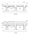
- FIG. 1 a schematically illustrates a top view of a semiconductor device 100 according to a complex design.
- the device 100 or its design comprises an active region 102 A, which is to be understood as a semiconductor region in which one or more transistors are to be formed.
- the active region 102 A is illustrated to comprise three transistors 150 A including respective gate electrode structures 130 A.
- the gate electrode structures 130 A may include a complex material system including a high-k dielectric material and a metal-containing electrode material, as discussed above.
- the gate electrode structures 130 A represent conductive lines extending across the active region 102 A and are typically formed with an end portion thereof on an isolation region 102 C, which laterally delineates the active region 102 A and any other active regions (not shown).
- a gate electrode structure 130 C may also extend above the isolation region 102 C in close proximity to the active region 102 A. It should be appreciated that a length of the gate electrode structures 130 A, 130 C may be 50 nm and less in sophisticated applications so that the distance between the gate electrode structure 130 C and the active region 102 A may be significantly less than the critical gate length.
- the transistors 150 A may represent devices that require the incorporation of a strain-inducing semiconductor material, such as a silicon/germanium alloy, possibly in combination with a semiconductor alloy for appropriately adjusting the threshold voltage of the transistors 150 A.
- FIG. 1 b schematically illustrates a cross-sectional view of a semiconductor device 100 according to the section indicated as Ib in FIG. 1 a .
- the device 100 comprises a substrate 101 and a semiconductor layer 102 , which is typically provided in the form of a silicon material.
- the substrate 101 and the semiconductor layer 102 may form a silicon-on-insulator (SOI) architecture when a buried insulating material (not shown) is formed below the semiconductor layer 102 .
- SOI silicon-on-insulator
- a bulk configuration may be formed by the semiconductor layer 102 and the substrate 101 , when the semiconductor layer 102 is a portion of a crystalline semiconductor material of the substrate 101 .
- the semiconductor layer 102 typically comprises a plurality of active regions, such as the active region 102 A, which are laterally delineated by the isolation region 102 C.
- the isolation region 102 C is typically comprised of silicon dioxide and may have a pronounced recessing 102 R that is positioned close to the active region 102 A.
- the gate electrode structures 130 A, 130 C are formed on the active region 102 A and the isolation region 102 C, respectively, and comprise a material system 131 , which is to be understood as a gate dielectric material including a high-k dielectric material, such as hafnium oxide and the like, in combination with a conventional dielectric material, such as silicon oxynitride and the like.
- the material system 131 comprises a metal-containing cap or electrode material, such as titanium nitride, which may also include appropriate metal species in order to obtain the desired work function, as is also discussed above.
- the material system 131 typically comprises a plurality of individual material layers, wherein the specific number and composition of the various material layers depend on device and process requirements.
- the gate electrode structures 130 A, 130 C comprise a further electrode material 132 , for instance in the form of a silicon material, followed by a dielectric cap material 133 , such as a silicon nitride material, a silicon dioxide material, or a combination thereof and the like.
- a liner or spacer 134 for instance comprised of silicon nitride, is formed on the sidewalls of the materials 132 and 131 in order that, in particular, any sensitive materials in the system 131 are appropriately protected.
- FIG. 1 c schematically illustrates a cross-sectional view along the section Ic of FIG. 1 a .
- the gate electrode structure 130 A is formed above the active region 102 A and extends with an end portion thereof into the isolation region 102 C. Also in this area, the pronounced recess 102 R is typically present and may have a significant influence on the final characteristics of the gate electrode structure 130 A.
- the semiconductor device 100 as shown in FIGS. 1 b and 1 c is formed on the basis of the following process techniques.
- the isolation region 102 C is formed in the semiconductor layer 102 on the basis of well-established shallow trench isolation process techniques. Thereafter, appropriate masking regimes may be applied so as to incorporate a desired well dopant species in the various active regions, such as the active region 102 A, thereby adjusting the basic transistor characteristics, such as conductivity type, threshold voltage and the like.
- a plurality of cleaning processes may typically have to be applied which may result in a certain degree of material erosion in the isolation region 102 C, wherein additional rework processes of the lithography processes may even further contribute to unwanted material erosion.
- an additional semiconductor material (not shown) is frequently provided on the basis of selective epitaxial growth techniques, for instance for appropriately adjusting the threshold voltage of P-channel transistors, wherein the corresponding masking process in combination with the selective epitaxial growth techniques and the surface preparation processes associated therewith may result in a pronounced material loss in the isolation region 102 C, in particular in the vicinity of the active region 102 A when corresponding to a P-channel transistor.
- the further processing is continued by providing material layers for the system 131 , possibly in combination with additional heat treatments so as to diffuse a work function adjusting metal species and the like.
- the material 132 and the cap material 133 are deposited on the basis of appropriate process techniques. It should be appreciated that providing appropriate work function metals for P-channel transistors and N-channel transistors, respectively, may also involve respective patterning processes.
- the complex layer stack is patterned by using sophisticated lithography and etch techniques followed by the deposition of a spacer layer or liner, which is subsequently patterned into the liner or spacer structure 134 .
- the spacer or liner material may be patterned in a later manufacturing stage, while in other cases a dedicated liner material may be formed and patterned prior to depositing the spacer material which may be used for forming the structure 134 .
- FIGS. 1 d - 1 f a process sequence will be described as an example for illustrating a failure mechanism, in which the encapsulation of the gate electrode structures, such as the gate electrode structure 130 C ( FIG. 1 b ), may be insufficient and may result in pronounced yield loss. It should be appreciated, however, that a similar exposure of sensitive gate materials may also occur at the end portions of the gate electrode structure 130 A caused by the pronounced recessing 102 R, as shown in FIG. 1 c.
- FIG. 1 d schematically illustrates the device 100 during an etch process 103 for forming cavities 103 A in the active region 102 A adjacent to the isolation region 102 C.
- the cap materials 133 and the liner 134 may act as an etch mask.
- FIG. 1 e schematically illustrates the device 100 during a cleaning process 104 in order to remove any etch byproducts and other contaminants, thereby, however, also contributing to a certain material erosion at exposed sidewall surface areas in the cavities 103 A.
- FIG. 1 f schematically illustrates the semiconductor device 100 during a further cleaning process 106 , which is typically performed prior to starting a selective epitaxial growth process in order to remove native oxides and the like.
- a certain degree of material erosion may occur in the cavities 103 A so that a sidewall surface area 131 S of the sensitive material system 131 may be exposed below the sidewall spacer structure 134 of the gate electrode structure 130 C. Consequently, sensitive materials may be attacked and may be removed, depending on the cleaning or etch chemistry used.
- the sidewalls may not be efficiently covered, thereby even further contributing to material deterioration of the system 131 during the further processing.
- the recessed configuration of the isolation region 102 C at or near the end portions of the gate electrode structure 130 A may also result in an exposure of any sensitive materials, thereby causing a significant shift of the overall material characteristics.
- the present disclosure relates to manufacturing techniques and semiconductor devices in which sophisticated high-k metal gate electrode structures may be formed in an early manufacturing stage, while avoiding or at least reducing the effects of one or more of the problems identified above.
- the present disclosure provides manufacturing techniques and semiconductor devices in which integrity of sensitive gate materials may be ensured with superior efficiency by reducing the degree of recessing of trench isolation regions in the vicinity of active regions. It has been recognized that, in particular, the recessed configuration of trench isolation regions in close proximity to active regions may significantly contribute to yield losses caused by gate failures or gate deterioration. According to the principles disclosed herein, a superior surface topography in isolation regions may be accomplished by providing an appropriate dielectric cap layer, which may result in superior resistivity with respect to a plurality of cleaning recipes, thereby significantly reducing undue material erosion prior to and during the complex manufacturing process for forming high-k metal gate electrode structures.
- the encapsulation of the sensitive gate material may be preserved during the further processing, for instance upon forming the strain-inducing semiconductor alloy, at least for one type of transistor.
- the superior etch resistivity of the trench isolation region may also be used in generally improving the overall surface topography, for instance, any differences in height level between active regions of P-channel transistors and N-channel transistors, which may typically be created during the process sequence for selectively forming a threshold adjusting semiconductor alloy.
- an appropriate adaptation of the height level of one type of active region may be applied without significantly affecting the surface topography of the trench isolation region in the vicinity of this active region due to the presence of the dielectric cap layer having the superior etch resistivity.
- One illustrative method disclosed herein comprises forming a trench isolation region in a semiconductor layer of a semiconductor device by using a first dielectric fill material, wherein the trench isolation region laterally delineates an active region in the semiconductor layer.
- the method further comprises forming a cap layer on the first dielectric material by using a second dielectric material, wherein the first and second dielectric materials have a different material composition.
- the method comprises forming a gate electrode structure on the active region and the trench isolation region, which includes the cap layer.
- a further illustrative method disclosed herein comprises forming a trench isolation region in a semiconductor layer of a semiconductor device by recessing a first dielectric material of the trench isolation region and by forming a second dielectric material as a cap layer on the recessed first dielectric material.
- the method further comprises forming a gate electrode structure on the cap layer of the trench isolation region, wherein the gate electrode structure comprises a high-k dielectric material.
- One illustrative semiconductor device disclosed herein comprises a trench isolation region that laterally delineates an active region in a semiconductor layer.
- the trench isolation region comprises a first dielectric material and a second dielectric material formed on the first dielectric material, wherein the first and second dielectric materials differ in their material composition.
- the semiconductor device further comprises a gate electrode structure formed on a channel area of the active region, wherein the gate electrode structure comprises a material system comprising a high-k dielectric material and a metal-containing electrode material.
- the gate electrode structure further comprises a protective liner formed on sidewalls of the high-k dielectric material and the metal-containing electrode material.
- FIG. 1 a schematically illustrates a top view of a semiconductor device comprising high-k metal gate electrode structures formed on the basis of a conventional process strategy
- FIGS. 1 b - 1 c schematically illustrate cross-sectional views of the device of FIG. 1 a;
- FIGS. 1 d - 1 f schematically illustrate cross-sectional views of a conventional manufacturing sequence for forming an embedded strain-inducing semiconductor alloy, thereby causing significant gate failures, according to conventional strategies;
- FIGS. 2 a - 2 j schematically illustrate cross-sectional views of a semiconductor device during various manufacturing stages in forming high-k metal gate electrode structures on the basis of trench isolation regions having a superior surface topography by providing an additional dielectric cap layer, according to illustrative embodiments.
- the present disclosure generally addresses the problem of gate failures, which may occur in conventional strategies by forming high-k metal gate electrode structures in an early manufacturing stage.
- the surface topography of the trench isolation regions is significantly enhanced by providing an appropriate dielectric cap layer, which exhibits a significantly increased robustness with respect to a plurality of etch chemistries, such as reactive wet chemical cleaning recipes and the like, thereby significantly reducing or substantially avoiding undue material removal, in particular prior to the complex processes required, for example, for the provision of a threshold adjusting semiconductor alloy and the like.
- the encapsulation of the sensitive gate materials may be preserved upon performing further complex manufacturing processes, such as the incorporation of a strain-inducing semiconductor material, the adaptation of height levels of active regions of P-channel transistors and N-channel transistors and the like.
- any gate failures caused by the presence of pronounced recessed areas of the trench isolation region adjacent to active regions may be significantly reduced, which thus contributes to superior production yield in a manufacturing process in which high-k metal gate electrode structures may be formed in an early manufacturing stage.
- FIGS. 2 a - 2 j further illustrative embodiments will now be described in more detail, wherein reference may also be made to FIGS. 1 a - 1 f.
- FIG. 2 a schematically illustrates a cross-sectional view of a semiconductor device 200 in an early manufacturing stage.
- the device 200 may comprise a substrate 201 , such as a semiconductor material or any other carrier material that is appropriate for forming thereon or thereabove a semiconductor layer 202 .
- the substrate 201 and the semiconductor layer 202 may form an SOI configuration when a buried insulating material (not shown) may be provided below the semiconductor layer 202 , while, in other cases, the semiconductor layer 202 may directly connect to a crystalline semiconductor material of the substrate 201 when a bulk configuration is considered.
- a hard mask layer 210 is formed above the semiconductor layer 202 and, in the embodiment shown, may comprise a first mask layer 210 A, such as a silicon dioxide layer, followed by a second mask layer 210 B, for instance provided in the form of a silicon nitride material.
- the layers 210 A, 210 B may be formed on the basis of any well-established process technique, for instance, by oxidation for the layer 210 A, or deposition using thermally activated chemical vapor deposition (CVD) and the like.
- the layer 210 B may be deposited by any appropriate deposition technique.
- the first mask layer 210 A may be provided with a thickness of approximately 10-25 nm so as to provide sufficient process margins during the further processing when forming a dielectric cap layer in trench isolation regions. Furthermore, the layer 210 B may be provided with a thickness of approximately 60-100 nm, depending on the overall device requirements. Thus, it should be appreciated that the thickness 210 T of the first mask layer 210 A is typically greater than an oxide layer of semiconductor devices that may receive a conventional trench isolation region, as is, for instance, described above with reference to the semiconductor device 100 .
- FIG. 2 b schematically illustrates the device 200 in a further advanced manufacturing stage in which trenches 202 T are formed so as to extend through the semiconductor layer 202 , thereby laterally delineating a plurality of active regions, such as active regions 202 A, 202 B.
- the mask layer 210 may be appropriately patterned on the basis of a lithography process using a resist material in order to pattern the mask layer 210 , which may then be used as a hard mask for etching into the semiconductor layer 202 .
- any well-established anisotropic etch techniques may be applied, as are also used in conventional strategies.
- FIG. 2 c schematically illustrates the device 200 with a first dielectric material 211 formed within the trenches 202 T and above the mask layer 210 .
- the material 211 may be formed on the basis of any appropriate technique, for instance by forming or depositing a liner material, such as a silicon dioxide liner material, which may be accomplished by oxidation and/or deposition using thermally activated CVD techniques and the like. Thereafter, a further silicon dioxide material may be deposited by applying high density plasma deposition recipes, thereby substantially void-free filling the trenches 202 T.
- a liner material such as a silicon dioxide liner material
- FIG. 2 d schematically illustrates the device 200 during a material removal process 205 , which may be applied as a chemical mechanical planarization or polishing process using appropriate etch recipes for removing a silicon dioxide material selectively with respect to the mask layer 210 B. Consequently, similarly as in conventional STI (shallow trench isolation) process techniques, the silicon nitride material of the layer 210 B may be used as a CMP stop material.
- a material removal process 205 may be applied as a chemical mechanical planarization or polishing process using appropriate etch recipes for removing a silicon dioxide material selectively with respect to the mask layer 210 B. Consequently, similarly as in conventional STI (shallow trench isolation) process techniques, the silicon nitride material of the layer 210 B may be used as a CMP stop material.
- FIG. 2 e schematically illustrates the device 200 when exposed to a reactive etch atmosphere 208 , which may be selected such that the material 211 may be preferably removed with respect to the mask material 210 B and also selectively with respect to the material of the active regions 202 A, 202 B.
- a reactive etch atmosphere 208 which may be selected such that the material 211 may be preferably removed with respect to the mask material 210 B and also selectively with respect to the material of the active regions 202 A, 202 B.
- a plurality of highly selective etch recipes are available, for instance based on hydrofluoric acid (HF) and the like. It should be appreciated that a certain degree of “under etching” of the layer 210 B, for instance by removing material of the layer 210 A, may be less critical since a corresponding material erosion in the layer 210 A may be efficiently compensated for during the further processing.
- a desired degree of recessing, indicated as 211 R, of a surface 211 S of the dielectric material 211 with respect to a surface 202 S of the active regions 202 A, 202 B may be adjusted.
- the degree of recessing 211 R may be adjusted to approximately 5-50 nm, depending on the etch resistivity of a further dielectric material to be filled into the trench 202 T in a later manufacturing stage.
- FIG. 2 f schematically illustrates the semiconductor device 200 with a second dielectric material 212 formed above the mask layer 210 B and on the first dielectric material 211 , thereby refilling the isolation trenches 202 T.
- the dielectric material 212 may be provided in the form of a silicon and nitrogen-containing dielectric material which may be deposited on the basis of high density plasma CVD or on the basis of low pressure CVD using well-established deposition recipes for silicon nitride material.
- the dielectric material 211 Prior to or after the deposition of the material 212 , the dielectric material 211 may be densified by performing an anneal process, for instance after the deposition of the material 211 ( FIG.
- the materials 211 and 212 in combination, reliably fill the isolation trenches 202 T and provide the required dielectric and mechanical characteristics, while additionally the material 212 may provide superior etch resistivity with respect to a plurality of wet chemical etch chemistries, such as hydrofluoric acid and the like.
- the material 212 may be provided in the form of any other dielectric material having a high etch selectivity with respect to the silicon dioxide material, i.e., the material 211 , amorphous carbon material may be deposited on the basis of well-established CVD techniques.
- FIG. 2 g schematically illustrates the device 200 during a further material removal process 209 , such as a planarization process using well-established process recipes for, for instance, removing silicon nitride material, wherein the layer 210 A may be used as a stop material.
- the removal process 209 may be controlled on the basis of appropriately selecting the polish time in order to substantially expose the layer 210 A.
- the mask layer 210 FIG. 2 a
- a layer thickness of 2-10 nm may be selected for a corresponding stop layer, which may then be used for more efficiently controlling the removal process 209 .
- hafnium oxide is a well-established material which may also be used as an efficient high-k dielectric material during the further processing of the device 200 .
- FIG. 2 h schematically illustrates the device 200 during a further etch process 213 in which the height level of trench isolation regions 202 C, comprised of the materials 211 and 212 , may be reduced as, for instance, indicated by 212 R, which may be accomplished on the basis of any appropriate etch chemistry, such as a mixture of hydrofluoric acid and ethylene glycol (HFEG) or based on any other appropriate etch chemistry, which exhibits a high degree of selectivity with respect to silicon material.
- the height level may be reduced without affecting the active regions 202 A, 202 B.
- the material of the layer 210 A may also be removed to a certain degree, depending on the selectivity of the etch chemistry of the process 213 .
- any further control material such as hafnium oxide and the like, may be removed prior to, during or after the process 213 , while using the remaining portion of the mask layer 210 A as an appropriate etch protection layer.
- FIG. 2 i schematically illustrates the device 200 after the removal of the mask layer 210 A ( FIG. 2 h ).
- the removal may be accomplished by using well-established wet chemical etch recipes, for instance by applying HF, wherein the cap layer 212 in the isolation regions 202 C may substantially preserve the previously established surface topography thereof.
- the further processing may be continued on the basis of the isolation regions 202 C having the desired surface topography, wherein the dielectric cap layer 212 may provide superior robustness during any cleaning recipes, which typically include reactive agents that may efficiently remove any silicon oxide-based materials.
- a threshold adjusting semiconductor material may be selectively formed on one type of active region, for instance in the active region 202 A, while other active regions, such as the active region 202 B, may be appropriately covered.
- well-established masking regimes and selective epitaxial growth techniques in combination with appropriate cleaning recipes may be applied, wherein the dielectric cap layer 212 may significantly reduce undue recessing of any non-masked areas of the isolation regions 202 C.
- a selective removal of material of the cap layers 212 in previously masked areas may be applied by using a resist mask and applying an appropriate etch chemistry for removing a portion of the dielectric cap layer 212 .
- a difference in height levels of the active region 202 A, which may receive the threshold adjusting semiconductor alloy, and the active region 202 B, which may not receive a corresponding semiconductor alloy may be accomplished by recessing the active region 202 A and re-growing the semiconductor alloy within the recess, wherein the degree of recessing and/or the thickness of the semiconductor alloy may be appropriately selected so as to obtain a desired height level.
- a strain-inducing semiconductor alloy may be formed, wherein also the superior robustness of the dielectric cap layer 212 may significantly reduce the probability of exposing sensitive gate materials.
- FIG. 2 j schematically illustrates the semiconductor device 200 in a further advanced manufacturing stage.
- gate electrode structures 230 A of transistors 250 A may be formed on the active region 202 A and gate electrode structures 230 B of transistors 250 B may be formed on the active region 202 B.
- the gate electrode structures 230 A, 230 B may also extend with respective end portions above the isolation region 202 C, depending on the overall layout requirements.
- a gate electrode structure 230 C may be formed on the isolation region 202 C in close proximity to the active region 202 A.
- the gate electrode structures 230 A, 230 B, 230 C may comprise a material system 231 acting as a gate insulation layer and may comprise a high-k dielectric material 231 B, possibly in combination with a conventional gate dielectric material 231 A, such as silicon dioxide, silicon oxynitride and the like.
- a metal-containing electrode material 232 A may be formed on the gate insulation layer 231 and may be comprised of titanium nitride, tantalum, tantalum nitride and the like.
- a semiconductor-based electrode material 232 may be provided.
- the materials 232 , 232 A and the gate insulation layer 231 may be encapsulated by a liner or sidewall spacer 234 and a dielectric cap layer 233 may be provided.
- the gate electrode structures 230 A may differ from the gate electrode structures 230 B with respect to a work function adjusting metal species and the like, when the transistors 250 A, 250 B represent different types of transistors, such as P-channel transistors and N-channel transistors, respectively.
- the gate electrode structures 230 A, 230 B, 230 C may be provided with a gate length of 50 nm and less in sophisticated applications.
- a threshold voltage adjusting semiconductor alloy such as a silicon/germanium alloy 251 A may be provided so as to act as a portion of a channel area 251 , which thus forms an interface 251 S with the corresponding gate insulation layers 231 . Consequently, as discussed above, due to the presence of the dielectric cap layer 212 in the isolation regions 202 C, in addition to a superior surface topography of the isolation regions 202 C, a height level of the dielectric material 211 may be less than a height level defined by the interface 251 S, as is indicated by the difference in height levels 251 D.
- cavities 203 A may be filled or overfilled with an appropriate strain-inducing semiconductor material 253 , such as a silicon/germanium alloy, a silicon/tin alloy, a silicon/germanium/tin alloy, a silicon/carbon alloy and the like.
- an appropriate strain-inducing semiconductor material 253 such as a silicon/germanium alloy, a silicon/tin alloy, a silicon/germanium/tin alloy, a silicon/carbon alloy and the like.
- the materials 253 and 251 A may not be present in the active region 202 B, depending on the overall device requirements.
- the semiconductor device 200 as shown in FIG. 2 j may be formed on the basis of process techniques described above and also described with reference to the semiconductor device 100 . That is, after forming the isolation regions 202 C having the superior surface topography due to the dielectric cap layer 212 , the further processing may be continued by incorporating appropriate well dopant species into the active regions 202 A, 202 B, wherein additional rework processes may not negatively affect the finally obtained surface topography of the regions 202 C. Thereafter, if required, the material 251 A may be incorporated into the active region 202 A, while the active region 202 B may be masked, for instance, by an oxide hard mask material and the like.
- the region 202 A may be recessed prior to growing the material 251 A in order to obtain a desired surface leveling with respect to the active region 202 B.
- the gate electrode structures 230 A, 230 B, 230 C may be formed on the basis of process techniques as described above with reference to the device 100 .
- the liner or spacer 234 may be formed so as to reliably confine the sensitive gate materials 231 , 232 A. Due to the robustness of the dielectric cap layer 212 , pronounced recess portions, such as the portions 102 R (see FIGS. 1 b - 1 f ), may be avoided or at least significantly reduced, thereby also increasing integrity of the liner 234 and thus of the sensitive materials 231 , 232 A.
- the present disclosure provides manufacturing techniques and semiconductor devices in which the encapsulation of sophisticated high-k metal gate electrode structures may be improved by reducing the surface topography of trench isolation regions.
- this material is recessed and an appropriate second dielectric material is provided, which has higher etch resistivity with respect to a plurality of cleaning recipes.
- increased production yield may be obtained for process techniques in which high-k metal gate electrode structures are to be provided in an early manufacturing stage.
Abstract
Description
Claims (22)
Applications Claiming Priority (3)
| Application Number | Priority Date | Filing Date | Title |
|---|---|---|---|
| DE102011004922 | 2011-03-01 | ||
| DE102011004922.3A DE102011004922B4 (en) | 2011-03-01 | 2011-03-01 | Method of fabricating transistors with metal gate stacks with increased integrity |
| DE102011004922.3 | 2011-03-01 |
Publications (2)
| Publication Number | Publication Date |
|---|---|
| US20120223407A1 US20120223407A1 (en) | 2012-09-06 |
| US8916433B2 true US8916433B2 (en) | 2014-12-23 |
Family
ID=46671234
Family Applications (1)
| Application Number | Title | Priority Date | Filing Date |
|---|---|---|---|
| US13/406,869 Active 2032-07-17 US8916433B2 (en) | 2011-03-01 | 2012-02-28 | Superior integrity of high-k metal gate stacks by capping STI regions |
Country Status (6)
| Country | Link |
|---|---|
| US (1) | US8916433B2 (en) |
| KR (1) | KR101396519B1 (en) |
| CN (1) | CN102683261B (en) |
| DE (1) | DE102011004922B4 (en) |
| SG (2) | SG10201405133YA (en) |
| TW (1) | TWI506726B (en) |
Cited By (3)
| Publication number | Priority date | Publication date | Assignee | Title |
|---|---|---|---|---|
| US10916515B2 (en) | 2014-10-22 | 2021-02-09 | Infineon Technologies Ag | Systems and methods using an RF circuit on isolating material |
| US11728173B2 (en) | 2020-09-30 | 2023-08-15 | Taiwan Semiconductor Manufacturing Co., Ltd. | Masking layer with post treatment |
| US11758713B2 (en) | 2020-12-15 | 2023-09-12 | Samsung Electronics Co., Ltd. | Semiconductor devices |
Families Citing this family (5)
| Publication number | Priority date | Publication date | Assignee | Title |
|---|---|---|---|---|
| US9469522B2 (en) | 2013-03-15 | 2016-10-18 | Robert Bosch Gmbh | Epi-poly etch stop for out of plane spacer defined electrode |
| US9502418B2 (en) | 2014-10-02 | 2016-11-22 | International Business Machines Corporation | Semiconductor devices with sidewall spacers of equal thickness |
| CN106486377B (en) * | 2015-09-01 | 2019-11-29 | 中芯国际集成电路制造(上海)有限公司 | Fin type semiconductor devices and its manufacturing method |
| US10535550B2 (en) * | 2017-08-28 | 2020-01-14 | International Business Machines Corporation | Protection of low temperature isolation fill |
| US11170992B2 (en) | 2018-04-27 | 2021-11-09 | Tokyo Electron Limited | Area selective deposition for cap layer formation in advanced contacts |
Citations (9)
| Publication number | Priority date | Publication date | Assignee | Title |
|---|---|---|---|---|
| US6204185B1 (en) * | 1999-05-24 | 2001-03-20 | United Microelectronics Corp. | Method for forming self-align stop layer for borderless contact process |
| US20010031540A1 (en) * | 1999-07-12 | 2001-10-18 | Chartered Semiconductor Manufacturing Ltd. | Silicon nitride capped shallow trench isolation method for fabricating sub-micron devices with borderless contacts |
| US6403482B1 (en) * | 2000-06-28 | 2002-06-11 | International Business Machines Corporation | Self-aligned junction isolation |
| US6586814B1 (en) * | 2000-12-11 | 2003-07-01 | Lsi Logic Corporation | Etch resistant shallow trench isolation in a semiconductor wafer |
| US6653194B1 (en) * | 2002-05-07 | 2003-11-25 | Hynix Semiconductor Inc. | Method for forming contact hole in semiconductor device |
| US20060278952A1 (en) * | 2005-06-14 | 2006-12-14 | Fujitsu Limited | Semiconductor device and fabrication process thereof |
| US20090011584A1 (en) * | 2006-07-03 | 2009-01-08 | Hynix Semiconductor Inc. | Method for forming transistor of semiconductor device |
| DE102009021489A1 (en) | 2009-05-15 | 2010-11-18 | Globalfoundries Dresden Module One Llc & Co. Kg | Increasing the deposition uniformity for a semiconductor alloy by an in-situ etching process |
| US8026151B2 (en) * | 2006-05-26 | 2011-09-27 | Semiconductor Manufacturing International (Shanghai) Corporation | Method with high gapfill capability for semiconductor devices |
Family Cites Families (8)
| Publication number | Priority date | Publication date | Assignee | Title |
|---|---|---|---|---|
| US6037238A (en) * | 1999-01-04 | 2000-03-14 | Vanguard International Semiconductor Corporation | Process to reduce defect formation occurring during shallow trench isolation formation |
| JP4756926B2 (en) * | 2005-06-17 | 2011-08-24 | Okiセミコンダクタ株式会社 | Method for manufacturing element isolation structure |
| US7763534B2 (en) * | 2007-10-26 | 2010-07-27 | Tela Innovations, Inc. | Methods, structures and designs for self-aligning local interconnects used in integrated circuits |
| CN101154615A (en) * | 2006-09-25 | 2008-04-02 | 上海华虹Nec电子有限公司 | Method for forming insulated isolation at source-drain bottom |
| KR100821089B1 (en) * | 2006-12-27 | 2008-04-08 | 동부일렉트로닉스 주식회사 | Semiconductor device and method for fabricating the same |
| JP5141029B2 (en) * | 2007-02-07 | 2013-02-13 | 富士通セミコンダクター株式会社 | Semiconductor device and manufacturing method thereof |
| JP2009212450A (en) * | 2008-03-06 | 2009-09-17 | Toshiba Corp | Semiconductor device and manufacturing method of semiconductor device |
| JP2009290069A (en) * | 2008-05-30 | 2009-12-10 | Renesas Technology Corp | Semiconductor device, and method of manufacturing the same |
-
2011
- 2011-03-01 DE DE102011004922.3A patent/DE102011004922B4/en not_active Expired - Fee Related
-
2012
- 2012-02-17 SG SG10201405133YA patent/SG10201405133YA/en unknown
- 2012-02-17 SG SG2012011326A patent/SG183635A1/en unknown
- 2012-02-17 TW TW101105209A patent/TWI506726B/en not_active IP Right Cessation
- 2012-02-27 CN CN201210048312.0A patent/CN102683261B/en not_active Expired - Fee Related
- 2012-02-28 US US13/406,869 patent/US8916433B2/en active Active
- 2012-02-29 KR KR1020120021389A patent/KR101396519B1/en not_active IP Right Cessation
Patent Citations (11)
| Publication number | Priority date | Publication date | Assignee | Title |
|---|---|---|---|---|
| US6204185B1 (en) * | 1999-05-24 | 2001-03-20 | United Microelectronics Corp. | Method for forming self-align stop layer for borderless contact process |
| US20010031540A1 (en) * | 1999-07-12 | 2001-10-18 | Chartered Semiconductor Manufacturing Ltd. | Silicon nitride capped shallow trench isolation method for fabricating sub-micron devices with borderless contacts |
| US6350661B2 (en) * | 1999-07-12 | 2002-02-26 | Chartered Semiconductor Manufacturing Ltd. | Silicon nitride capped shallow trench isolation method for fabricating sub-micron devices with borderless contacts |
| US6403482B1 (en) * | 2000-06-28 | 2002-06-11 | International Business Machines Corporation | Self-aligned junction isolation |
| US6586814B1 (en) * | 2000-12-11 | 2003-07-01 | Lsi Logic Corporation | Etch resistant shallow trench isolation in a semiconductor wafer |
| US6653194B1 (en) * | 2002-05-07 | 2003-11-25 | Hynix Semiconductor Inc. | Method for forming contact hole in semiconductor device |
| US20060278952A1 (en) * | 2005-06-14 | 2006-12-14 | Fujitsu Limited | Semiconductor device and fabrication process thereof |
| US8026151B2 (en) * | 2006-05-26 | 2011-09-27 | Semiconductor Manufacturing International (Shanghai) Corporation | Method with high gapfill capability for semiconductor devices |
| US20090011584A1 (en) * | 2006-07-03 | 2009-01-08 | Hynix Semiconductor Inc. | Method for forming transistor of semiconductor device |
| DE102009021489A1 (en) | 2009-05-15 | 2010-11-18 | Globalfoundries Dresden Module One Llc & Co. Kg | Increasing the deposition uniformity for a semiconductor alloy by an in-situ etching process |
| US20100289094A1 (en) | 2009-05-15 | 2010-11-18 | Carsten Reichel | Enhancing deposition uniformity of a channel semiconductor alloy by an in situ etch process |
Non-Patent Citations (1)
| Title |
|---|
| Translation of Official Communication from German Patent Office for German Patent Application No. 10 2011 004 922.3 dated Jan. 9, 2012. |
Cited By (3)
| Publication number | Priority date | Publication date | Assignee | Title |
|---|---|---|---|---|
| US10916515B2 (en) | 2014-10-22 | 2021-02-09 | Infineon Technologies Ag | Systems and methods using an RF circuit on isolating material |
| US11728173B2 (en) | 2020-09-30 | 2023-08-15 | Taiwan Semiconductor Manufacturing Co., Ltd. | Masking layer with post treatment |
| US11758713B2 (en) | 2020-12-15 | 2023-09-12 | Samsung Electronics Co., Ltd. | Semiconductor devices |
Also Published As
| Publication number | Publication date |
|---|---|
| KR101396519B1 (en) | 2014-05-22 |
| SG183635A1 (en) | 2012-09-27 |
| US20120223407A1 (en) | 2012-09-06 |
| TWI506726B (en) | 2015-11-01 |
| SG10201405133YA (en) | 2014-10-30 |
| CN102683261A (en) | 2012-09-19 |
| DE102011004922B4 (en) | 2016-12-15 |
| CN102683261B (en) | 2015-09-02 |
| DE102011004922A1 (en) | 2012-09-06 |
| KR20120099598A (en) | 2012-09-11 |
| TW201246449A (en) | 2012-11-16 |
Similar Documents
| Publication | Publication Date | Title |
|---|---|---|
| US8916433B2 (en) | Superior integrity of high-k metal gate stacks by capping STI regions | |
| US9425280B2 (en) | Semiconductor device with low-K spacers | |
| US8367495B2 (en) | Method for forming CMOS transistors having metal-containing gate electrodes formed on a high-K gate dielectric material | |
| US8617940B2 (en) | SOI device with a buried insulating material having increased etch resistivity | |
| US8716120B2 (en) | High-k metal gate electrode structures formed by reducing a gate fill aspect ratio in replacement gate technology | |
| US8748275B2 (en) | Semiconductor devices comprising a channel semiconductor alloy formed with reduced STI topography | |
| US8329549B2 (en) | Enhancing integrity of a high-k gate stack by protecting a liner at the gate bottom during gate head exposure | |
| US8324119B2 (en) | Enhancing deposition uniformity of a channel semiconductor alloy by an in situ etch process | |
| US8409942B2 (en) | Replacement gate approach based on a reverse offset spacer applied prior to work function metal deposition | |
| US8378432B2 (en) | Maintaining integrity of a high-K gate stack by an offset spacer used to determine an offset of a strain-inducing semiconductor alloy | |
| US7981740B2 (en) | Enhanced cap layer integrity in a high-K metal gate stack by using a hard mask for offset spacer patterning | |
| US8334573B2 (en) | Buried etch stop layer in trench isolation structures for superior surface planarity in densely packed semiconductor devices | |
| US8383500B2 (en) | Semiconductor device formed by a replacement gate approach based on an early work function metal | |
| US8658509B2 (en) | Semiconductor resistors formed at a lower height level in a semiconductor device comprising metal gates | |
| US8349694B2 (en) | Enhanced confinement of high-K metal gate electrode structures by reducing material erosion of a dielectric cap layer upon forming a strain-inducing semiconductor alloy | |
| US8198152B2 (en) | Transistors comprising high-k metal gate electrode structures and adapted channel semiconductor materials | |
| US20120001263A1 (en) | Replacement Gate Approach for High-K Metal Gate Stacks Based on a Non-Conformal Interlayer Dielectric | |
| US8486786B2 (en) | Enhancing uniformity of a channel semiconductor alloy by forming STI structures after the growth process | |
| US8173501B2 (en) | Reduced STI topography in high-K metal gate transistors by using a mask after channel semiconductor alloy deposition | |
| US8623742B2 (en) | Reduced STI loss for superior surface planarity of embedded stressors in densely packed semiconductor devices | |
| US20120235245A1 (en) | Superior integrity of high-k metal gate stacks by reducing sti divots by depositing a fill material after sti formation | |
| US8609509B2 (en) | Superior integrity of high-k metal gate stacks by forming STI regions after gate metals | |
| US8481381B2 (en) | Superior integrity of high-k metal gate stacks by preserving a resist material above end caps of gate electrode structures | |
| US20110266625A1 (en) | Maintaining Integrity of a High-K Gate Stack After Embedding a Stressor Material by Using a Liner | |
| US8143132B2 (en) | Transistor including a high-K metal gate electrode structure formed on the basis of a simplified spacer regime |
Legal Events
| Date | Code | Title | Description |
|---|---|---|---|
| AS | Assignment |
Owner name: GLOBALFOUNDRIES INC., CAYMAN ISLANDS Free format text: ASSIGNMENT OF ASSIGNORS INTEREST;ASSIGNORS:SCHEIPER, THILO;BAARS, PETER;BEYER, SVEN;SIGNING DATES FROM 20110615 TO 20110620;REEL/FRAME:027774/0474 |
|
| STCF | Information on status: patent grant |
Free format text: PATENTED CASE |
|
| MAFP | Maintenance fee payment |
Free format text: PAYMENT OF MAINTENANCE FEE, 4TH YEAR, LARGE ENTITY (ORIGINAL EVENT CODE: M1551) Year of fee payment: 4 |
|
| AS | Assignment |
Owner name: WILMINGTON TRUST, NATIONAL ASSOCIATION, DELAWARE Free format text: SECURITY AGREEMENT;ASSIGNOR:GLOBALFOUNDRIES INC.;REEL/FRAME:049490/0001 Effective date: 20181127 |
|
| AS | Assignment |
Owner name: GLOBALFOUNDRIES U.S. INC., CALIFORNIA Free format text: ASSIGNMENT OF ASSIGNORS INTEREST;ASSIGNOR:GLOBALFOUNDRIES INC.;REEL/FRAME:054633/0001 Effective date: 20201022 |
|
| AS | Assignment |
Owner name: GLOBALFOUNDRIES INC., CAYMAN ISLANDS Free format text: RELEASE BY SECURED PARTY;ASSIGNOR:WILMINGTON TRUST, NATIONAL ASSOCIATION;REEL/FRAME:054636/0001 Effective date: 20201117 |
|
| AS | Assignment |
Owner name: GLOBALFOUNDRIES U.S. INC., NEW YORK Free format text: RELEASE BY SECURED PARTY;ASSIGNOR:WILMINGTON TRUST, NATIONAL ASSOCIATION;REEL/FRAME:056987/0001 Effective date: 20201117 |
|
| MAFP | Maintenance fee payment |
Free format text: PAYMENT OF MAINTENANCE FEE, 8TH YEAR, LARGE ENTITY (ORIGINAL EVENT CODE: M1552); ENTITY STATUS OF PATENT OWNER: LARGE ENTITY Year of fee payment: 8 |