US8912014B1 - Controlling the latchup effect - Google Patents
Controlling the latchup effect Download PDFInfo
- Publication number
- US8912014B1 US8912014B1 US11/333,208 US33320806A US8912014B1 US 8912014 B1 US8912014 B1 US 8912014B1 US 33320806 A US33320806 A US 33320806A US 8912014 B1 US8912014 B1 US 8912014B1
- Authority
- US
- United States
- Prior art keywords
- source
- well contact
- tub
- region
- latchup
- Prior art date
- Legal status (The legal status is an assumption and is not a legal conclusion. Google has not performed a legal analysis and makes no representation as to the accuracy of the status listed.)
- Active, expires
Links
Images


Classifications
-
- G—PHYSICS
- G01—MEASURING; TESTING
- G01R—MEASURING ELECTRIC VARIABLES; MEASURING MAGNETIC VARIABLES
- G01R31/00—Arrangements for testing electric properties; Arrangements for locating electric faults; Arrangements for electrical testing characterised by what is being tested not provided for elsewhere
- G01R31/26—Testing of individual semiconductor devices
- G01R31/27—Testing of devices without physical removal from the circuit of which they form part, e.g. compensating for effects surrounding elements
-
- G—PHYSICS
- G01—MEASURING; TESTING
- G01R—MEASURING ELECTRIC VARIABLES; MEASURING MAGNETIC VARIABLES
- G01R31/00—Arrangements for testing electric properties; Arrangements for locating electric faults; Arrangements for electrical testing characterised by what is being tested not provided for elsewhere
- G01R31/28—Testing of electronic circuits, e.g. by signal tracer
- G01R31/2851—Testing of integrated circuits [IC]
- G01R31/2884—Testing of integrated circuits [IC] using dedicated test connectors, test elements or test circuits on the IC under test
-
- H—ELECTRICITY
- H10—SEMICONDUCTOR DEVICES; ELECTRIC SOLID-STATE DEVICES NOT OTHERWISE PROVIDED FOR
- H10P—GENERIC PROCESSES OR APPARATUS FOR THE MANUFACTURE OR TREATMENT OF DEVICES COVERED BY CLASS H10
- H10P74/00—Testing or measuring during manufacture or treatment of wafers, substrates or devices
- H10P74/20—Testing or measuring during manufacture or treatment of wafers, substrates or devices characterised by the properties tested or measured, e.g. structural or electrical properties
- H10P74/203—Structural properties, e.g. testing or measuring thicknesses, line widths, warpage, bond strengths or physical defects
-
- H—ELECTRICITY
- H10—SEMICONDUCTOR DEVICES; ELECTRIC SOLID-STATE DEVICES NOT OTHERWISE PROVIDED FOR
- H10P—GENERIC PROCESSES OR APPARATUS FOR THE MANUFACTURE OR TREATMENT OF DEVICES COVERED BY CLASS H10
- H10P74/00—Testing or measuring during manufacture or treatment of wafers, substrates or devices
- H10P74/27—Structural arrangements therefor
- H10P74/277—Circuits for electrically characterising or monitoring manufacturing processes, e.g. circuits in tested chips or circuits in testing wafers
-
- H—ELECTRICITY
- H10—SEMICONDUCTOR DEVICES; ELECTRIC SOLID-STATE DEVICES NOT OTHERWISE PROVIDED FOR
- H10D—INORGANIC ELECTRIC SEMICONDUCTOR DEVICES
- H10D84/00—Integrated devices formed in or on semiconductor substrates that comprise only semiconducting layers, e.g. on Si wafers or on GaAs-on-Si wafers
- H10D84/80—Integrated devices formed in or on semiconductor substrates that comprise only semiconducting layers, e.g. on Si wafers or on GaAs-on-Si wafers characterised by the integration of at least one component covered by groups H10D12/00 or H10D30/00, e.g. integration of IGFETs
- H10D84/82—Integrated devices formed in or on semiconductor substrates that comprise only semiconducting layers, e.g. on Si wafers or on GaAs-on-Si wafers characterised by the integration of at least one component covered by groups H10D12/00 or H10D30/00, e.g. integration of IGFETs of only field-effect components
- H10D84/83—Integrated devices formed in or on semiconductor substrates that comprise only semiconducting layers, e.g. on Si wafers or on GaAs-on-Si wafers characterised by the integration of at least one component covered by groups H10D12/00 or H10D30/00, e.g. integration of IGFETs of only field-effect components of only insulated-gate FETs [IGFET]
- H10D84/85—Complementary IGFETs, e.g. CMOS
- H10D84/854—Complementary IGFETs, e.g. CMOS comprising arrangements for preventing bipolar actions between the different IGFET regions, e.g. arrangements for latchup prevention
Definitions
- Implementations consistent with the principles of the invention relate generally to semiconductor devices and methods of manufacturing semiconductor devices.
- the invention has particular applicability to limiting the effect of latchup.
- the latchup effect creates a low resistance path between the positive and negative voltage supplies of a Complementary Metal Oxide Semiconductor (CMOS) circuit and enables the flow of large currents through the affected circuit.
- CMOS Complementary Metal Oxide Semiconductor
- a method in an implementation consistent with the principles of the invention, includes varying spacing between at least one of a source region or a drain region and a well contact region to create a group of configurations. The method further includes determining an effect of latchup on each configuration.
- a method in another implementation consistent with the principles of the invention, includes varying dimensions of at least one of a source region or a drain region and a well contact region to create a group of configurations.
- the group of configurations includes at least two of a first configuration where a length of the at least one of a source region or a drain region is greater than a length of the well contact region and a width of the at least one of a source region or a drain region is substantially similar to a width of the well contact region, a second configuration where a length of the at least one of a source region or a drain region is shorter than a length of the well contact region and a width of the at least one of a source region or a drain region is substantially similar to a width of the well contact region, a third configuration where a length and a width of the at least one of a source region or a drain region are greater than a length and a width of the well contact region, or a fourth configuration where a width of the at least one of a source region or
- a method in yet another implementation consistent with the principles of the invention, includes varying dimensions of at least one of a source region or a drain region and a well contact region and a distance between the at least one of a source region or a drain region and the well contact region to create a group of configurations. The method further includes determining an effect of latchup on each configuration in the group of configurations.
- FIGS. 1A and 1B illustrate exemplary views of a latchup monitor
- FIGS. 2-6B illustrate exemplary views for forming a latchup monitor in an implementation consistent with the principles of the invention
- FIGS. 7A-7B illustrate exemplary views for forming a latchup monitor in another implementation consistent with the principles of the invention
- FIGS. 8A-8B illustrate exemplary views for forming a latchup monitor in a further implementation consistent with the principles of the invention.
- FIGS. 9A-9B illustrate exemplary views for forming a latchup monitor in still another implementation consistent with the principles of the invention.
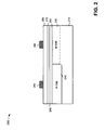
- FIGS. 1A and 1B illustrate exemplary views of a latchup monitor 100 .
- latchup monitor 100 is formed in a semiconductor memory device (e.g., a flash memory device).
- FIG. 1B illustrates a top view of a portion of latchup monitor 100 .
- FIG. 1A illustrates a cross section of latchup monitor 100 taken along line A-A in FIG. 1B .
- latchup monitor 100 may include a layer 110 , having wells 120 and 130 (also referred to herein as “tubs”) formed therein.
- layer 110 may include a lightly doped P over a heavily doped p+ substrate or P substrate
- tub 120 may include a p-tub (i.e., a tub doped with p-type impurities)
- tub 130 may include an n-tub (i.e., a tub doped with n-type impurities).
- FIG. 1A illustrates a twin tub design, it will be appreciated that, alternatively, a single p-tub or n-tub may be formed in an n-type substrate or p-type substrate, respectively.
- Source and drain regions 122 and a well region 124 may be formed in p-tub 120 .
- Source and drain regions 122 may be doped with n-type impurities, such as phosphorous or arsenic, and well region 124 may be doped with p-type impurities, such as boron.
- Source and drain regions 122 and well region 124 may be formed to a width of 0.3 ⁇ m or larger.
- source and drain regions 132 and a well region 134 may be formed in n-tub 130 .
- Source and drain regions 132 may be doped with p-type impurities, such as boron, and well region 134 may be doped with n-type impurities, such as phosphorous or arsenic.
- Source and drain regions 132 and well region 134 may be formed to a width of 0.3 ⁇ m or larger.
- Memory cells 140 may be formed on a top surface of p-tub 120 and n-tub 130 .
- Memory cells 140 may include a first dielectric layer 142 that acts as a tunnel oxide layer, a charge storage layer 144 , a second dielectric layer 146 that acts as an inter-gate dielectric, and a conductive layer 148 that may be used to form a control gate electrode.
- source/drain regions 122 and 132 and well regions 124 and 134 may be formed to a length of 10 ⁇ m.
- a distance between well region 124 and source/drain region 122 may range from 10 ⁇ m to 100 ⁇ m.
- a distance between source/drain region 122 and source/drain region 132 may range from 0.8 ⁇ m to 2 ⁇ m.
- a distance between source/drain region 132 and well region 134 may range from 10 ⁇ m to 100 ⁇ m.
- Latchup monitor 100 may be used to measure latchup associated with memory cells 140 .
- FIGS. 2-9B illustrate various latchup monitor configurations consistent with the principles of the invention. While the following description focuses on the formation of latchup monitors in semiconductor memory devices, it will be appreciated that the latchup monitor configurations described herein may alternatively be formed in other types of semiconductor devices that experience latchup, such as transistor devices.
- FIGS. 2-6B illustrate exemplary views for forming a latchup monitor in a first implementation consistent with the principles of the invention. Processing may begin with a semiconductor device 200 , as illustrated in FIG. 2 , that includes layers 210 , 250 , 260 , 270 , and 280 .
- layer 210 may include a substrate of semiconductor device 200 and may include silicon, germanium, silicon-germanium or other semiconducting materials.
- layer 210 may be a conductive layer or a dielectric layer formed a number of layers above the surface of a substrate in semiconductor device 200 .
- layer 110 may include a lightly doped n-type (or p-type substrate) over a heavily doped n-type (or p-type) substrate or a p-substrate.
- tubs may be formed in layer 110 .
- two tubs 230 and 240 may be formed in layer 110 in a conventional manner.
- Tub 230 may, for example, include an n-tub (i.e., a tub doped with n-type impurities) and tub 240 may, for example, include a p-tub (i.e., a tub doped with p-type impurities).
- FIG. 2 illustrates a twin tub design, it will be appreciated that, in other implementations consistent with the principles of the invention, a single p-tub or n-tub may be formed in an n-type substrate or p-type substrate, respectively.
- Layer 250 may be a dielectric layer formed on layer 210 in a conventional manner.
- dielectric layer 250 may include an oxide, such as a silicon oxide (e.g., SiO 2 ), and may have a thickness ranging from about 20 ⁇ to about 120 ⁇ .
- Dielectric layer 250 may function as a tunnel oxide layer for a subsequently formed memory cell of semiconductor device 200 .
- Layer 260 may be formed on layer 250 in a conventional manner and may include a dielectric material, such as a nitride (e.g., a silicon nitride), an oxide, such as Al 2 O 3 or HfO 2 , etc. Layer 260 , consistent with the invention, may act as a charge storage layer for semiconductor device 200 and may have a thickness ranging from about 30 ⁇ to about 150 ⁇ . Alternatively, layer 260 may include a conductive material, such as polycrystalline silicon, used to form a floating gate electrode for semiconductor device 200 .
- a dielectric material such as a nitride (e.g., a silicon nitride), an oxide, such as Al 2 O 3 or HfO 2 , etc.
- Layer 260 may act as a charge storage layer for semiconductor device 200 and may have a thickness ranging from about 30 ⁇ to about 150 ⁇ .
- layer 260 may include a conductive material, such as polycrystalline silicon, used to form a floating gate electrode for semiconductor
- Layer 270 may be optional. If layer 270 is needed, layer 270 may be formed on layer 260 in a conventional manner and may include a dielectric material, such as an oxide (e.g., SiO 2 ). Alternatively, layer 270 may include another dielectric material, such as a silicon oxynitride, that may be deposited or thermally grown on layer 260 . In still other alternatives, layer 270 may be a composite that includes a number of dielectric layers or films. Layer 270 may have a thickness ranging from about 50 ⁇ to about 200 ⁇ and may function as an inter-gate dielectric for memory cells in semiconductor device 200 .
- a dielectric material such as an oxide (e.g., SiO 2 ).
- layer 270 may include another dielectric material, such as a silicon oxynitride, that may be deposited or thermally grown on layer 260 .
- layer 270 may be a composite that includes a number of dielectric layers or films. Layer 270 may have a thickness ranging from about 50
- Layer 280 may be formed on layer 270 in a conventional manner and may include a conductive layer, such as polycrystalline silicon.
- conductive layer 280 may include other semiconducting materials, such as germanium or silicon-germanium, or various metals, such as titanium or tungsten.
- conductive layer 280 may have a thickness ranging from about 1000 ⁇ to about 2000 ⁇ .
- Conductive layer 280 may be used to form one or more control gate electrodes for one or more memory cells in semiconductor device 200 .
- An optional silicide layer, such as titanium silicide or CoSi may be formed on conductive layer 280 .
- a photoresist material may be patterned and etched to form mask 290 on the top surface of conductive layer 280 .
- Mask 290 may be used to facilitate formation of one or memory cells in semiconductor device 200 , as described in more detail below.
- the length and pattern of mask 290 may be selected based on the particular end device requirements.
- Semiconductor device 200 may then be etched, as illustrated in FIG. 3 .
- layers 250 - 280 may be etched in a conventional manner with the etching terminating at substrate 210 , thereby forming structures 310 .
- the etching may terminate at another layer, such as layer 260 .
- Structures 310 (also referred to herein as “memory cells 310 ”) may represent memory cells of semiconductor device 200 , where memory cells 310 include a dielectric layer 250 , a charge storage layer 260 , an inter-gate dielectric layer 270 , and a control gate electrode 280 .
- Source and drain regions and well contact regions may be formed in n-tub 230 and p-tub 240 .
- a protective layer 410 such as a SiO 2 layer, may be formed on semiconductor device 200 in a conventional manner, as illustrated in FIG. 4 .
- Protective layer 410 may serve to protect semiconductor device 200 during the source/drain and well implant process.
- n-type impurities may be implanted in p-tub 240 to form source and drain regions 420 , based on the particular end device requirements.
- N-type impurities may also be implanted in n-tub 230 to form well contact region 430 .
- an n-type dopant such as phosphorous or arsenic, may be implanted at a dosage ranging from about 1 ⁇ 10 15 atoms/cm 2 to about 5 ⁇ 10 15 atoms/cm 2 and an implantation energy ranging from about 30 KeV to about 60 KeV.
- a dosage ranging from about 1 ⁇ 10 15 atoms/cm 2 to about 5 ⁇ 10 15 atoms/cm 2 and an implantation energy ranging from about 30 KeV to about 60 KeV.
- source and drain regions 420 and well contact region 430 may alternatively be formed at other points in the fabrication process of semiconductor device 200 .
- source and drain regions 420 may be formed to a width of approximately 0.5 ⁇ m.
- well contact region 430 may be formed to a width of approximately 0.5 ⁇ m. It will be appreciated that source/drain regions 420 and well contact region 430 may be formed to other widths in other implementations consistent with the principles of the invention.
- Protective layer 410 may be removed via a conventional process and a protective layer 510 , such as a SiO 2 layer, may be formed on semiconductor device 200 in a conventional manner, as illustrated in FIG. 5 .
- Protective layer 510 may serve to protect semiconductor device 200 during the following source/drain and well implant process.
- p-type impurities may be implanted in n-tub 230 to form source and drain regions 520 , based on the particular end device requirements.
- P-type impurities may also be implanted in p-tub 240 to form well contact region 530 .
- a p-type dopant such as boron
- a dosage ranging from about 1 ⁇ 10 15 atoms/cm 2 to about 5 ⁇ 10 15 atoms/cm 2 and an implantation energy ranging from about 8 KeV to about 20 KeV.
- source and drain regions 520 and well contact region 530 may alternatively be formed at other points in the fabrication process of semiconductor device 200 .
- source and drain regions 520 may be formed to a width of approximately 0.5 ⁇ m.
- well contact region 530 may be formed to a width of approximately 0.5 ⁇ m. It will be appreciated that source/drain regions 520 and well contact region 530 may be formed to other widths in other implementations consistent with the principles of the invention.
- FIG. 6A is taken along line A-A of FIG. 6B .
- the length of source/drain regions 420 and 520 may exceed the length of p-well contact region 530 and n-well contact region 430 .
- source/drain regions 420 and 520 may be formed to a length (L) ranging from about 1 ⁇ m to about 100 ⁇ m. In one implementation consistent with the principles of the invention, source/drain regions 420 and 520 may be formed to a length of about 10 ⁇ m.
- n-well contact region 430 and p-well contact region 530 may be formed to a length ranging from about 0.3 ⁇ m to about 10 ⁇ m. In one implementation consistent with the principles of the invention, n-well contact region 430 and p-well contact region 530 may be formed to a length (L1) of about 0.5 ⁇ m.
- a lateral distance between p-well contact region 530 and source/drain region 420 may range, for example, from about 10 ⁇ m and about 100 ⁇ m.
- a lateral distance between source/drain region 420 and source/drain region 520 may range, for example, from about 0.8 ⁇ m and about 2 ⁇ m.
- a lateral distance between source/drain region 520 and n-well contact region 430 may range, for example, from about 10 ⁇ m and about 100 ⁇ m.
- well contact regions may be formed to a shorter length than source/drain regions.
- the impact of this exemplary configuration on latchup may be analyzed. For example, at the fixed well contact region length L1, a maximum length L of source/drain regions 420 and 520 that may be implemented without latchup may be determined. As the source/drain region length increases, the small size of the well contact region will not, at some point, be effective to prevent latchup. Therefore, this structure aids in determining how frequent the well contact region is needed in a real circuit to prevent latchup.
- FIGS. 7A-7B illustrate exemplary views for forming a latchup monitor in a second exemplary implementation consistent with the principles of the invention. Processing may begin with a semiconductor device 700 , as illustrated in FIG. 7A , that is formed in a manner similar to semiconductor device 200 described above with respect to FIGS. 2-5 . As set forth above with respect to FIGS. 2-5 , a memory cell 310 may be formed on a top surface of a p-tub 240 formed in a layer 210 . Source/drain regions 730 may be formed in p-tub 240 by implanting n-type impurities into p-tub 240 .
- a p-well contact region 720 may be formed in p-tub 240 by implanting p-type impurities into p-tub 240 .
- a memory cell 310 may be formed on a top surface of an n-tub 230 formed in a layer 210 .
- Source/drain regions 740 may be formed in n-tub 230 by implanting p-type impurities into n-tub 230 .
- an n-well contact region 750 may be formed in n-tub 230 by implanting n-type impurities into n-tub 230 .
- source/drain regions are formed to a shorter length than the well contact regions.
- FIG. 7A is taken along line A-A of FIG. 7B .
- a width of well contact regions 720 and 750 and source/drain regions 730 and 740 may be substantially similar. In one implementation, the width may be approximately 0.5 ⁇ m.
- P-well contact region 720 and n-well contact region 750 may be formed to a length ranging from about 0.5 ⁇ m to about 10 ⁇ m.
- p-well contact region 720 and n-well contact region 750 may be formed to a length (L) of about 10 ⁇ m.
- Source/drain regions 730 and 740 may be formed to a length ranging from about 0.5 ⁇ m to about 100 ⁇ m.
- source/drain regions 730 and 740 may be formed to a length (L2) of about 0.5 ⁇ m.
- a lateral distance between p-well contact region 720 and source/drain region 730 may range, for example, from about 10 ⁇ m and about 100 ⁇ m.
- a lateral distance between source/drain region 730 and source/drain region 740 may range, for example, from about 0.8 ⁇ m and about 2 ⁇ m.
- a lateral distance between source/drain region 740 and n-well contact region 750 may range, for example, from about 10 ⁇ m and about 100 ⁇ m.
- source/drain regions may be formed to a shorter length than well contact regions.
- the impact of this exemplary configuration on latchup may be analyzed. It will be appreciated that some parts of a circuit are more sensitive to latchup than the rest of the circuit due to operating conditions and functioning of the circuit.
- One way to reduce latchup is to reduce resistance between the well contact region and the source/drain region by increasing the size of the well contact region. Therefore, in this implementation, at a fixed source/drain length L2, this structure aids in determining a minimum length L of the well contact region that may be used in the latchup-sensitive part of a circuit without latchup.
- FIGS. 8A-8B illustrate exemplary views for forming a latchup monitor in a third exemplary implementation consistent with the principles of the invention. Processing may begin with a semiconductor device 800 , as illustrated in FIG. 8A , that is formed in a mariner similar to semiconductor device 200 described above with respect to FIGS. 2-5 . As set forth above with respect to FIGS. 2-5 , a memory cell 310 may be formed on a top surface of a p-tub 240 formed in a layer 210 . Source/drain regions 830 may be formed in p-tub 240 by implanting n-type impurities into p-tub 240 .
- a p-well contact region 820 may be formed in p-tub 240 by implanting p-type impurities into p-tub 240 .
- a memory cell 310 may be formed on a top surface of an n-tub 230 formed in a layer 210 .
- Source/drain regions 840 may be formed in n-tub 230 by implanting p-type impurities into n-tub 230 .
- an n-well contact region 850 may be formed in n-tub 230 by implanting n-type impurities into n-tub 230 .
- the source/drain regions are formed to a greater width and a greater length than the well contact regions.
- well contact regions 720 and 750 may be formed to a width of approximately 0.5 ⁇ m and source/drain regions 730 and 740 may be formed to a width ranging from about 10 ⁇ m to about 100 ⁇ m.
- source/drain regions 730 and 740 may be formed to a width of approximately 10 ⁇ m.
- Well contact regions 820 and 850 may be formed to a length ranging from about 0.3 ⁇ m to about 10 ⁇ m. In one implementation consistent with the principles of the invention, well contact regions 820 and 850 may be formed to a length (L3) of about 0.5 ⁇ m. Source/drain regions 830 and 840 , consistent with the invention, may be formed to a length ranging from about 10 ⁇ m to about 100 ⁇ m. In one implementation consistent with the principles of the invention, source/drain regions 830 and 840 may be formed to a length (L4) of about 10 ⁇ m. A lateral distance between p-well contact region 820 and source/drain region 830 may range, for example, from about 10 ⁇ m and about 100 ⁇ m.
- a lateral distance between source/drain region 830 and source/drain region 840 may range, for example, from about 0.8 ⁇ m and about 10 ⁇ m.
- a lateral distance between source/drain region 840 and n-well contact region 850 may range, for example, from about 10 ⁇ m and about 100 ⁇ m.
- source/drain regions may be formed to a greater length and a greater width than well contact regions.
- the impact of this exemplary configuration on latchup may be analyzed. Similar to the implementation described above with respect to FIGS. 6A and 6B , this structure aids in determining the effectiveness of well contact regions in preventing latchup.
- the length (L3) of the well contact regions is fixed and the length and width of the source/drain regions are changed to determine a maximum size of the source/drain region that may be implemented without the effects of latchup.
- FIGS. 9A-9B illustrate exemplary views for forming a latchup monitor in a fourth exemplary implementation consistent with the principles of the invention.
- Processing may begin with a semiconductor device 900 , as illustrated in FIG. 9A , that is formed in a manner similar to semiconductor device 200 described above with respect to FIGS. 2-5 .
- a memory cell 310 may be formed on a top surface of a p-tub 240 formed in a layer 210 .
- Source/drain regions 930 may be formed in p-tub 240 by implanting n-type impurities into p-tub 240 .
- a p-well contact region 920 may be formed in p-tub 240 by implanting p-type impurities into p-tub 240 .
- a memory cell 310 may be formed on a top surface of an n-tub 230 formed in a layer 210 .
- Source/drain regions 940 may be formed in n-tub 230 by implanting p-type impurities into n-tub 230 .
- an n-well contact region 950 may be formed in n-tub 230 by implanting n-type impurities into n-tub 230 .
- the source/drain regions are formed to a greater width than the well contact regions.
- source/drain regions 930 and 940 may be formed to a length that is substantially similar to the length of well contact regions 920 and 950 .
- Source/drain regions 930 and 940 and well contact regions 920 and 950 may be formed to a substantially same length ranging from, for example, about 0.8 ⁇ m to about 10 ⁇ m.
- regions 920 - 950 may be formed to a length (L5) of about 10 ⁇ m.
- source/drain regions 930 and 940 may be formed to a width that exceeds the width of well contact regions 920 and 950 .
- source/drain regions 930 and 940 may be formed to a width ranging from about 10 ⁇ m to about 100 ⁇ m. In one implementation consistent with the principles of the invention, source/drain regions 930 and 940 may be formed to a width of about 10 ⁇ m.
- Well contact regions 920 and 950 consistent with the invention, may be formed to a width ranging from about 10 ⁇ m to about 100 ⁇ m. In one implementation consistent with the principles of the invention, well contact regions 920 and 950 may be formed to a width of about 0.5 ⁇ m.
- a lateral distance between p-well contact region 920 and source/drain region 930 may range, for example, from about 10 ⁇ m and about 100 ⁇ m.
- a lateral distance between source/drain region 930 and source/drain region 940 may range, for example, from about 0.8 ⁇ m and about 2 ⁇ m.
- a lateral distance between source/drain region 940 and n-well contact region 950 may range, for example, from about 10 ⁇ m and about 100 ⁇ m.
- source/drain regions may be formed to a greater width than the well contact regions.
- the impact of this exemplary configuration on latchup may be analyzed. This structure aids in determining the effectiveness of the well contact region dimension for a large source/drain region. Therefore, for a fixed well contact region size, the maximum size of the source/drain region that can be implemented without latchup can be determined.
- the above exemplary configurations may be analyzed to determine the effect of latchup when the dimensions of the well contact and source/drain regions are varied. Based on this analysis, semiconductor designs may be identified that allow for latchup to be controlled or even prevented. As a result, chip packaging density and circuit reliability may be improved.
Landscapes
- Physics & Mathematics (AREA)
- General Physics & Mathematics (AREA)
- Engineering & Computer Science (AREA)
- Computer Hardware Design (AREA)
- Microelectronics & Electronic Packaging (AREA)
- General Engineering & Computer Science (AREA)
- Metal-Oxide And Bipolar Metal-Oxide Semiconductor Integrated Circuits (AREA)
Abstract
Description
Claims (4)
Priority Applications (2)
| Application Number | Priority Date | Filing Date | Title |
|---|---|---|---|
| US11/333,208 US8912014B1 (en) | 2006-01-18 | 2006-01-18 | Controlling the latchup effect |
| US14/570,801 US9759764B1 (en) | 2006-01-18 | 2014-12-15 | Controlling the latchup effect |
Applications Claiming Priority (1)
| Application Number | Priority Date | Filing Date | Title |
|---|---|---|---|
| US11/333,208 US8912014B1 (en) | 2006-01-18 | 2006-01-18 | Controlling the latchup effect |
Related Child Applications (1)
| Application Number | Title | Priority Date | Filing Date |
|---|---|---|---|
| US14/570,801 Division US9759764B1 (en) | 2006-01-18 | 2014-12-15 | Controlling the latchup effect |
Publications (1)
| Publication Number | Publication Date |
|---|---|
| US8912014B1 true US8912014B1 (en) | 2014-12-16 |
Family
ID=52015219
Family Applications (2)
| Application Number | Title | Priority Date | Filing Date |
|---|---|---|---|
| US11/333,208 Active 2030-06-23 US8912014B1 (en) | 2006-01-18 | 2006-01-18 | Controlling the latchup effect |
| US14/570,801 Expired - Fee Related US9759764B1 (en) | 2006-01-18 | 2014-12-15 | Controlling the latchup effect |
Family Applications After (1)
| Application Number | Title | Priority Date | Filing Date |
|---|---|---|---|
| US14/570,801 Expired - Fee Related US9759764B1 (en) | 2006-01-18 | 2014-12-15 | Controlling the latchup effect |
Country Status (1)
| Country | Link |
|---|---|
| US (2) | US8912014B1 (en) |
Cited By (2)
| Publication number | Priority date | Publication date | Assignee | Title |
|---|---|---|---|---|
| US9759764B1 (en) | 2006-01-18 | 2017-09-12 | Cypress Semiconductor Corporation | Controlling the latchup effect |
| CN110534512A (en) * | 2019-09-07 | 2019-12-03 | 电子科技大学 | A kind of anti-latch domain structure |
Citations (11)
| Publication number | Priority date | Publication date | Assignee | Title |
|---|---|---|---|---|
| US5534461A (en) * | 1994-03-04 | 1996-07-09 | Yamaha Corporation | Method for manufacturing a semiconductor device having planarized wiring |
| US5843796A (en) * | 1995-09-11 | 1998-12-01 | Delco Electronics Corporation | Method of making an insulated gate bipolar transistor with high-energy P+ im |
| US5901065A (en) * | 1996-02-07 | 1999-05-04 | Motorola, Inc. | Apparatus and method for automatically placing ties and connection elements within an integrated circuit |
| US6407445B1 (en) * | 2000-10-06 | 2002-06-18 | National Semiconductor Corporation | MOSFET-based electrostatic discharge (ESD) protection structure with a floating heat sink |
| US20020144213A1 (en) * | 2000-12-29 | 2002-10-03 | Sridhar Ramaswamy | Semiconductor device extractor for electrostatic discharge and latch-up applications |
| US20030003637A1 (en) * | 2001-06-29 | 2003-01-02 | Kabushiki Kaisha Toshiba | Semiconductor device and its manufacturing method |
| US6509585B2 (en) * | 2000-03-20 | 2003-01-21 | Winbond Electronics Corp. | Electrostatic discharge protective device incorporating silicon controlled rectifier devices |
| US20050085028A1 (en) * | 2003-10-21 | 2005-04-21 | International Business Machines Corporation | Method and structure to suppress external latch-up |
| US20050240886A1 (en) * | 2004-04-21 | 2005-10-27 | International Business Machines Corporation | Method of performing design rule checking |
| US20050269634A1 (en) * | 2004-06-04 | 2005-12-08 | International Business Machines Corporation | Selective implementation of barrier layers to achieve threshold voltage control in CMOS device fabrication with high k dielectrics |
| US20060022229A1 (en) * | 2004-07-27 | 2006-02-02 | Matsushita Electric Industrial Co., Ltd. | Semiconductor integrated circuit |
Family Cites Families (2)
| Publication number | Priority date | Publication date | Assignee | Title |
|---|---|---|---|---|
| US7338817B2 (en) * | 2005-03-31 | 2008-03-04 | Intel Corporation | Body bias compensation for aged transistors |
| US8912014B1 (en) | 2006-01-18 | 2014-12-16 | Spansion Llc | Controlling the latchup effect |
-
2006
- 2006-01-18 US US11/333,208 patent/US8912014B1/en active Active
-
2014
- 2014-12-15 US US14/570,801 patent/US9759764B1/en not_active Expired - Fee Related
Patent Citations (11)
| Publication number | Priority date | Publication date | Assignee | Title |
|---|---|---|---|---|
| US5534461A (en) * | 1994-03-04 | 1996-07-09 | Yamaha Corporation | Method for manufacturing a semiconductor device having planarized wiring |
| US5843796A (en) * | 1995-09-11 | 1998-12-01 | Delco Electronics Corporation | Method of making an insulated gate bipolar transistor with high-energy P+ im |
| US5901065A (en) * | 1996-02-07 | 1999-05-04 | Motorola, Inc. | Apparatus and method for automatically placing ties and connection elements within an integrated circuit |
| US6509585B2 (en) * | 2000-03-20 | 2003-01-21 | Winbond Electronics Corp. | Electrostatic discharge protective device incorporating silicon controlled rectifier devices |
| US6407445B1 (en) * | 2000-10-06 | 2002-06-18 | National Semiconductor Corporation | MOSFET-based electrostatic discharge (ESD) protection structure with a floating heat sink |
| US20020144213A1 (en) * | 2000-12-29 | 2002-10-03 | Sridhar Ramaswamy | Semiconductor device extractor for electrostatic discharge and latch-up applications |
| US20030003637A1 (en) * | 2001-06-29 | 2003-01-02 | Kabushiki Kaisha Toshiba | Semiconductor device and its manufacturing method |
| US20050085028A1 (en) * | 2003-10-21 | 2005-04-21 | International Business Machines Corporation | Method and structure to suppress external latch-up |
| US20050240886A1 (en) * | 2004-04-21 | 2005-10-27 | International Business Machines Corporation | Method of performing design rule checking |
| US20050269634A1 (en) * | 2004-06-04 | 2005-12-08 | International Business Machines Corporation | Selective implementation of barrier layers to achieve threshold voltage control in CMOS device fabrication with high k dielectrics |
| US20060022229A1 (en) * | 2004-07-27 | 2006-02-02 | Matsushita Electric Industrial Co., Ltd. | Semiconductor integrated circuit |
Non-Patent Citations (2)
| Title |
|---|
| 2002 IEEE International Solid-State Circuits Conference, 23 pages. |
| 2002 IEEE International Solid-State Circuits Conference, Session 6, "SRAM and Non-Volatile Memories," Feb. 4, 2004, 6 pages. |
Cited By (2)
| Publication number | Priority date | Publication date | Assignee | Title |
|---|---|---|---|---|
| US9759764B1 (en) | 2006-01-18 | 2017-09-12 | Cypress Semiconductor Corporation | Controlling the latchup effect |
| CN110534512A (en) * | 2019-09-07 | 2019-12-03 | 电子科技大学 | A kind of anti-latch domain structure |
Also Published As
| Publication number | Publication date |
|---|---|
| US9759764B1 (en) | 2017-09-12 |
Similar Documents
| Publication | Publication Date | Title |
|---|---|---|
| KR940004457B1 (en) | N-channel clamp for ESD protection in self-matched silicide CMOS processing | |
| US7094652B2 (en) | Semiconductor device and method of manufacturing the same | |
| US6538275B2 (en) | Nonvolatile semiconductor memory device and method for fabricating the same | |
| US20130161739A1 (en) | Dummy gate for a high voltage transistor device | |
| US20110183477A1 (en) | Soi device having a substrate diode with process tolerant configuration and method of forming the soi device | |
| US7968424B2 (en) | Method of implantation | |
| US6365939B1 (en) | Semiconductor protection device | |
| US9759764B1 (en) | Controlling the latchup effect | |
| US8513083B2 (en) | Methods of forming an anode and a cathode of a substrate diode by performing angled ion implantation processes | |
| US7598574B2 (en) | Semiconductor device including a SRAM section and a logic circuit section | |
| US20120161235A1 (en) | Electrostatic discharge protection device and manufacturing method thereof | |
| US8404541B2 (en) | Strapping contact for charge protection | |
| TWI623099B (en) | Reduce antenna effects in SOI devices | |
| US20120161236A1 (en) | Electrostatic discharge protection device and manufacturing method thereof | |
| TW201931523A (en) | Methods of forming a gate-to-source/drain contact structure | |
| US7492006B2 (en) | Semiconductor transistors having surface insulation layers and methods of fabricating such transistors | |
| US8089130B2 (en) | Semiconductor device and process for reducing damaging breakdown in gate dielectrics | |
| US20080128832A1 (en) | P-type mos transistor, method of forming the same and method of optimizing threshold voltage thereof | |
| US9666483B2 (en) | Integrated circuit having thinner gate dielectric and method of making | |
| JP7234568B2 (en) | Semiconductor device and its manufacturing method | |
| US20070164366A1 (en) | Mitigation of gate oxide thinning in dual gate CMOS process technology | |
| US20060091439A1 (en) | System and method for protecting semiconductor devices | |
| KR100646561B1 (en) | CMOS semiconductor device and method of forming the same | |
| US20090096039A1 (en) | High-voltage device and manufacturing method of top layer in high-voltage device | |
| KR20110077514A (en) | ESD protection circuit formation method |
Legal Events
| Date | Code | Title | Description |
|---|---|---|---|
| AS | Assignment |
Owner name: SPANSION LLC, CALIFORNIA Free format text: ASSIGNMENT OF ASSIGNORS INTEREST;ASSIGNORS:LIN, CHUAN;JU, DONG-HYUK;KHAN, IMRAN;AND OTHERS;SIGNING DATES FROM 20050823 TO 20051021;REEL/FRAME:017481/0619 |
|
| FEPP | Fee payment procedure |
Free format text: PAYOR NUMBER ASSIGNED (ORIGINAL EVENT CODE: ASPN); ENTITY STATUS OF PATENT OWNER: LARGE ENTITY |
|
| STCF | Information on status: patent grant |
Free format text: PATENTED CASE |
|
| AS | Assignment |
Owner name: MORGAN STANLEY SENIOR FUNDING, INC., NEW YORK Free format text: SECURITY INTEREST;ASSIGNORS:CYPRESS SEMICONDUCTOR CORPORATION;SPANSION LLC;REEL/FRAME:035240/0429 Effective date: 20150312 |
|
| MAFP | Maintenance fee payment |
Free format text: PAYMENT OF MAINTENANCE FEE, 4TH YEAR, LARGE ENTITY (ORIGINAL EVENT CODE: M1551) Year of fee payment: 4 |
|
| AS | Assignment |
Owner name: MUFG UNION BANK, N.A., CALIFORNIA Free format text: ASSIGNMENT AND ASSUMPTION OF SECURITY INTEREST IN INTELLECTUAL PROPERTY;ASSIGNOR:MORGAN STANLEY SENIOR FUNDING, INC.;REEL/FRAME:050896/0366 Effective date: 20190731 |
|
| AS | Assignment |
Owner name: MORGAN STANLEY SENIOR FUNDING, INC., NEW YORK Free format text: CORRECTIVE ASSIGNMENT TO CORRECT THE 8647899 PREVIOUSLY RECORDED ON REEL 035240 FRAME 0429. ASSIGNOR(S) HEREBY CONFIRMS THE SECURITY INTERST;ASSIGNORS:CYPRESS SEMICONDUCTOR CORPORATION;SPANSION LLC;REEL/FRAME:058002/0470 Effective date: 20150312 |
|
| MAFP | Maintenance fee payment |
Free format text: PAYMENT OF MAINTENANCE FEE, 8TH YEAR, LARGE ENTITY (ORIGINAL EVENT CODE: M1552); ENTITY STATUS OF PATENT OWNER: LARGE ENTITY Year of fee payment: 8 |
|
| AS | Assignment |
Owner name: SPANSION LLC, CALIFORNIA Free format text: RELEASE BY SECURED PARTY;ASSIGNOR:MUFG UNION BANK, N.A.;REEL/FRAME:059410/0438 Effective date: 20200416 Owner name: CYPRESS SEMICONDUCTOR CORPORATION, CALIFORNIA Free format text: RELEASE BY SECURED PARTY;ASSIGNOR:MUFG UNION BANK, N.A.;REEL/FRAME:059410/0438 Effective date: 20200416 Owner name: CYPRESS SEMICONDUCTOR CORPORATION, CALIFORNIA Free format text: RELEASE OF SECURITY INTEREST;ASSIGNOR:MUFG UNION BANK, N.A.;REEL/FRAME:059410/0438 Effective date: 20200416 Owner name: SPANSION LLC, CALIFORNIA Free format text: RELEASE OF SECURITY INTEREST;ASSIGNOR:MUFG UNION BANK, N.A.;REEL/FRAME:059410/0438 Effective date: 20200416 |
|
| AS | Assignment |
Owner name: INFINEON TECHNOLOGIES LLC, CALIFORNIA Free format text: ASSIGNMENT OF ASSIGNORS INTEREST;ASSIGNOR:CYPRESS SEMICONDUCTOR CORPORATION;REEL/FRAME:059721/0467 Effective date: 20200315 |