US8907461B1 - Heat dissipation device embedded within a microelectronic die - Google Patents

Heat dissipation device embedded within a microelectronic die Download PDF

Info

Publication number
US8907461B1
US8907461B1 US13/904,169 US201313904169A US8907461B1 US 8907461 B1 US8907461 B1 US 8907461B1 US 201313904169 A US201313904169 A US 201313904169A US 8907461 B1 US8907461 B1 US 8907461B1
Authority
US
United States
Prior art keywords
microelectronic die
microelectronic
conductive material
heat dissipation
thermally conductive
Prior art date
Legal status (The legal status is an assumption and is not a legal conclusion. Google has not performed a legal analysis and makes no representation as to the accuracy of the status listed.)
Active
Application number
US13/904,169
Other versions
US20140353817A1 (en
Inventor
Manohar S. KONCHADY
Mihir K. Roy
Current Assignee (The listed assignees may be inaccurate. Google has not performed a legal analysis and makes no representation or warranty as to the accuracy of the list.)
Intel Corp
Original Assignee
Intel Corp
Priority date (The priority date is an assumption and is not a legal conclusion. Google has not performed a legal analysis and makes no representation as to the accuracy of the date listed.)
Filing date
Publication date
Application filed by Intel Corp filed Critical Intel Corp
Priority to US13/904,169 priority Critical patent/US8907461B1/en
Assigned to INTEL CORPORATION reassignment INTEL CORPORATION ASSIGNMENT OF ASSIGNORS INTEREST (SEE DOCUMENT FOR DETAILS). Assignors: KONCHADY, MANOHAR S., ROY, MIHIR K.
Publication of US20140353817A1 publication Critical patent/US20140353817A1/en
Application granted granted Critical
Publication of US8907461B1 publication Critical patent/US8907461B1/en
Active legal-status Critical Current
Anticipated expiration legal-status Critical

Links

Images

Classifications

    • HELECTRICITY
    • H01ELECTRIC ELEMENTS
    • H01LSEMICONDUCTOR DEVICES NOT COVERED BY CLASS H10
    • H01L23/00Details of semiconductor or other solid state devices
    • H01L23/34Arrangements for cooling, heating, ventilating or temperature compensation ; Temperature sensing arrangements
    • H01L23/36Selection of materials, or shaping, to facilitate cooling or heating, e.g. heatsinks
    • H01L23/367Cooling facilitated by shape of device
    • H01L23/3677Wire-like or pin-like cooling fins or heat sinks
    • HELECTRICITY
    • H01ELECTRIC ELEMENTS
    • H01LSEMICONDUCTOR DEVICES NOT COVERED BY CLASS H10
    • H01L23/00Details of semiconductor or other solid state devices
    • H01L23/34Arrangements for cooling, heating, ventilating or temperature compensation ; Temperature sensing arrangements
    • HELECTRICITY
    • H01ELECTRIC ELEMENTS
    • H01LSEMICONDUCTOR DEVICES NOT COVERED BY CLASS H10
    • H01L23/00Details of semiconductor or other solid state devices
    • H01L23/34Arrangements for cooling, heating, ventilating or temperature compensation ; Temperature sensing arrangements
    • H01L23/38Cooling arrangements using the Peltier effect
    • HELECTRICITY
    • H01ELECTRIC ELEMENTS
    • H01LSEMICONDUCTOR DEVICES NOT COVERED BY CLASS H10
    • H01L23/00Details of semiconductor or other solid state devices
    • H01L23/34Arrangements for cooling, heating, ventilating or temperature compensation ; Temperature sensing arrangements
    • H01L23/42Fillings or auxiliary members in containers or encapsulations selected or arranged to facilitate heating or cooling
    • HELECTRICITY
    • H01ELECTRIC ELEMENTS
    • H01LSEMICONDUCTOR DEVICES NOT COVERED BY CLASS H10
    • H01L29/00Semiconductor devices adapted for rectifying, amplifying, oscillating or switching, or capacitors or resistors with at least one potential-jump barrier or surface barrier, e.g. PN junction depletion layer or carrier concentration layer; Details of semiconductor bodies or of electrodes thereof  ; Multistep manufacturing processes therefor
    • H01L29/02Semiconductor bodies ; Multistep manufacturing processes therefor
    • H01L29/06Semiconductor bodies ; Multistep manufacturing processes therefor characterised by their shape; characterised by the shapes, relative sizes, or dispositions of the semiconductor regions ; characterised by the concentration or distribution of impurities within semiconductor regions
    • H01L29/0657Semiconductor bodies ; Multistep manufacturing processes therefor characterised by their shape; characterised by the shapes, relative sizes, or dispositions of the semiconductor regions ; characterised by the concentration or distribution of impurities within semiconductor regions characterised by the shape of the body
    • HELECTRICITY
    • H10SEMICONDUCTOR DEVICES; ELECTRIC SOLID-STATE DEVICES NOT OTHERWISE PROVIDED FOR
    • H10NELECTRIC SOLID-STATE DEVICES NOT OTHERWISE PROVIDED FOR
    • H10N19/00Integrated devices, or assemblies of multiple devices, comprising at least one thermoelectric or thermomagnetic element covered by groups H10N10/00 - H10N15/00
    • HELECTRICITY
    • H01ELECTRIC ELEMENTS
    • H01LSEMICONDUCTOR DEVICES NOT COVERED BY CLASS H10
    • H01L2224/00Indexing scheme for arrangements for connecting or disconnecting semiconductor or solid-state bodies and methods related thereto as covered by H01L24/00
    • H01L2224/01Means for bonding being attached to, or being formed on, the surface to be connected, e.g. chip-to-package, die-attach, "first-level" interconnects; Manufacturing methods related thereto
    • H01L2224/02Bonding areas; Manufacturing methods related thereto
    • H01L2224/04Structure, shape, material or disposition of the bonding areas prior to the connecting process
    • H01L2224/0401Bonding areas specifically adapted for bump connectors, e.g. under bump metallisation [UBM]
    • HELECTRICITY
    • H01ELECTRIC ELEMENTS
    • H01LSEMICONDUCTOR DEVICES NOT COVERED BY CLASS H10
    • H01L2224/00Indexing scheme for arrangements for connecting or disconnecting semiconductor or solid-state bodies and methods related thereto as covered by H01L24/00
    • H01L2224/01Means for bonding being attached to, or being formed on, the surface to be connected, e.g. chip-to-package, die-attach, "first-level" interconnects; Manufacturing methods related thereto
    • H01L2224/10Bump connectors; Manufacturing methods related thereto
    • H01L2224/15Structure, shape, material or disposition of the bump connectors after the connecting process
    • H01L2224/16Structure, shape, material or disposition of the bump connectors after the connecting process of an individual bump connector
    • H01L2224/161Disposition
    • H01L2224/16151Disposition the bump connector connecting between a semiconductor or solid-state body and an item not being a semiconductor or solid-state body, e.g. chip-to-substrate, chip-to-passive
    • H01L2224/16221Disposition the bump connector connecting between a semiconductor or solid-state body and an item not being a semiconductor or solid-state body, e.g. chip-to-substrate, chip-to-passive the body and the item being stacked
    • H01L2224/16225Disposition the bump connector connecting between a semiconductor or solid-state body and an item not being a semiconductor or solid-state body, e.g. chip-to-substrate, chip-to-passive the body and the item being stacked the item being non-metallic, e.g. insulating substrate with or without metallisation
    • HELECTRICITY
    • H01ELECTRIC ELEMENTS
    • H01LSEMICONDUCTOR DEVICES NOT COVERED BY CLASS H10
    • H01L2224/00Indexing scheme for arrangements for connecting or disconnecting semiconductor or solid-state bodies and methods related thereto as covered by H01L24/00
    • H01L2224/01Means for bonding being attached to, or being formed on, the surface to be connected, e.g. chip-to-package, die-attach, "first-level" interconnects; Manufacturing methods related thereto
    • H01L2224/26Layer connectors, e.g. plate connectors, solder or adhesive layers; Manufacturing methods related thereto
    • H01L2224/31Structure, shape, material or disposition of the layer connectors after the connecting process
    • H01L2224/32Structure, shape, material or disposition of the layer connectors after the connecting process of an individual layer connector
    • H01L2224/321Disposition
    • H01L2224/32151Disposition the layer connector connecting between a semiconductor or solid-state body and an item not being a semiconductor or solid-state body, e.g. chip-to-substrate, chip-to-passive
    • H01L2224/32221Disposition the layer connector connecting between a semiconductor or solid-state body and an item not being a semiconductor or solid-state body, e.g. chip-to-substrate, chip-to-passive the body and the item being stacked
    • H01L2224/32225Disposition the layer connector connecting between a semiconductor or solid-state body and an item not being a semiconductor or solid-state body, e.g. chip-to-substrate, chip-to-passive the body and the item being stacked the item being non-metallic, e.g. insulating substrate with or without metallisation
    • HELECTRICITY
    • H01ELECTRIC ELEMENTS
    • H01LSEMICONDUCTOR DEVICES NOT COVERED BY CLASS H10
    • H01L2224/00Indexing scheme for arrangements for connecting or disconnecting semiconductor or solid-state bodies and methods related thereto as covered by H01L24/00
    • H01L2224/01Means for bonding being attached to, or being formed on, the surface to be connected, e.g. chip-to-package, die-attach, "first-level" interconnects; Manufacturing methods related thereto
    • H01L2224/26Layer connectors, e.g. plate connectors, solder or adhesive layers; Manufacturing methods related thereto
    • H01L2224/31Structure, shape, material or disposition of the layer connectors after the connecting process
    • H01L2224/32Structure, shape, material or disposition of the layer connectors after the connecting process of an individual layer connector
    • H01L2224/321Disposition
    • H01L2224/32151Disposition the layer connector connecting between a semiconductor or solid-state body and an item not being a semiconductor or solid-state body, e.g. chip-to-substrate, chip-to-passive
    • H01L2224/32221Disposition the layer connector connecting between a semiconductor or solid-state body and an item not being a semiconductor or solid-state body, e.g. chip-to-substrate, chip-to-passive the body and the item being stacked
    • H01L2224/32245Disposition the layer connector connecting between a semiconductor or solid-state body and an item not being a semiconductor or solid-state body, e.g. chip-to-substrate, chip-to-passive the body and the item being stacked the item being metallic
    • HELECTRICITY
    • H01ELECTRIC ELEMENTS
    • H01LSEMICONDUCTOR DEVICES NOT COVERED BY CLASS H10
    • H01L2224/00Indexing scheme for arrangements for connecting or disconnecting semiconductor or solid-state bodies and methods related thereto as covered by H01L24/00
    • H01L2224/73Means for bonding being of different types provided for in two or more of groups H01L2224/10, H01L2224/18, H01L2224/26, H01L2224/34, H01L2224/42, H01L2224/50, H01L2224/63, H01L2224/71
    • H01L2224/732Location after the connecting process
    • H01L2224/73201Location after the connecting process on the same surface
    • H01L2224/73203Bump and layer connectors
    • H01L2224/73204Bump and layer connectors the bump connector being embedded into the layer connector
    • HELECTRICITY
    • H01ELECTRIC ELEMENTS
    • H01LSEMICONDUCTOR DEVICES NOT COVERED BY CLASS H10
    • H01L2224/00Indexing scheme for arrangements for connecting or disconnecting semiconductor or solid-state bodies and methods related thereto as covered by H01L24/00
    • H01L2224/73Means for bonding being of different types provided for in two or more of groups H01L2224/10, H01L2224/18, H01L2224/26, H01L2224/34, H01L2224/42, H01L2224/50, H01L2224/63, H01L2224/71
    • H01L2224/732Location after the connecting process
    • H01L2224/73251Location after the connecting process on different surfaces
    • H01L2224/73253Bump and layer connectors
    • HELECTRICITY
    • H01ELECTRIC ELEMENTS
    • H01LSEMICONDUCTOR DEVICES NOT COVERED BY CLASS H10
    • H01L23/00Details of semiconductor or other solid state devices
    • H01L23/562Protection against mechanical damage
    • HELECTRICITY
    • H01ELECTRIC ELEMENTS
    • H01LSEMICONDUCTOR DEVICES NOT COVERED BY CLASS H10
    • H01L24/00Arrangements for connecting or disconnecting semiconductor or solid-state bodies; Methods or apparatus related thereto
    • H01L24/01Means for bonding being attached to, or being formed on, the surface to be connected, e.g. chip-to-package, die-attach, "first-level" interconnects; Manufacturing methods related thereto
    • H01L24/10Bump connectors ; Manufacturing methods related thereto
    • H01L24/15Structure, shape, material or disposition of the bump connectors after the connecting process
    • H01L24/16Structure, shape, material or disposition of the bump connectors after the connecting process of an individual bump connector
    • HELECTRICITY
    • H01ELECTRIC ELEMENTS
    • H01LSEMICONDUCTOR DEVICES NOT COVERED BY CLASS H10
    • H01L24/00Arrangements for connecting or disconnecting semiconductor or solid-state bodies; Methods or apparatus related thereto
    • H01L24/01Means for bonding being attached to, or being formed on, the surface to be connected, e.g. chip-to-package, die-attach, "first-level" interconnects; Manufacturing methods related thereto
    • H01L24/26Layer connectors, e.g. plate connectors, solder or adhesive layers; Manufacturing methods related thereto
    • H01L24/31Structure, shape, material or disposition of the layer connectors after the connecting process
    • H01L24/32Structure, shape, material or disposition of the layer connectors after the connecting process of an individual layer connector
    • HELECTRICITY
    • H01ELECTRIC ELEMENTS
    • H01LSEMICONDUCTOR DEVICES NOT COVERED BY CLASS H10
    • H01L24/00Arrangements for connecting or disconnecting semiconductor or solid-state bodies; Methods or apparatus related thereto
    • H01L24/73Means for bonding being of different types provided for in two or more of groups H01L24/10, H01L24/18, H01L24/26, H01L24/34, H01L24/42, H01L24/50, H01L24/63, H01L24/71
    • HELECTRICITY
    • H01ELECTRIC ELEMENTS
    • H01LSEMICONDUCTOR DEVICES NOT COVERED BY CLASS H10
    • H01L2924/00Indexing scheme for arrangements or methods for connecting or disconnecting semiconductor or solid-state bodies as covered by H01L24/00
    • H01L2924/10Details of semiconductor or other solid state devices to be connected
    • H01L2924/1015Shape
    • H01L2924/10155Shape being other than a cuboid
    • H01L2924/10158Shape being other than a cuboid at the passive surface
    • HELECTRICITY
    • H01ELECTRIC ELEMENTS
    • H01LSEMICONDUCTOR DEVICES NOT COVERED BY CLASS H10
    • H01L2924/00Indexing scheme for arrangements or methods for connecting or disconnecting semiconductor or solid-state bodies as covered by H01L24/00
    • H01L2924/10Details of semiconductor or other solid state devices to be connected
    • H01L2924/102Material of the semiconductor or solid state bodies
    • H01L2924/1025Semiconducting materials
    • H01L2924/10251Elemental semiconductors, i.e. Group IV
    • H01L2924/10253Silicon [Si]
    • HELECTRICITY
    • H01ELECTRIC ELEMENTS
    • H01LSEMICONDUCTOR DEVICES NOT COVERED BY CLASS H10
    • H01L2924/00Indexing scheme for arrangements or methods for connecting or disconnecting semiconductor or solid-state bodies as covered by H01L24/00
    • H01L2924/10Details of semiconductor or other solid state devices to be connected
    • H01L2924/102Material of the semiconductor or solid state bodies
    • H01L2924/1025Semiconducting materials
    • H01L2924/1026Compound semiconductors
    • H01L2924/1027IV
    • H01L2924/10271Silicon-germanium [SiGe]
    • HELECTRICITY
    • H01ELECTRIC ELEMENTS
    • H01LSEMICONDUCTOR DEVICES NOT COVERED BY CLASS H10
    • H01L2924/00Indexing scheme for arrangements or methods for connecting or disconnecting semiconductor or solid-state bodies as covered by H01L24/00
    • H01L2924/10Details of semiconductor or other solid state devices to be connected
    • H01L2924/102Material of the semiconductor or solid state bodies
    • H01L2924/1025Semiconducting materials
    • H01L2924/1026Compound semiconductors
    • H01L2924/1032III-V
    • HELECTRICITY
    • H01ELECTRIC ELEMENTS
    • H01LSEMICONDUCTOR DEVICES NOT COVERED BY CLASS H10
    • H01L2924/00Indexing scheme for arrangements or methods for connecting or disconnecting semiconductor or solid-state bodies as covered by H01L24/00
    • H01L2924/10Details of semiconductor or other solid state devices to be connected
    • H01L2924/11Device type
    • H01L2924/12Passive devices, e.g. 2 terminal devices
    • H01L2924/1204Optical Diode
    • H01L2924/12042LASER
    • HELECTRICITY
    • H01ELECTRIC ELEMENTS
    • H01LSEMICONDUCTOR DEVICES NOT COVERED BY CLASS H10
    • H01L2924/00Indexing scheme for arrangements or methods for connecting or disconnecting semiconductor or solid-state bodies as covered by H01L24/00
    • H01L2924/10Details of semiconductor or other solid state devices to be connected
    • H01L2924/11Device type
    • H01L2924/14Integrated circuits
    • H01L2924/143Digital devices
    • H01L2924/1432Central processing unit [CPU]
    • HELECTRICITY
    • H01ELECTRIC ELEMENTS
    • H01LSEMICONDUCTOR DEVICES NOT COVERED BY CLASS H10
    • H01L2924/00Indexing scheme for arrangements or methods for connecting or disconnecting semiconductor or solid-state bodies as covered by H01L24/00
    • H01L2924/10Details of semiconductor or other solid state devices to be connected
    • H01L2924/11Device type
    • H01L2924/14Integrated circuits
    • H01L2924/143Digital devices
    • H01L2924/1433Application-specific integrated circuit [ASIC]
    • HELECTRICITY
    • H01ELECTRIC ELEMENTS
    • H01LSEMICONDUCTOR DEVICES NOT COVERED BY CLASS H10
    • H01L2924/00Indexing scheme for arrangements or methods for connecting or disconnecting semiconductor or solid-state bodies as covered by H01L24/00
    • H01L2924/10Details of semiconductor or other solid state devices to be connected
    • H01L2924/11Device type
    • H01L2924/14Integrated circuits
    • H01L2924/143Digital devices
    • H01L2924/1434Memory
    • HELECTRICITY
    • H01ELECTRIC ELEMENTS
    • H01LSEMICONDUCTOR DEVICES NOT COVERED BY CLASS H10
    • H01L2924/00Indexing scheme for arrangements or methods for connecting or disconnecting semiconductor or solid-state bodies as covered by H01L24/00
    • H01L2924/15Details of package parts other than the semiconductor or other solid state devices to be connected
    • H01L2924/161Cap
    • H01L2924/162Disposition
    • H01L2924/16251Connecting to an item not being a semiconductor or solid-state body, e.g. cap-to-substrate
    • HELECTRICITY
    • H01ELECTRIC ELEMENTS
    • H01LSEMICONDUCTOR DEVICES NOT COVERED BY CLASS H10
    • H01L2924/00Indexing scheme for arrangements or methods for connecting or disconnecting semiconductor or solid-state bodies as covered by H01L24/00
    • H01L2924/30Technical effects
    • H01L2924/35Mechanical effects
    • H01L2924/351Thermal stress
    • H01L2924/3511Warping

Abstract

The subject matter of the present application relates to a heat dissipation device that is embedded within a microelectronic die. The heat dissipation device may be fabricated by forming at least one trench extending into the microelectronic die from a microelectronic die back surface, which opposes an active surface thereof, and filling the trenches with at least one layer of thermally conductive material. In one embodiment, the heat dissipation device may be a thermoelectric cooling device.

Description

TECHNICAL FIELD
Embodiments of the present description generally relate to the field of heat dissipation from a microelectronic die, and, more specifically, to a heat dissipation device embedded within the microelectronic die.
BACKGROUND ART
The microelectronic industry is continually striving to produce ever faster and smaller microelectronic dice for use in various mobile electronic products, such as portable computers, electronic tablets, cellular phones, digital cameras, and the like. As these goals are achieved, the density of power consumption of integrated circuit components within the microelectronic dice has increased, which, in turn, increases the average junction temperature of the microelectronic die. If the temperature of the microelectronic die becomes too high, the integrated circuits within the microelectronic die may be damaged or destroyed. In typical microelectronic dice, such as flip-chip type dice, heat is generally removed convectively with a heat spreader/heat sink attached to a back surface of the microelectronic die. However, when microelectronic dice are used in thin products, such as smart phones, tablets, ultrabook computers, and the like, space for the incorporation of such heat removal solutions is limited. Therefore, there is an ongoing effort to design ever more efficient, cost-effective, and lower profile heat dissipation devices for microelectronic dice.
BRIEF DESCRIPTION OF THE DRAWINGS
The subject matter of the present disclosure is particularly pointed out and distinctly claimed in the concluding portion of the specification. The foregoing and other features of the present disclosure will become more fully apparent from the following description and appended claims, taken in conjunction with the accompanying drawings. It is understood that the accompanying drawings depict only several embodiments in accordance with the present disclosure and are, therefore, not to be considered limiting of its scope. The disclosure will be described with additional specificity and detail through use of the accompanying drawings, such that the advantages of the present disclosure can be more readily ascertained, in which:
FIG. 1 illustrates a side cross-sectional view of a microelectronic die, according to one embodiment of the present description.
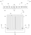
FIGS. 2 a and 2 b illustrate a side cross-sectional view and a top plan view, respectively, of at least one trench formed in a back surface of the microelectronic die of FIG. 1, according to one embodiment of the present description.
FIGS. 3 a-3 d illustrate side cross-sectional views of various embodiments of trench shapes, according to embodiments of the present description.
FIG. 4 illustrates a side cross-sectional view of a seed/barrier layer deposited on the microelectronic die back surface and within the trenches of the structure illustrated in FIG. 2, according to an embodiment of the present description.
FIG. 5 illustrates a side cross-sectional view of a mask patterned on the microelectronic die back surface with at least one opening corresponding to at least one of the trenches of the structure illustrated in FIG. 4, according to an embodiment of the present description.
FIG. 6 illustrates a side cross-sectional view of the trenches of FIG. 5 filled with a thermally conductive material to form at least one heat transfer device, according to an embodiment of the present description.
FIG. 7 illustrates a side cross-sectional view of the structure of FIG. 6 after the removal of the mask, according to an embodiment of the present description.
FIGS. 8 a and 8 b illustrates a side cross-sectional view and a top plan view, respectively, of a microelectronic die having embedded heat dissipation devices located in specific regions of the microelectronic die, according to another embodiment of the present description.
FIGS. 9 a and 9 b illustrates a side cross-sectional view and a top plan view, respectively, of a microelectronic die having an embedded thermoelectric cooling device, according to yet another embodiment of the present description.
FIG. 10 illustrates a side cross-sectional view of a microelectronic die, having an embedded heat dissipation device, attached to a microelectronic structure and having an integrated heat spreading in thermal contract therewith, according to an embodiment of the present description.
FIG. 11 is a flow chart of a process of forming a heat dissipation device within a microelectronic die, according to an embodiment of the present description.
FIG. 12 illustrates an electronic system, according to one embodiment of the present description.
DETAILED DESCRIPTION
In the following detailed description, reference is made to the accompanying drawings that show, by way of illustration, specific embodiments in which the claimed subject matter may be practiced. These embodiments are described in sufficient detail to enable those skilled in the art to practice the subject matter. It is to be understood that the various embodiments, although different, are not necessarily mutually exclusive. For example, a particular feature, structure, or characteristic described herein, in connection with one embodiment, may be implemented within other embodiments without departing from the spirit and scope of the claimed subject matter. In addition, it is to be understood that the location or arrangement of individual elements within each disclosed embodiment may be modified without departing from the spirit and scope of the claimed subject matter. The following detailed description is, therefore, not to be taken in a limiting sense, and the scope of the subject matter is defined only by the appended claims, appropriately interpreted, along with the full range of equivalents to which the appended claims are entitled. In the drawings, like numerals refer to the same or similar elements or functionality throughout the several views, and that elements depicted therein are not necessarily to scale with one another, rather individual elements may be enlarged or reduced in order to more easily comprehend the elements in the context of the present description.
Embodiments of the present description relate to a heat dissipation device that is embedded within a microelectronic die. The heat dissipation device may be fabricated by forming at least one trench extending into the microelectronic die from a microelectronic die back surface, which opposes an active surface thereof, and filling the trenches with at least one layer of thermally conductive material.
As shown in FIG. 1, a microelectronic die 110 may be fabricated or provided, wherein the microelectronic die 110 may include an active surface 112 and an opposing back surface 114. As will be understood to those skilled in the art, the microelectronic die 110 may include an active region 116 proximate the microelectronic die active surface 112, wherein the integrated circuitry (not shown) of the microelectronic die 110 is formed in and/or on the microelectronic die active region 116. The microelectronic die 110 may be formed from any appropriate material, including, but not limited to silicon, germanium, silicon-germanium or III-V compound semiconductor material, and may include a silicon-on-insulator substrate. The microelectronic die 110 may be any appropriate microelectronic device, including, but not limited to a microprocessor, a chipset, a graphics device, a wireless device, a memory device, an application specific integrated circuit device, and the like.
As shown in FIGS. 2 a and 2 b, at least one trench 120 may be formed to extend into the microelectronic die 110 from the microelectronic die back surface 114. The trenches 120 may be formed by any technique known in the art, including, but not limited to, lithography with wet or dry etching, ion bombardment, laser ablation, and the like. Although the trenches 120 of FIGS. 2 a and 2 b are illustrated to run substantially parallel to one another, it is understood that the trenches 120 could form any appropriate pattern. Furthermore, although the trenches 120 are shown in FIG. 2 as having a substantially square shaped in cross-section, it is understood that the trenches 120 may have any appropriate cross-sectional shape including V-shaped (FIG. 3 a), trapezoidal (FIG. 3 b), rectangular (FIG. 3 c), U-shaped (FIG. 3 d), and the like. As will be understood to those skilled in the art, the cross-sectional shape of the trenches 120 may be a function of the technique used to form the trenches 120, as well as the operating parameters used with those techniques.
As shown in FIG. 4, at least one seed and/or a barrier layer 130 may be optionally deposited on the microelectronic die back surface 114 and within the trenches 120. The seed/barrier layer 130 may be formed from any appropriate material and may be deposited by any technique known in the art, including but not limited to, sputtering processes and electro-less plating processes. As will be understood to those skilled in the art, a barrier layer may be utilized to prevent migration of a subsequently deposited material, and a seed layer may be utilized assist in the subsequent plating of a material.
As shown in FIG. 5, a mask 140 may be patterned on the microelectronic die back surface 114 with at least one opening 142 corresponding to at least one of the trenches 120. The mask 140 may be any appropriate material, including but not limited to photoresist materials, such as poly(methyl methacrylate), poly(methyl glutarimide), phenol formaldehyde resin, and the like, and may be patterned by any known technique, including but not limited to, lithographic techniques.
As shown in FIG. 6, the trenches 120 (see FIG. 5) may be filled with an appropriate thermally conductive material 152 to form at least one heat dissipation device 150, and thereby forming a microelectronic device 155 comprising the microelectronic die 110 and the heat dissipation device 150. The filling of the trenches 120 (see FIG. 5) may be achieved by any technique known in the art, including but not limited to electrolytic plating. The thermally conductive material 152 may be any appropriate material including but not limited to metals, such as copper, silver, alloys thereof, and the like. As shown in FIG. 7, the mask 140 (see FIG. 6) may be removed by any appropriate technique known in the art. It is understood that after the removal of the mask 140 (see FIG. 6), the microelectronic die back surface 114 and/or the thermally conductive material 152 may be planarized.
As will be understood to those skilled in the art, the formation of the heat dissipation device 150 may increase the cross-section contact area for heat transfer, thereby enhancing the removal of heat from the microelectronic die 110, without substantially changing a thickness T (see FIG. 2 a), of the microelectronic die 110. It is understood, that trench depth D (see FIG. 2 a), trench spacing S (see FIG. 2 a), and the cross-sectional shape of the trenches 120 (e.g. see FIGS. 2 a and 3 a-3 d) may be varied depending on thermal performance requirements. It is further understood that the trench depth D should not encroach into the active region 116 (e.g. such that no transition performance would be detected). Additionally, it is understood that the thermally conductive material 152 (see FIG. 7) could be selected to have a coefficient of thermal expansion that substantially counteracts warpage during subsequent reflow processes, as will be understood to those skilled in the art.
Although the heat dissipation device 150 is shown to extend substantially across the entire microelectronic die back surface 114 in FIG. 2 b, one of more heat dissipation devices (shown as elements 150 a and 150 b in FIGS. 8 a and 8 b) may be selectively formed over “hot spot regions” (shown as elements 160 a and 160 b in FIGS. 8 a and 8 b). Hot spot regions 160 a and 160 b are areas wherein the greatest amount of heat is generated by the integrated circuitry (not shown) within the microelectronic die 110. The selective formation of the heat dissipation devices 150 a and 150 b may be advantageous in reducing the cost of fabrication depending on the thermal requirements of the microelectronic die 110, as will be understood to those skilled in the art.
In another embodiment of the present description, as shown in FIGS. 9 a and 9 b, the heat dissipation device may be a thermoelectric heat dissipation device (i.e., a Peltier effect device). A thermoelectric heat dissipation device is a solid-state electric heat pump which utilizes electric current to induce a Peltier effect creating a heat flux between an interface between two different conductive materials, thereby transferring heat from one side of the thermoelectric heat dissipation device to the other side thereof. The thermoelectric heat dissipation device (illustrated as element 170) may comprise a first conductive material layer 172 and a second conductive material layer 174 abutting the first conductive material layer 172, both of which are disposed within a trench 120. The first conductive material layer 172 may be electrically connected to a first terminal 182 of a current generating electrical device 180 and the second conductive material layer 174 may be electrically connected to a second terminal 184 of the current generating electrical device 180. The trench 120, the first conductive material layer 172, and the second conductive material layer 174 may be formed by any known techniques including those discussed with regard to FIGS. 1-8 b.
As shown in FIG. 10, the microelectronic die 110 may be attached to a first surface 204 of the microelectronic substrate 202 with a plurality of interconnects 212. The die-to-substrate interconnects 212, such as soldered interconnects, may extend between bond pads 118 formed in or on the microelectronic die active surface 112 of the microelectronic die 110 and substantially mirror-image bond pads 206 in or on the microelectronic substrate first surface 204. An underfill material 224, such as an epoxy material, may be disposed between the microelectronic die active surface 112 and the microelectronic substrate first surface 204.
As further shown in FIG. 10, the microelectronic substrate 202 may provide electrical communication routes (illustrated as dashed lines 208) between the microelectronic die 110 and external components (not shown). As will be understood to those skilled in the art, the microelectronic die bond pads 118 are in electrical communication with integrated circuitry (not shown) within the microelectronic die 110.
As still further illustrated in FIG. 10, an integrated heat spreader 220 may be in thermal contact with the microelectronic die 110, to form a microelectronic system 260. The integrated heat spreader 220 may have a first surface 222 and an opposing second surface 224 in thermal contact with the heat dissipation device 150 embedded in the microelectronic die 110. A thermal interface material 232, such as a thermally conductive grease or polymer, may be disposed between the integrated heat spreader second surface 224 and the heat dissipation device 150 to facilitate heat transfer therebetween. The integrated heat spreader 220 may include at least one footing 242 extending between the integrated heat spreader second surface 224 and the microelectronic substrate 202, wherein the integrated heat spreader footing 242 may be attached to the microelectronic substrate first surface 204 with an adhesive material 252, such as an epoxy material. The integrated heat spreader 220 may be made of any appropriate thermally conductive material, such a metals and alloys, including, but not limited to, copper, aluminum, and the like. It is understood that the integrated heat spreader 220 may be utilized as a load mechanism.
FIG. 11 is a flow chart of a process 300 of fabricating a microelectronic structure according to the various embodiments of the present description. As set forth in block 310, a microelectronic die may be formed having an active surface and an opposing back surface. At least one trench may be formed extending into the microelectronic die from the microelectronic die back surface, as set forth in block 320. As set forth in block 330, the at least one trench may be filled with at least one layer of thermally conductive material.
FIG. 12 illustrates an embodiment of an electronic system/device 400, such as a portable computer, a desktop computer, a mobile telephone, a digital camera, a digital music player, a web tablet/pad device, a personal digital assistant, a pager, an instant messaging device, or other devices. The electronic system/device 400 may be adapted to transmit and/or receive information wirelessly, such as through a wireless local area network (WLAN) system, a wireless personal area network (WPAN) system, and/or a cellular network. The electronic system/device 400 may include a microelectronic motherboard or substrate 410 disposed within a device housing 420. The microelectronic motherboard/substrate 410 may have various electronic components electrically coupled thereto, including a microelectronic device including a microelectronic die and a heat dissipation device disposed therein, as described in the present description (see FIGS. 1-10), and optionally the integrated heat spreader of FIG. 11, all of which are shown generically as element 430. The microelectronic motherboard 410 may be attached to various peripheral devices including an input device 450, such as keypad, and a display device 460, such an LCD display. It is understood that the display device 460 may also function as the input device, if the display device 460 is touch sensitive.
The following examples pertain to further embodiments, wherein Example 1 is a microelectronic device, comprising a microelectronic die having an active surface and an opposing back surface; and at least one heat dissipation device extending into the microelectronic die from the microelectronic die back surface.
In Example 2, the subject matter of Example 1 can optionally include the heat dissipation device comprising at least one layer of thermally conductive material within the at least one trench extending into the microelectronic die.
In Example 3, the subject matter of Example 2 can optionally include the at least one layer of thermally conductive material within the at least one trench comprises a first thermally conductive material layer abutting a second thermally conductive material layer.
In Example 4, the subject matter of Example 3 can optionally include the first thermally conductive material layer in electrical contact with a first terminal of a current generating electrical device and the second thermally conductive material layer in electrical contact with a second terminal of the current generating electronic device.
In Example 5, the subject matter of any of Examples 1 to 4 can optionally include the at least one heat dissipation device positioned proximate a hot spot location in the microelectronic die.
In Example 6, the subject matter of any of Examples 1 to 4 can optionally include the at least one heat dissipation device comprising a thermally conductive material selected from a group consisting of copper and silver.
In Example 7, the subject matter of any of Examples 1 to 4 can optionally include the microelectronic die active surface electrically connected to a microelectronic substrate.
In Example 8, the subject matter of any of Examples 1 to 4 can optionally include an integrated heat spreader in thermal contact with the at least one heat dissipation device.
In Example 9, the subject matter of any of Examples 1 to 4 can optionally include at least one of a seed layer and a barrier layer disposed between the microelectronic die and the at least one heat dissipation device.
The following examples pertain to further embodiments, wherein Example 10 is a method of fabricating a heat dissipation device within a microelectronic die, comprising forming a microelectronic die having an active surface and an opposing back surface; forming at least one trench extending into the microelectronic die from the microelectronic die back surface; and disposing at least one layer of thermally conductive material within the at least one trench.
In Example 11, the subject matter of Example 10 can optionally include the step of disposing at least one layer of thermally conductive material within the at least one trench comprising disposing a first thermally conductive material layer within the at least one trench and disposing a second thermally conductive material layer abutting the first thermally conductive material layer within the at least one trench.
In Example 12, the subject matter of Example 11 can optionally include the electrically contacting the first thermally conductive material layer with a first terminal of a current generating electrical device and electrically contacting the second thermally conductive material layer with a second terminal of the current generating electronic device.
In Example 13, the subject matter of Example 10 can optionally include forming at the least one trench extending into the microelectronic die from the microelectronic die back surface by a technique selected from the group consisting of etching, ion bombardment, and laser ablation.
In Example 14, the subject matter of any of Examples 10 to 13 can optionally include forming at least one of a seed layer and a barrier layer disposed between the at least one trench and the at least one thermally conductive material layer.
In Example 15, the subject matter of any of Examples 10 to 13 can optionally include the step of disposing at least one layer of thermally conductive material within the at least one trench comprising patterning a mask with at least one opening corresponding to the at least one trench; and plating the thermally conductive material within the at least one trench.
In Example 16, the subject matter of Example 15 can optionally include removing the mask.
In Example 17, the subject matter of any of Examples 10 to 13 can optionally include connecting the microelectronic die active surface to a microelectronic substrate.
In Example 18, the subject matter of any of Examples 10 to 13 can optionally include thermally contacting an integrated heat spreader with the heat dissipation device.
In Example 19, the subject matter of any of Examples 10 to 13 can optionally include disposing at least one layer of thermally conductive material selected from a group consisting of copper and silver.
In Example 20, the subject matter of any of Examples 10 to 13 can optionally include forming the at least one heat dissipation device proximate a hot spot location in the microelectronic die.
The following examples pertain to further embodiments, wherein Example 21 is an electronic system, comprising a housing; a microelectronic substrate disposed within the housing; and a microelectronic device comprising: a microelectronic die having an active surface and an opposing back surface electrically attached to the microelectronic surface by the microelectronic die first surface; and a heat dissipation device extending into the microelectronic die from the microelectronic die back surface.
In Example 22, the subject matter of Example 21 can optionally include the heat dissipation device comprising at least one layer of thermally conductive material within the at least one trench extending into the microelectronic die.
In Example 23, the subject matter of Example 22 can optionally include the at least one layer of thermally conductive material within the at least one trench comprising a first thermally conductive material layer abutting a second thermally conductive material layer.
In Example 24, the subject matter Examples 23 can optionally include the first thermally conductive material layer in electrical contact with a first terminal of a current generating electrical device and the second thermally conductive material layer in electrical contact with a second terminal of the current generating electronic device.
In Example 25, the subject matter of any of Examples 21 to 24 can optionally include the at least one heat dissipation device positioned proximate a hot spot location in the microelectronic die.
In Example 26, the subject matter of any of Examples 21 to 24 can optionally include the at least one heat dissipation device comprising a thermally conductive material selected from a group consisting of copper and silver.
In Example 27, the subject matter of any of Examples 21 to 24 can optionally include an integrated heat spreader in thermal contact with the at least one heat dissipation device.
In Example 28, the subject matter of any of Examples 21 to 24 can optionally include at least one of a seed layer and a barrier layer disposed between the microelectronic die and the at least one heat dissipation device.
It is understood that the subject matter of the present description is not necessarily limited to specific applications illustrated in FIGS. 1-12. The subject matter may be applied to other microelectronic device applications, as well as applications outside of the microelectronic industry, as will be understood to those skilled in the art.
Having thus described in detail embodiments of the present invention, it is understood that the invention defined by the appended claims is not to be limited by particular details set forth in the above description, as many apparent variations thereof are possible without departing from the spirit or scope thereof.

Claims (17)

What is claimed is:
1. A microelectronic device, comprising:
a microelectronic die having an active surface and an opposing back surface; and
at least one heat dissipation device extending into, without extending through, the microelectronic die from the microelectronic die back surface, wherein heat dissipation device comprises a first thermally conductive material layer abutting a second thermally conductive material layer and wherein the first thermally conductive material layer is in electrical contact with a first terminal of a current generating electrical device and the second thermally conductive material layer is in electrical contact with a second terminal of the current generating electronic device.
2. The microelectronic device of claim 1, wherein the at least one heat dissipation device is positioned proximate a hot spot location in the microelectronic die.
3. The microelectronic device of claim 1, wherein the microelectronic die active surface is electrically connected to a microelectronic substrate.
4. The microelectronic device of claim 1, further comprising an integrated heat spreader in thermal contact with the at least one heat dissipation device.
5. The microelectronic device of claim 1, further comprising at least one of a seed layer and a barrier layer disposed between the microelectronic die and the at least one heat dissipation device.
6. A method of fabricating a heat dissipation device within a microelectronic die, comprising
forming a microelectronic die having an active surface and an opposing back surface;
forming at least one trench extending into, without extending through, the microelectronic die from the microelectronic die back surface;
disposing a first thermally conductive material within the at least one trench and disposing a second thermally conductive material layer abutting the first thermally conductive material layer within the at least one trench;
electrically contacting the first thermally conductive material layer with a first terminal of a current generating electrical device; and
electrically contacting the second thermally conductive material layer with a second terminal of the current generating electronic device.
7. The method of claim 6, wherein forming at least one trench extending into the microelectronic die from the microelectronic die back surface comprises forming at least one trench extending into the microelectronic die from the microelectronic die back surface by a technique selected from the group consisting of etching, ion bombardment, and laser ablation.
8. The method of claim 6, further comprising forming at least one of a seed layer and a barrier layer disposed between the at least one trench and the at least one thermally conductive material layer.
9. The method of claim 6, wherein disposing at least one layer of thermally conductive material within the at least one trench comprises patterning a mask with at least one opening corresponding to the at least one trench; and plating the thermally conductive material within the at least one trench.
10. The method of claim 9, further including removing the mask.
11. The method of claim 6, further comprising electrically connecting the microelectronic die active surface to a microelectronic substrate.
12. The method of claim 6, further including thermally contacting an integrated heat spreader with the heat dissipation device.
13. The method of claim 6, wherein forming the at least one heat dissipation device comprises forming the at least one heat dissipation device proximate a hot spot location in the microelectronic die.
14. An electronic system, comprising:
a housing;
a microelectronic substrate disposed within the housing; and
a microelectronic device comprising:
a microelectronic die having an active surface and an opposing back surface electrically attached to the microelectronic substrate by the microelectronic die active surface; and
a heat dissipation device extending into, without extending through, the microelectronic die from the microelectronic die back surface, wherein the heat dissipation device comprises a first thermally conductive material layer abutting a second thermally conductive material layer and wherein the first thermally conductive material layer is in electrical contact with a first terminal of a current generating electrical device and the second thermally conductive material layer is in electrical contact with a second terminal of the current generating electronic device.
15. The electronic system of claim 14, wherein the at least one heat dissipation device is positioned proximate a hot spot location in the microelectronic die.
16. The electronic system of claim 14, further comprising an integrated heat spreader in thermal contact with the at least one heat dissipation device.
17. The electronic system of claim 14, further comprising at least one of a seed layer and a barrier layer disposed between the microelectronic die and the at least one heat dissipation device.
US13/904,169 2013-05-29 2013-05-29 Heat dissipation device embedded within a microelectronic die Active US8907461B1 (en)

Priority Applications (1)

Application Number Priority Date Filing Date Title
US13/904,169 US8907461B1 (en) 2013-05-29 2013-05-29 Heat dissipation device embedded within a microelectronic die

Applications Claiming Priority (1)

Application Number Priority Date Filing Date Title
US13/904,169 US8907461B1 (en) 2013-05-29 2013-05-29 Heat dissipation device embedded within a microelectronic die

Publications (2)

Publication Number Publication Date
US20140353817A1 US20140353817A1 (en) 2014-12-04
US8907461B1 true US8907461B1 (en) 2014-12-09

Family

ID=51984217

Family Applications (1)

Application Number Title Priority Date Filing Date
US13/904,169 Active US8907461B1 (en) 2013-05-29 2013-05-29 Heat dissipation device embedded within a microelectronic die

Country Status (1)

Country Link
US (1) US8907461B1 (en)

Families Citing this family (2)

* Cited by examiner, † Cited by third party
Publication number Priority date Publication date Assignee Title
FR3061600B1 (en) * 2017-01-03 2020-06-26 Stmicroelectronics (Grenoble 2) Sas ELECTRONIC DEVICE COMPRISING A GROOVED CHIP
CN111834438A (en) * 2019-04-18 2020-10-27 西部数据技术公司 Aperture structure on backside of semiconductor component for mitigating delamination in stacked package

Citations (9)

* Cited by examiner, † Cited by third party
Publication number Priority date Publication date Assignee Title
US20050257821A1 (en) * 2004-05-19 2005-11-24 Shriram Ramanathan Thermoelectric nano-wire devices
US7029951B2 (en) * 2003-09-12 2006-04-18 International Business Machines Corporation Cooling system for a semiconductor device and method of fabricating same
US7122891B2 (en) * 2003-12-23 2006-10-17 Intel Corporation Ceramic embedded wireless antenna
US7286359B2 (en) * 2004-05-11 2007-10-23 The U.S. Government As Represented By The National Security Agency Use of thermally conductive vias to extract heat from microelectronic chips and method of manufacturing
US20100127388A1 (en) * 2008-11-25 2010-05-27 Stanley Gavin D Metal injection molded heat dissipation device
US7996989B2 (en) * 2003-06-30 2011-08-16 Intel Corporation Heat dissipating device with preselected designed interface for thermal interface materials
US20120092834A1 (en) * 2010-08-12 2012-04-19 Industrial Technology Research Institute Heat dissipation structure for electronic device and fabrication method thereof
US20120161190A1 (en) * 2010-12-22 2012-06-28 Zhimin Jamie Yao Electronic device submounts including substrates with thermally conductive vias
US8275755B2 (en) * 2004-09-15 2012-09-25 International Business Machines Corporation Systems and methods for efficient data searching, storage and reduction

Patent Citations (9)

* Cited by examiner, † Cited by third party
Publication number Priority date Publication date Assignee Title
US7996989B2 (en) * 2003-06-30 2011-08-16 Intel Corporation Heat dissipating device with preselected designed interface for thermal interface materials
US7029951B2 (en) * 2003-09-12 2006-04-18 International Business Machines Corporation Cooling system for a semiconductor device and method of fabricating same
US7122891B2 (en) * 2003-12-23 2006-10-17 Intel Corporation Ceramic embedded wireless antenna
US7286359B2 (en) * 2004-05-11 2007-10-23 The U.S. Government As Represented By The National Security Agency Use of thermally conductive vias to extract heat from microelectronic chips and method of manufacturing
US20050257821A1 (en) * 2004-05-19 2005-11-24 Shriram Ramanathan Thermoelectric nano-wire devices
US8275755B2 (en) * 2004-09-15 2012-09-25 International Business Machines Corporation Systems and methods for efficient data searching, storage and reduction
US20100127388A1 (en) * 2008-11-25 2010-05-27 Stanley Gavin D Metal injection molded heat dissipation device
US20120092834A1 (en) * 2010-08-12 2012-04-19 Industrial Technology Research Institute Heat dissipation structure for electronic device and fabrication method thereof
US20120161190A1 (en) * 2010-12-22 2012-06-28 Zhimin Jamie Yao Electronic device submounts including substrates with thermally conductive vias

Also Published As

Publication number Publication date
US20140353817A1 (en) 2014-12-04

Similar Documents

Publication Publication Date Title
US10616992B2 (en) Circuit board and method for manufacturing the same
KR100865595B1 (en) Thermoelectric nano-wire devices
TWI528504B (en) Wafer level stack die package
KR102240195B1 (en) Integrated thermoelectric cooling
US11756856B2 (en) Package architecture including thermoelectric cooler structures
US20220240370A1 (en) Package substrate inductor having thermal interconnect structures
KR101465616B1 (en) Thermal interface materials(adhesive) and semiconductor chip packages including the same
CN103187372A (en) Chip packaging structure
WO2013172814A1 (en) Microelectronic package utilizing multiple bumpless build-up structures and through-silicon vias
US9099427B2 (en) Thermal energy dissipation using backside thermoelectric devices
US20150179543A1 (en) Three-dimensional integrated circuit structures providing thermoelectric cooling and methods for cooling such integrated circuit structures
CN114730746A (en) Thermally conductive pillar/active die for improved cooling of stacked bottom die
JP2019517128A (en) In-Plane Active Cooling Device for Mobile Electronic Devices
CN102856278A (en) Adapter plate structure and manufacturing method thereof
US8907461B1 (en) Heat dissipation device embedded within a microelectronic die
US11694942B2 (en) Annular silicon-embedded thermoelectric cooling devices for localized on-die thermal management
US20200312741A1 (en) Thermoelectric cooler to enhance thermal-mechanical package performance
US20190206836A1 (en) Stacked semiconductor architecture including semiconductor dies and thermal spreaders on a base die
US10644140B2 (en) Integrated circuit die having back-end-of-line transistors
US20180226322A1 (en) Thermoelectric bonding for integrated circuits
US11664293B2 (en) Solid state thermoelectric cooler in silicon backend layers for fast cooling in turbo scenarios
US11462457B2 (en) Using a thermoelectric cooler to reduce heat transfer between heat-conducting plates
Chau et al. Feasibility study of using solid state refrigeration technologies for electronic cooling
TWI360241B (en) Chip with thermoelectric function
US20210375712A1 (en) Thermal mitigation die using back side etch

Legal Events

Date Code Title Description
FEPP Fee payment procedure

Free format text: PAYOR NUMBER ASSIGNED (ORIGINAL EVENT CODE: ASPN); ENTITY STATUS OF PATENT OWNER: LARGE ENTITY

AS Assignment

Owner name: INTEL CORPORATION, CALIFORNIA

Free format text: ASSIGNMENT OF ASSIGNORS INTEREST;ASSIGNORS:KONCHADY, MANOHAR S.;ROY, MIHIR K.;REEL/FRAME:033014/0920

Effective date: 20130528

STCF Information on status: patent grant

Free format text: PATENTED CASE

MAFP Maintenance fee payment

Free format text: PAYMENT OF MAINTENANCE FEE, 4TH YEAR, LARGE ENTITY (ORIGINAL EVENT CODE: M1551)

Year of fee payment: 4

MAFP Maintenance fee payment

Free format text: PAYMENT OF MAINTENANCE FEE, 8TH YEAR, LARGE ENTITY (ORIGINAL EVENT CODE: M1552); ENTITY STATUS OF PATENT OWNER: LARGE ENTITY

Year of fee payment: 8