US8906715B2 - Light emitting diode package having fluorescent film directly coated on light emitting diode die and method for manufacturing the same - Google Patents

Light emitting diode package having fluorescent film directly coated on light emitting diode die and method for manufacturing the same Download PDF

Info

Publication number
US8906715B2
US8906715B2 US13/600,236 US201213600236A US8906715B2 US 8906715 B2 US8906715 B2 US 8906715B2 US 201213600236 A US201213600236 A US 201213600236A US 8906715 B2 US8906715 B2 US 8906715B2
Authority
US
United States
Prior art keywords
fluorescent film
led die
supporting board
manufacturing
led
Prior art date
Legal status (The legal status is an assumption and is not a legal conclusion. Google has not performed a legal analysis and makes no representation as to the accuracy of the status listed.)
Expired - Fee Related, expires
Application number
US13/600,236
Other versions
US20130161673A1 (en
Inventor
Lung-hsin Chen
Wen-Liang Tseng
Pin-Chuan Chen
Current Assignee (The listed assignees may be inaccurate. Google has not performed a legal analysis and makes no representation or warranty as to the accuracy of the list.)
Advanced Optoelectronic Technology Inc
Original Assignee
Advanced Optoelectronic Technology Inc
Priority date (The priority date is an assumption and is not a legal conclusion. Google has not performed a legal analysis and makes no representation as to the accuracy of the date listed.)
Filing date
Publication date
Application filed by Advanced Optoelectronic Technology Inc filed Critical Advanced Optoelectronic Technology Inc
Assigned to ADVANCED OPTOELECTRONIC TECHNOLOGY, INC. reassignment ADVANCED OPTOELECTRONIC TECHNOLOGY, INC. ASSIGNMENT OF ASSIGNORS INTEREST (SEE DOCUMENT FOR DETAILS). Assignors: CHEN, LUNG-HSIN, CHEN, PIN-CHUAN, TSENG, WEN-LIANG
Publication of US20130161673A1 publication Critical patent/US20130161673A1/en
Application granted granted Critical
Publication of US8906715B2 publication Critical patent/US8906715B2/en
Expired - Fee Related legal-status Critical Current
Adjusted expiration legal-status Critical

Links

Images

Classifications

    • HELECTRICITY
    • H10SEMICONDUCTOR DEVICES; ELECTRIC SOLID-STATE DEVICES NOT OTHERWISE PROVIDED FOR
    • H10HINORGANIC LIGHT-EMITTING SEMICONDUCTOR DEVICES HAVING POTENTIAL BARRIERS
    • H10H20/00Individual inorganic light-emitting semiconductor devices having potential barriers, e.g. light-emitting diodes [LED]
    • H10H20/80Constructional details
    • H10H20/85Packages
    • H10H20/851Wavelength conversion means
    • H10H20/8514Wavelength conversion means characterised by their shape, e.g. plate or foil
    • HELECTRICITY
    • H01ELECTRIC ELEMENTS
    • H01LSEMICONDUCTOR DEVICES NOT COVERED BY CLASS H10
    • H01L2224/00Indexing scheme for arrangements for connecting or disconnecting semiconductor or solid-state bodies and methods related thereto as covered by H01L24/00
    • H01L2224/01Means for bonding being attached to, or being formed on, the surface to be connected, e.g. chip-to-package, die-attach, "first-level" interconnects; Manufacturing methods related thereto
    • H01L2224/42Wire connectors; Manufacturing methods related thereto
    • H01L2224/47Structure, shape, material or disposition of the wire connectors after the connecting process
    • H01L2224/48Structure, shape, material or disposition of the wire connectors after the connecting process of an individual wire connector
    • H01L2224/4805Shape
    • H01L2224/4809Loop shape
    • H01L2224/48091Arched
    • HELECTRICITY
    • H10SEMICONDUCTOR DEVICES; ELECTRIC SOLID-STATE DEVICES NOT OTHERWISE PROVIDED FOR
    • H10HINORGANIC LIGHT-EMITTING SEMICONDUCTOR DEVICES HAVING POTENTIAL BARRIERS
    • H10H20/00Individual inorganic light-emitting semiconductor devices having potential barriers, e.g. light-emitting diodes [LED]
    • H10H20/01Manufacture or treatment
    • H10H20/036Manufacture or treatment of packages
    • H10H20/0361Manufacture or treatment of packages of wavelength conversion means
    • HELECTRICITY
    • H10SEMICONDUCTOR DEVICES; ELECTRIC SOLID-STATE DEVICES NOT OTHERWISE PROVIDED FOR
    • H10HINORGANIC LIGHT-EMITTING SEMICONDUCTOR DEVICES HAVING POTENTIAL BARRIERS
    • H10H20/00Individual inorganic light-emitting semiconductor devices having potential barriers, e.g. light-emitting diodes [LED]
    • H10H20/80Constructional details
    • H10H20/85Packages
    • H10H20/8506Containers

Definitions

  • the present disclosure generally relates to a light emitting diode (LED) package and method for manufacturing the same, and particularly to an LED package wherein a fluorescent film directly and conformably covers an LED die and a method for manufacturing the same.
  • LED light emitting diode
  • LEDs light emitting diodes
  • a common LED includes a substrate, electrodes arranged on the substrate, a reflective cup arranged on the substrate, an LED die arranged in the reflective cup and electrically connected to the electrodes, an encapsulation covering the LED die, and a fluorescent film coated on an outer surface of the encapsulation.
  • the fluorescent substance In packaging process of common LEDs, the fluorescent substance is firstly mixed in fluid encapsulating material, then the fluid encapsulating material is sprayed on the outer surface of the encapsulation, and finally the encapsulating material mixed with fluorescent substance is solidified.
  • the fluid encapsulating material cannot be completely uniformly sprayed on the encapsulation, due to an operational tolerance of the spray tool. Therefore the fluorescent film will be non-uniform in thickness.
  • the fluorescent substance suspending in the encapsulating material will deposit and undesirably cause a non-uniform distribution of the fluorescent substance in the encapsulating material.
  • the uneven distribution of the fluorescent substance in the encapsulating material and the uneven fluorescent film cause light generated by the common LED to have an uneven color.
  • FIG. 1 is a schematic, cross-sectional view of an LED package in accordance with a first embodiment of the present disclosure.
  • FIG. 2 is a schematic, cross-sectional view of an LED package in accordance with a second embodiment of the present disclosure.
  • FIG. 3 is a flow chart of a method for forming the LED package in accordance with the first embodiment of the present disclosure.
  • FIGS. 4-8 are schematic cross sections showing an LED package in accordance with the first embodiment of the present disclosure processed by various steps of the LED packaging method of FIG. 3 .
  • an LED package 100 of a first embodiment is provided.
  • the LED package 100 includes a substrate 11 , a circuit structure 12 , an LED die 13 , a fluorescent film 14 , a reflective cup 15 , and an encapsulation 16 .
  • the circuit structure 12 is formed on the substrate 11 .
  • the LED die 13 is mounted on the substrate 11 and electrically connected to the circuit structure 12 .
  • the fluorescent film 14 is attached on a top surface of the LED die 13 .
  • the reflective cup 15 is formed on the substrate 11 and surrounds the LED die 13 .
  • the encapsulation 16 covers the LED die 13 on the substrate 11 and the fluorescent film 14 on the LED die 13 .
  • the LED die 13 is arranged on the circuit structure 12 and electrically connected to the circuit structure 12 by wire bonding. More specifically, the circuit structure 12 includes two circuit pads. The LED die 13 is secured to one of the circuit pads by heat conductive and electrically insulating glue and electrically connected to the two circuit pads by wire bonding.
  • the LED die 13 includes a light outputting surface 131 on a top of the LED die 13 and facing away from the substrate 11 . Two electrode pads 132 are formed on the light outputting surface 131 and protrude upwards from the light outputting surface 131 . The electrode pads 132 on the top surface of the LED die 13 are connected to the circuit structure 12 by two metal wires 133 .
  • the fluorescent film 14 is attached on the light outputting surface 131 of the LED die 13 .
  • the fluorescent film 14 includes two through holes 141 .
  • a size of each through hole 141 is similar to that of each electrode pad 132 of the LED die 13 , and a position of each through hole 141 is corresponding to each electrode pad 132 of the LED die 13 , whereby the electrode pads 132 can be fittingly received in through holes 141 .
  • the electrode pads 132 respectively penetrate through the two through-holes 141 , and are exposed out of the fluorescent film 14 .
  • an LED package 200 according to a second embodiment is provided.
  • the LED package 200 includes a substrate 11 , a circuit structure 12 formed on the substrate 11 , an LED die 23 mounted on the substrate 11 and electrically connected to the circuit structure 12 , a fluorescent film 24 attached on a surface of the LED die 23 , a reflective cup 15 formed on the substrate 11 and surrounding the LED die 23 , and an encapsulation 16 covering the LED die 23 on the substrate 11 .
  • a bonding of the LED die 23 to the circuit structure 12 and a form of the fluorescent film 24 of the LED package 200 in the second embodiment are different from the LED package 100 of the first embodiment.
  • the LED die 23 are bonded on the circuit structure 12 by flip chip bonding.
  • the LED die 23 includes a light outputting surface 231 and two electrode pads 232 formed on a surface of the LED die 23 away from the light outputting surface 231 .
  • the two electrode pads 232 are directly electrically connected to the circuit pads of the circuit structure 12 , respectively.
  • the fluorescent film 24 covers the light outputting surface 231 of the LED die 23 totally, without any through holes formed therein.
  • a method for manufacturing the LED package 100 in accordance with the first embodiment of the present disclosure includes steps of:
  • a supporting board 30 with a flat upper surface 31 is provided.
  • a gel 40 evenly mixed with fluorescent powders therein is dripped on the upper surface 31 of the supporting board 30 .
  • a scraper 50 is positioned above the upper surface 31 with a distance therebetween.
  • the scraper 50 can move over the supporting board 30 along a direction parallel to the upper surface 31 thereof.
  • the scraper 50 is capable of scraping the gel 40 over the upper surface 31 , along a direction parallel to the upper surface 31 of the supporting board 30 .
  • the distance D between a bottom edge of the scraper 50 and the upper surface 31 of the supporting board 30 is smaller than a height H of the gel 40 applied on the upper surface 31 of the supporting board 30 .
  • step 2 referring to FIG. 5 , the gel 40 is scraped over the supporting board 30 by the scraper 50 to form the gelatinous fluorescent film 41 , and then the gelatinous fluorescent film 41 is then solidified to form the fluorescent film 14 .
  • a thickness of the gelatinous fluorescent film 41 is equal to the distance D between the bottom edge of the scraper 50 and the upper surface 31 of the supporting board 30 .
  • the scrapping of the gel 40 to form the gelatinous fluorescent film 41 can be achieved by a relative movement between the scraper 50 and the supporting board 30 .
  • the supporting board 30 is a movable relative to the scraper 50 while the scraper 50 is fixed in position.
  • the scraper 50 is moveable over the supporting board 30 which is fixed in position.
  • the scraper 50 is positioned above the supporting board 30 with the distance D therebetween.
  • the thickness of the gelatinous fluorescent film 41 can be changed according to actual requirement, by adjusting the distance between the scraper 50 and the supporting board 30 .
  • the gelatinous fluorescent film 41 is formed by the scraping process. Then the gelatinous fluorescent film 41 is solidified to form the solidified fluorescent film 14 .
  • the fluorescent substance suspending in the gel 40 will not deposit before the gel 40 is solidified, thereby avoiding a non-uniform distribution of the fluorescent substance in the fluorescent film 14 . Accordingly, it can be avoided that the uneven distribution of fluorescent particles in the fluorescent film 14 to cause light generated by the common LED to have an uneven color.
  • the concentration of the fluorescent substance in the fluorescent film 14 can be adjusted easily to meet different requirements.
  • the thickness of the fluorescent film 14 can be easily controlled to be uniform through its entire length, whereby the uniformity of color of light generated by the LED package 100 can be further guaranteed.
  • step 3 referring to FIG. 6 , the solidified fluorescent film 14 is cut into several individual pieces each with two through holes 141 defined therein, and peeled from the supporting board 30 . Further, a size of each piece of the solidified fluorescent film 14 is substantially equal to that of the light outputting surface 131 of the LED die 13 , whereby the piece of the fluorescent film 14 can cover the light outputting surface 131 of the LED die 13 totally.
  • the position of each through hole 141 is corresponding to one of the electrode pads 132 of the LED die 13 , whereby electrode pads 132 can fittingly extend in the through holes 141 , respectively.
  • the through holes 141 can be formed by cutting, punching or etching.
  • a polyester film can be employed during the peeling of the solidified fluorescent film 14 from the supporting board 30 , by the following steps: attaching a polyester film on a surface of the solidified fluorescent film 14 away from the supporting board 30 to make the fluorescent film 14 adhered to the polyester film, and then rolling up the polyester film together with the solid fluorescent film 14 .
  • the solidified fluorescent film 14 is rolled up together with the polyester film for easy storage.
  • step 4 referring to FIG. 7 , the fluorescent film 14 is attached on a light outputting surface 131 of an LED die 13 . Electrode pads 132 of the LED die 13 respectively penetrate through the two through holes 141 of the solidified fluorescent film 14 and are exposed out of the solidified fluorescent film 14 .
  • step 5 referring to FIG. 8 , the LED die 13 is mounted on a substrate 11 and electrically connected to a circuit structure 12 by wire bonding with metal wires 133 electrically connecting the electrode pads 132 and the circuit structure 12 .
  • a reflective cup 15 is also formed on the substrate 11 , surrounding the LED die 13 .
  • an encapsulation 16 is formed on the substrate 11 and covers the LED die 13 , the wires 133 and the fluorescent film 14 to obtain an LED package. Furthermore, in this embodiment, the encapsulation 16 is filled in the reflective cup 15 to obtain an LED package 100 as shown in FIG. 1 .
  • the step 4 can be exchanged with the step 5 . That is, the fluorescent film 14 can be attached on the light outputting surface 131 of the LED die 13 after the LED die 13 is mounted on the substrate 11 .
  • the method for manufacturing the LED package 200 in accordance with the second embodiment of the present disclosure is similar to the method for manufacturing the LED package 100 of the first embodiment. What is different is that, in this embodiment, the fluorescent film 14 can be directly cut into several individual pieces without any through hole defined therein. Then, each piece of the fluorescent films 14 is attached on a light outputting surface 231 of an LED die 23 . The LED die 23 is mounted on the substrate 11 and connected to the circuit structure 12 by flip chip bonding.
  • the gelatinous fluorescent film 41 is made as a thin film by scraping the gel 40 doped with fluorescent substance firstly, and then solidified to form the solid fluorescent film 14 .
  • the fluorescent substance suspending in the gelatinous fluorescent film 41 can be uniformly distributed in the thin gelatinous fluorescent film 41 without causing a serious deposition. Accordingly, an even concentration of the fluorescent substance suspending in the gelatinous encapsulating glue 40 can be achieved and the thickness of the solidified fluorescent film 14 can be easily controlled, whereby a requirement of the solidified fluorescent film 14 to obtain a light with a uniform color can be assured.

Landscapes

  • Led Device Packages (AREA)

Abstract

A method for packaging an LED, includes steps: providing a supporting board and then dripping a gel mixed with fluorescent therein on the supporting board; scraping the gel over the supporting board with a scraper form a gelatinous fluorescent film on the supporting board, and solidifying the gelatinous fluorescent film pieces to form a solidified fluorescent film; cutting the solidified fluorescent film into individual pieces, and peeling the solid fluorescent films from the supporting board; attaching one piece of the fluorescent film on a light outputting surface of an LED die; mounting the LED die on a substrate, and electrically connecting the LED die to the circuit structure; and forming an encapsulation on the substrate to cover the LED die.

Description

BACKGROUND
1. Technical Field
The present disclosure generally relates to a light emitting diode (LED) package and method for manufacturing the same, and particularly to an LED package wherein a fluorescent film directly and conformably covers an LED die and a method for manufacturing the same.
2. Description of Related Art
In recent years, due to excellent light quality and high luminous efficiency, light emitting diodes (LEDs) have increasingly been used as substitutes for incandescent bulbs, compact fluorescent lamps and fluorescent tubes as light sources of illumination devices.
A common LED includes a substrate, electrodes arranged on the substrate, a reflective cup arranged on the substrate, an LED die arranged in the reflective cup and electrically connected to the electrodes, an encapsulation covering the LED die, and a fluorescent film coated on an outer surface of the encapsulation.
In packaging process of common LEDs, the fluorescent substance is firstly mixed in fluid encapsulating material, then the fluid encapsulating material is sprayed on the outer surface of the encapsulation, and finally the encapsulating material mixed with fluorescent substance is solidified. However, during the spraying process, the fluid encapsulating material cannot be completely uniformly sprayed on the encapsulation, due to an operational tolerance of the spray tool. Therefore the fluorescent film will be non-uniform in thickness. Further, the fluorescent substance suspending in the encapsulating material will deposit and undesirably cause a non-uniform distribution of the fluorescent substance in the encapsulating material. The uneven distribution of the fluorescent substance in the encapsulating material and the uneven fluorescent film cause light generated by the common LED to have an uneven color.
Therefore, what is needed is to provide an LED package and method of manufacturing the same which can overcome the above shortcomings.
BRIEF DESCRIPTION OF THE DRAWINGS
Many aspects of the disclosure can be better understood with reference to the following drawings. The components in the drawings are not necessarily drawn to scale, the emphasis instead being placed upon clearly illustrating the principles of the disclosure.
FIG. 1 is a schematic, cross-sectional view of an LED package in accordance with a first embodiment of the present disclosure.
FIG. 2 is a schematic, cross-sectional view of an LED package in accordance with a second embodiment of the present disclosure.
FIG. 3 is a flow chart of a method for forming the LED package in accordance with the first embodiment of the present disclosure.
FIGS. 4-8 are schematic cross sections showing an LED package in accordance with the first embodiment of the present disclosure processed by various steps of the LED packaging method of FIG. 3.
DETAILED DESCRIPTION
Reference will now be made to the drawings to describe the present LED packages, and a method for making the LED packages, in detail.
Referring to FIG. 1, an LED package 100 of a first embodiment is provided. The LED package 100 includes a substrate 11, a circuit structure 12, an LED die 13, a fluorescent film 14, a reflective cup 15, and an encapsulation 16. The circuit structure 12 is formed on the substrate 11. The LED die 13 is mounted on the substrate 11 and electrically connected to the circuit structure 12. The fluorescent film 14 is attached on a top surface of the LED die 13. The reflective cup 15 is formed on the substrate 11 and surrounds the LED die 13. The encapsulation 16 covers the LED die 13 on the substrate 11 and the fluorescent film 14 on the LED die 13.
The LED die 13 is arranged on the circuit structure 12 and electrically connected to the circuit structure 12 by wire bonding. More specifically, the circuit structure 12 includes two circuit pads. The LED die 13 is secured to one of the circuit pads by heat conductive and electrically insulating glue and electrically connected to the two circuit pads by wire bonding. The LED die 13 includes a light outputting surface 131 on a top of the LED die 13 and facing away from the substrate 11. Two electrode pads 132 are formed on the light outputting surface 131 and protrude upwards from the light outputting surface 131. The electrode pads 132 on the top surface of the LED die 13 are connected to the circuit structure 12 by two metal wires 133.
The fluorescent film 14 is attached on the light outputting surface 131 of the LED die 13. The fluorescent film 14 includes two through holes 141. A size of each through hole 141 is similar to that of each electrode pad 132 of the LED die 13, and a position of each through hole 141 is corresponding to each electrode pad 132 of the LED die 13, whereby the electrode pads 132 can be fittingly received in through holes 141. The electrode pads 132 respectively penetrate through the two through-holes 141, and are exposed out of the fluorescent film 14.
Referring to FIG. 2, an LED package 200 according to a second embodiment is provided. The LED package 200 includes a substrate 11, a circuit structure 12 formed on the substrate 11, an LED die 23 mounted on the substrate 11 and electrically connected to the circuit structure 12, a fluorescent film 24 attached on a surface of the LED die 23, a reflective cup 15 formed on the substrate 11 and surrounding the LED die 23, and an encapsulation 16 covering the LED die 23 on the substrate 11. A bonding of the LED die 23 to the circuit structure 12 and a form of the fluorescent film 24 of the LED package 200 in the second embodiment are different from the LED package 100 of the first embodiment. In this embodiment, the LED die 23 are bonded on the circuit structure 12 by flip chip bonding. The LED die 23 includes a light outputting surface 231 and two electrode pads 232 formed on a surface of the LED die 23 away from the light outputting surface 231. The two electrode pads 232 are directly electrically connected to the circuit pads of the circuit structure 12, respectively. The fluorescent film 24 covers the light outputting surface 231 of the LED die 23 totally, without any through holes formed therein.
A method for manufacturing the LED package 100 in accordance with the first embodiment of the present disclosure includes steps of:
    • Step 1: providing a supporting board and then dripping a gel mixed with fluorescent therein on the supporting board;
    • Step 2: scraping the gel over the supporting board with a scraper form a gelatinous fluorescent film on the supporting board, and solidifying the gelatinous fluorescent film to form a solidified fluorescent film;
    • Step 3: cutting the solidified fluorescent film into individual pieces each with two through holes defined therein, and peeling the solidified fluorescent film pieces from the supporting board;
    • Step 4: attaching one piece of the fluorescent film on a light outputting surface of an LED die with electrode pads of the LED die penetrating through the two through holes;
    • Step 5: mounting the LED die on one of two circuit pads of a circuit structure on a substrate, and electrically connecting the electrode pads of the LED die to the circuit pads of the circuit structure by wire bonding;
    • Step 6: forming an encapsulation on the substrate to cover the LED die, the wires and the piece of the solidified fluorescent film.
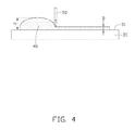
In step 1, referring to FIG. 4, a supporting board 30 with a flat upper surface 31 is provided. A gel 40 evenly mixed with fluorescent powders therein is dripped on the upper surface 31 of the supporting board 30. A scraper 50 is positioned above the upper surface 31 with a distance therebetween. The scraper 50 can move over the supporting board 30 along a direction parallel to the upper surface 31 thereof. In other words, the scraper 50 is capable of scraping the gel 40 over the upper surface 31, along a direction parallel to the upper surface 31 of the supporting board 30. The distance D between a bottom edge of the scraper 50 and the upper surface 31 of the supporting board 30 is smaller than a height H of the gel 40 applied on the upper surface 31 of the supporting board 30.
In step 2, referring to FIG. 5, the gel 40 is scraped over the supporting board 30 by the scraper 50 to form the gelatinous fluorescent film 41, and then the gelatinous fluorescent film 41 is then solidified to form the fluorescent film 14.
A thickness of the gelatinous fluorescent film 41 is equal to the distance D between the bottom edge of the scraper 50 and the upper surface 31 of the supporting board 30. The scrapping of the gel 40 to form the gelatinous fluorescent film 41 can be achieved by a relative movement between the scraper 50 and the supporting board 30. In this embodiment, the supporting board 30 is a movable relative to the scraper 50 while the scraper 50 is fixed in position. Alternatively, the scraper 50 is moveable over the supporting board 30 which is fixed in position. The scraper 50 is positioned above the supporting board 30 with the distance D therebetween. The thickness of the gelatinous fluorescent film 41 can be changed according to actual requirement, by adjusting the distance between the scraper 50 and the supporting board 30.
Accordingly, the gelatinous fluorescent film 41 is formed by the scraping process. Then the gelatinous fluorescent film 41 is solidified to form the solidified fluorescent film 14. The fluorescent substance suspending in the gel 40 will not deposit before the gel 40 is solidified, thereby avoiding a non-uniform distribution of the fluorescent substance in the fluorescent film 14. Accordingly, it can be avoided that the uneven distribution of fluorescent particles in the fluorescent film 14 to cause light generated by the common LED to have an uneven color. Furthermore, the concentration of the fluorescent substance in the fluorescent film 14 can be adjusted easily to meet different requirements. Finally, the thickness of the fluorescent film 14 can be easily controlled to be uniform through its entire length, whereby the uniformity of color of light generated by the LED package 100 can be further guaranteed.
In step 3, referring to FIG. 6, the solidified fluorescent film 14 is cut into several individual pieces each with two through holes 141 defined therein, and peeled from the supporting board 30. Further, a size of each piece of the solidified fluorescent film 14 is substantially equal to that of the light outputting surface 131 of the LED die 13, whereby the piece of the fluorescent film 14 can cover the light outputting surface 131 of the LED die 13 totally. The position of each through hole 141 is corresponding to one of the electrode pads 132 of the LED die 13, whereby electrode pads 132 can fittingly extend in the through holes 141, respectively. The through holes 141 can be formed by cutting, punching or etching.
A polyester film can be employed during the peeling of the solidified fluorescent film 14 from the supporting board 30, by the following steps: attaching a polyester film on a surface of the solidified fluorescent film 14 away from the supporting board 30 to make the fluorescent film 14 adhered to the polyester film, and then rolling up the polyester film together with the solid fluorescent film 14. As such, the solidified fluorescent film 14 is rolled up together with the polyester film for easy storage. When use the polyester film and the fluorescent film 14 are unfolded and subject to a radiation to release the sticking nature of the polyester film, whereby the fluorescent film 14 can be easily removed from the polyester film to be applied to the light outputting surface 131 of the LED die 13.
In step 4, referring to FIG. 7, the fluorescent film 14 is attached on a light outputting surface 131 of an LED die 13. Electrode pads 132 of the LED die 13 respectively penetrate through the two through holes 141 of the solidified fluorescent film 14 and are exposed out of the solidified fluorescent film 14.
In step 5, referring to FIG. 8, the LED die 13 is mounted on a substrate 11 and electrically connected to a circuit structure 12 by wire bonding with metal wires 133 electrically connecting the electrode pads 132 and the circuit structure 12. In this embodiment, a reflective cup 15 is also formed on the substrate 11, surrounding the LED die 13.
In step 6, an encapsulation 16 is formed on the substrate 11 and covers the LED die 13, the wires 133 and the fluorescent film 14 to obtain an LED package. Furthermore, in this embodiment, the encapsulation 16 is filled in the reflective cup 15 to obtain an LED package 100 as shown in FIG. 1.
The step 4 can be exchanged with the step 5. That is, the fluorescent film 14 can be attached on the light outputting surface 131 of the LED die 13 after the LED die 13 is mounted on the substrate 11.
The method for manufacturing the LED package 200 in accordance with the second embodiment of the present disclosure is similar to the method for manufacturing the LED package 100 of the first embodiment. What is different is that, in this embodiment, the fluorescent film 14 can be directly cut into several individual pieces without any through hole defined therein. Then, each piece of the fluorescent films 14 is attached on a light outputting surface 231 of an LED die 23. The LED die 23 is mounted on the substrate 11 and connected to the circuit structure 12 by flip chip bonding.
In this process, the gelatinous fluorescent film 41 is made as a thin film by scraping the gel 40 doped with fluorescent substance firstly, and then solidified to form the solid fluorescent film 14. The fluorescent substance suspending in the gelatinous fluorescent film 41 can be uniformly distributed in the thin gelatinous fluorescent film 41 without causing a serious deposition. Accordingly, an even concentration of the fluorescent substance suspending in the gelatinous encapsulating glue 40 can be achieved and the thickness of the solidified fluorescent film 14 can be easily controlled, whereby a requirement of the solidified fluorescent film 14 to obtain a light with a uniform color can be assured.
It is to be understood that the above-described embodiments are intended to illustrate rather than limit the disclosure. Variations may be made to the embodiments without departing from the spirit of the disclosure as claimed. The above-described embodiments illustrate the scope of the disclosure but do not restrict the scope of the disclosure.

Claims (10)

What is claimed is:
1. A method for manufacturing an LED package, comprising steps:
providing a supporting board and then dripping a gel mixed with fluorescent therein on the supporting board;
scraping the gel over the supporting board with a scraper form a gelatinous fluorescent film on the supporting board, and solidifying the gelatinous fluorescent film pieces to form a solidified fluorescent film;
cutting the solidified fluorescent film into individual pieces, and peeling the solid fluorescent films from the supporting board;
defining two through-holes in the solidified fluorescent film;
attaching one piece of the fluorescent film on a light outputting surface of an LED die;
mounting the LED die on a substrate, and electrically connecting the LED die to the circuit structure; and
forming an encapsulation on the substrate to cover the LED die.
2. The method for manufacturing the LED package of claim 1, wherein the supporting board comprises a flat upper surface, a distance between a bottom edge of the scraper and the upper surface of the supporting board being smaller than a proposed thickness of the gel.
3. The method for manufacturing the LED package of claim 2, wherein the substrate is a movable relative to the scraper while the scraper is fixed in position.
4. The method for manufacturing the LED package of claim 1, wherein the LED die comprises two electrode pads, and the two electrode pads are formed on a surface of the LED die away from the light outputting surface of an LED die.
5. The method for manufacturing the LED package of claim 4, wherein the LED die is mounted on the substrate and electrically connected to the circuit board by flip chip bonding.
6. The method for manufacturing the LED package of claim 1, wherein the LED die comprises two electrode pads, and the two electrode pads are positioned on the light outputting surface of an LED die.
7. The method for manufacturing the LED package of claim 1, wherein the solidified fluorescent film is attached on the light outputting surface of the LED die with the electrode pads penetrating through the two through-holes.
8. The method for manufacturing the LED package of claim 1, wherein the through-holes are made by cutting, etching or punching.
9. The method for manufacturing the LED package of claim 6, wherein the LED die is mounted on the substrate and connected to the circuit board by wire bonding.
10. A method for manufacturing a solid fluorescent film, comprising steps:
providing a supporting board and then dripping a gel mixed with fluorescent therein on the supporting board;
scraping the gel over the supporting board with a scraper form a gelatinous fluorescent film on the supporting board, and solidifying the gelatinous fluorescent film pieces to form a solidified fluorescent film;
cutting the solidified fluorescent film into individual pieces, and peeling the solid fluorescent films from the supporting board;
defining two through-holes in the solidified fluorescent film.
US13/600,236 2011-12-27 2012-08-31 Light emitting diode package having fluorescent film directly coated on light emitting diode die and method for manufacturing the same Expired - Fee Related US8906715B2 (en)

Applications Claiming Priority (3)

Application Number Priority Date Filing Date Title
CN2011104441743A CN103187486A (en) 2011-12-27 2011-12-27 Manufacturing methods of package structure of light emitting diode and fluorescent thin films of package structure
CN201110444174 2011-12-27
CN201110444174.3 2011-12-27

Publications (2)

Publication Number Publication Date
US20130161673A1 US20130161673A1 (en) 2013-06-27
US8906715B2 true US8906715B2 (en) 2014-12-09

Family

ID=48653661

Family Applications (1)

Application Number Title Priority Date Filing Date
US13/600,236 Expired - Fee Related US8906715B2 (en) 2011-12-27 2012-08-31 Light emitting diode package having fluorescent film directly coated on light emitting diode die and method for manufacturing the same

Country Status (4)

Country Link
US (1) US8906715B2 (en)
JP (1) JP2013138206A (en)
CN (1) CN103187486A (en)
TW (1) TWI478398B (en)

Families Citing this family (6)

* Cited by examiner, † Cited by third party
Publication number Priority date Publication date Assignee Title
CN104576890A (en) * 2013-10-17 2015-04-29 刘艳 Method for forming fluorescent layer on LED chip
CN104576889B (en) * 2013-10-17 2018-10-26 刘艳 The method that fluorescence coating is formed in LED chip
CN105047800A (en) * 2014-09-19 2015-11-11 秦水林 Method for manufacturing LED phosphorous films
CN108352434A (en) * 2015-11-10 2018-07-31 亿光电子工业股份有限公司 Light emitting diode device and manufacturing method thereof
CN108281534A (en) * 2018-01-05 2018-07-13 福建天电光电有限公司 A kind of emitting semiconductor structure and its preparation process that can send out a variety of coloured light
CN111660592A (en) * 2020-06-09 2020-09-15 福建天电光电有限公司 Process for manufacturing solid fluorescent membrane based on glue scraping equipment

Citations (8)

* Cited by examiner, † Cited by third party
Publication number Priority date Publication date Assignee Title
JP2003101074A (en) 2001-09-26 2003-04-04 Stanley Electric Co Ltd Light emitting device
US20080121911A1 (en) 2006-11-28 2008-05-29 Cree, Inc. Optical preforms for solid state light emitting dice, and methods and systems for fabricating and assembling same
WO2008126500A1 (en) 2007-03-28 2008-10-23 Hiroshima University M-c-n-o fluorescent substance
US20080290351A1 (en) 2007-05-24 2008-11-27 Shuichi Ajiki Semiconductor light emitting apparatus
CN101486854A (en) * 2008-01-15 2009-07-22 财团法人工业技术研究院 Ink composition of photochromic conversion film and preparation method thereof
US20110163300A1 (en) * 2010-01-06 2011-07-07 National Chiao Tung University Organic light-emitting material, organic light-emitting element using the same and method of forming the same
WO2012081411A1 (en) 2010-12-13 2012-06-21 東レ株式会社 Phosphor sheet, led and light emitting device using same and method for producing led
WO2012144030A1 (en) 2011-04-20 2012-10-26 株式会社エルム Light emitting device and method for manufacturing same

Family Cites Families (1)

* Cited by examiner, † Cited by third party
Publication number Priority date Publication date Assignee Title
JP2011222852A (en) * 2010-04-13 2011-11-04 Nitto Denko Corp Optical semiconductor device

Patent Citations (14)

* Cited by examiner, † Cited by third party
Publication number Priority date Publication date Assignee Title
JP2003101074A (en) 2001-09-26 2003-04-04 Stanley Electric Co Ltd Light emitting device
US20080121911A1 (en) 2006-11-28 2008-05-29 Cree, Inc. Optical preforms for solid state light emitting dice, and methods and systems for fabricating and assembling same
JP2008166740A (en) 2006-11-28 2008-07-17 Cree Inc Optical preform for solid state light emitting die and method and system for its fabrication and assembly
WO2008126500A1 (en) 2007-03-28 2008-10-23 Hiroshima University M-c-n-o fluorescent substance
US20100109508A1 (en) 2007-03-28 2010-05-06 Hiroshima University M-c-n-o based phosphor
US20140077237A1 (en) 2007-05-24 2014-03-20 Stanley Electric Co., Ltd. Semiconductor light emitting apparatus
US20080290351A1 (en) 2007-05-24 2008-11-27 Shuichi Ajiki Semiconductor light emitting apparatus
JP2008294224A (en) 2007-05-24 2008-12-04 Stanley Electric Co Ltd Semiconductor light emitting device
CN101486854A (en) * 2008-01-15 2009-07-22 财团法人工业技术研究院 Ink composition of photochromic conversion film and preparation method thereof
TW201124362A (en) 2010-01-06 2011-07-16 Univ Nat Chiao Tung Organic light emitting matterial
US20110163300A1 (en) * 2010-01-06 2011-07-07 National Chiao Tung University Organic light-emitting material, organic light-emitting element using the same and method of forming the same
WO2012081411A1 (en) 2010-12-13 2012-06-21 東レ株式会社 Phosphor sheet, led and light emitting device using same and method for producing led
US20130264601A1 (en) 2010-12-13 2013-10-10 Toray Industries, Inc. Phosphor sheet, led and light emitting device using the same and method for manufacturing led (as amended)
WO2012144030A1 (en) 2011-04-20 2012-10-26 株式会社エルム Light emitting device and method for manufacturing same

Also Published As

Publication number Publication date
TWI478398B (en) 2015-03-21
CN103187486A (en) 2013-07-03
US20130161673A1 (en) 2013-06-27
TW201327934A (en) 2013-07-01
JP2013138206A (en) 2013-07-11

Similar Documents

Publication Publication Date Title
US8906715B2 (en) Light emitting diode package having fluorescent film directly coated on light emitting diode die and method for manufacturing the same
TWI630731B (en) White light emitting diode component
US9735198B2 (en) Substrate based light emitter devices, components, and related methods
US9512968B2 (en) LED module
US9012248B2 (en) Method for packaging light emitting diode
US10847691B2 (en) LED flip chip structures with extended contact pads formed by sintering silver
US20130161670A1 (en) Light emitting diode packages and methods of making
JP5860289B2 (en) Manufacturing method of LED device
JP2015502021A (en) Flexible light-emitting semiconductor device having a three-dimensional structure
CN104393154A (en) Wafer level packaging method for LED (Light-Emitting Diode) chip level white light source
CN102779923A (en) Manufacturing method of patch type LED (Light-Emitting Diode) module
US20130037830A1 (en) Light emitting diode package and method for manufacturing the same
CN104134741A (en) Packaging method for LED (Light-Emitting Diode) display screen module
US7811843B1 (en) Method of manufacturing light-emitting diode
TW201322501A (en) Light-emitting diode mixing chamber having a reflective wall formed in the trench
TWI455371B (en) Method for manufacturing light emitting diode package structure
US10797204B2 (en) Submount based light emitter components and methods
US20160172554A1 (en) Pc led with optical element and without ssubstrate carrier
CN105280781A (en) A flip-chip white light LED device and manufacturing method thereof
JP2013168647A (en) Method of manufacturing fluorescent film and method of manufacturing light-emitting diode package
TW201351709A (en) Light emitting diode package structure and manufacturing method thereof
CN103165794A (en) Base for optical semiconductor device and method for preparing the same, and optical semiconductor device
CN101308892A (en) Light emitting diode packaging manufacturing method
TW201344989A (en) Method for manufacturing light emitting diode package structure
KR20120018605A (en) Led package and method for manufacturing the same

Legal Events

Date Code Title Description
AS Assignment

Owner name: ADVANCED OPTOELECTRONIC TECHNOLOGY, INC., TAIWAN

Free format text: ASSIGNMENT OF ASSIGNORS INTEREST;ASSIGNORS:CHEN, LUNG-HSIN;TSENG, WEN-LIANG;CHEN, PIN-CHUAN;REEL/FRAME:028879/0923

Effective date: 20120831

STCF Information on status: patent grant

Free format text: PATENTED CASE

CC Certificate of correction
MAFP Maintenance fee payment

Free format text: PAYMENT OF MAINTENANCE FEE, 4TH YEAR, LARGE ENTITY (ORIGINAL EVENT CODE: M1551)

Year of fee payment: 4

FEPP Fee payment procedure

Free format text: MAINTENANCE FEE REMINDER MAILED (ORIGINAL EVENT CODE: REM.); ENTITY STATUS OF PATENT OWNER: LARGE ENTITY

LAPS Lapse for failure to pay maintenance fees

Free format text: PATENT EXPIRED FOR FAILURE TO PAY MAINTENANCE FEES (ORIGINAL EVENT CODE: EXP.); ENTITY STATUS OF PATENT OWNER: LARGE ENTITY

STCH Information on status: patent discontinuation

Free format text: PATENT EXPIRED DUE TO NONPAYMENT OF MAINTENANCE FEES UNDER 37 CFR 1.362

FP Lapsed due to failure to pay maintenance fee

Effective date: 20221209