US8890984B2 - Solid-state imaging element - Google Patents
Solid-state imaging element Download PDFInfo
- Publication number
- US8890984B2 US8890984B2 US13/585,113 US201213585113A US8890984B2 US 8890984 B2 US8890984 B2 US 8890984B2 US 201213585113 A US201213585113 A US 201213585113A US 8890984 B2 US8890984 B2 US 8890984B2
- Authority
- US
- United States
- Prior art keywords
- substrate
- structure unit
- components
- color filters
- layer
- Prior art date
- Legal status (The legal status is an assumption and is not a legal conclusion. Google has not performed a legal analysis and makes no representation as to the accuracy of the status listed.)
- Expired - Fee Related
Links
- 238000003384 imaging method Methods 0.000 title claims abstract description 22
- 230000000737 periodic effect Effects 0.000 claims abstract description 104
- 239000000758 substrate Substances 0.000 claims abstract description 95
- 238000006243 chemical reaction Methods 0.000 claims abstract description 29
- VYPSYNLAJGMNEJ-UHFFFAOYSA-N Silicium dioxide Chemical compound O=[Si]=O VYPSYNLAJGMNEJ-UHFFFAOYSA-N 0.000 claims description 8
- 229910052814 silicon oxide Inorganic materials 0.000 claims description 8
- 229910052710 silicon Inorganic materials 0.000 claims description 5
- 239000010703 silicon Substances 0.000 claims description 5
- 229910021420 polycrystalline silicon Inorganic materials 0.000 claims description 4
- 239000010410 layer Substances 0.000 description 58
- 230000008859 change Effects 0.000 description 11
- 230000000694 effects Effects 0.000 description 10
- 238000004519 manufacturing process Methods 0.000 description 8
- 239000011229 interlayer Substances 0.000 description 7
- 238000002834 transmittance Methods 0.000 description 6
- 230000007423 decrease Effects 0.000 description 5
- 230000002093 peripheral effect Effects 0.000 description 5
- 239000000463 material Substances 0.000 description 4
- XUIMIQQOPSSXEZ-UHFFFAOYSA-N Silicon Chemical compound [Si] XUIMIQQOPSSXEZ-UHFFFAOYSA-N 0.000 description 3
- 229910010272 inorganic material Inorganic materials 0.000 description 3
- 239000011147 inorganic material Substances 0.000 description 3
- 230000003287 optical effect Effects 0.000 description 3
- 238000004088 simulation Methods 0.000 description 3
- 230000001629 suppression Effects 0.000 description 3
- 229910052581 Si3N4 Inorganic materials 0.000 description 2
- 239000010949 copper Substances 0.000 description 2
- 238000000034 method Methods 0.000 description 2
- 230000008569 process Effects 0.000 description 2
- 239000003870 refractory metal Substances 0.000 description 2
- HQVNEWCFYHHQES-UHFFFAOYSA-N silicon nitride Chemical compound N12[Si]34N5[Si]62N3[Si]51N64 HQVNEWCFYHHQES-UHFFFAOYSA-N 0.000 description 2
- 239000010936 titanium Substances 0.000 description 2
- 238000000411 transmission spectrum Methods 0.000 description 2
- RYGMFSIKBFXOCR-UHFFFAOYSA-N Copper Chemical compound [Cu] RYGMFSIKBFXOCR-UHFFFAOYSA-N 0.000 description 1
- 229910016006 MoSi Inorganic materials 0.000 description 1
- ZOKXTWBITQBERF-UHFFFAOYSA-N Molybdenum Chemical compound [Mo] ZOKXTWBITQBERF-UHFFFAOYSA-N 0.000 description 1
- 229910008484 TiSi Inorganic materials 0.000 description 1
- GWEVSGVZZGPLCZ-UHFFFAOYSA-N Titan oxide Chemical compound O=[Ti]=O GWEVSGVZZGPLCZ-UHFFFAOYSA-N 0.000 description 1
- RTAQQCXQSZGOHL-UHFFFAOYSA-N Titanium Chemical compound [Ti] RTAQQCXQSZGOHL-UHFFFAOYSA-N 0.000 description 1
- 229910008812 WSi Inorganic materials 0.000 description 1
- 229910021417 amorphous silicon Inorganic materials 0.000 description 1
- -1 and the like Chemical compound 0.000 description 1
- 230000008901 benefit Effects 0.000 description 1
- 230000005540 biological transmission Effects 0.000 description 1
- 229910052802 copper Inorganic materials 0.000 description 1
- 230000003247 decreasing effect Effects 0.000 description 1
- 230000002349 favourable effect Effects 0.000 description 1
- 239000011159 matrix material Substances 0.000 description 1
- 239000007769 metal material Substances 0.000 description 1
- 238000012986 modification Methods 0.000 description 1
- 230000004048 modification Effects 0.000 description 1
- 229910052750 molybdenum Inorganic materials 0.000 description 1
- 239000011733 molybdenum Substances 0.000 description 1
- 229910021332 silicide Inorganic materials 0.000 description 1
- FVBUAEGBCNSCDD-UHFFFAOYSA-N silicide(4-) Chemical compound [Si-4] FVBUAEGBCNSCDD-UHFFFAOYSA-N 0.000 description 1
- 239000002356 single layer Substances 0.000 description 1
- 238000006467 substitution reaction Methods 0.000 description 1
- 230000002195 synergetic effect Effects 0.000 description 1
- 229910052719 titanium Inorganic materials 0.000 description 1
- WFKWXMTUELFFGS-UHFFFAOYSA-N tungsten Chemical compound [W] WFKWXMTUELFFGS-UHFFFAOYSA-N 0.000 description 1
- 229910052721 tungsten Inorganic materials 0.000 description 1
- 239000010937 tungsten Substances 0.000 description 1
Images


Classifications
-
- H—ELECTRICITY
- H01—ELECTRIC ELEMENTS
- H01L—SEMICONDUCTOR DEVICES NOT COVERED BY CLASS H10
- H01L27/00—Devices consisting of a plurality of semiconductor or other solid-state components formed in or on a common substrate
- H01L27/14—Devices consisting of a plurality of semiconductor or other solid-state components formed in or on a common substrate including semiconductor components sensitive to infrared radiation, light, electromagnetic radiation of shorter wavelength or corpuscular radiation and specially adapted either for the conversion of the energy of such radiation into electrical energy or for the control of electrical energy by such radiation
- H01L27/144—Devices controlled by radiation
- H01L27/146—Imager structures
- H01L27/14601—Structural or functional details thereof
- H01L27/1462—Coatings
- H01L27/14621—Colour filter arrangements
-
- G—PHYSICS
- G02—OPTICS
- G02B—OPTICAL ELEMENTS, SYSTEMS OR APPARATUS
- G02B5/00—Optical elements other than lenses
- G02B5/20—Filters
- G02B5/201—Filters in the form of arrays
-
- G—PHYSICS
- G02—OPTICS
- G02B—OPTICAL ELEMENTS, SYSTEMS OR APPARATUS
- G02B5/00—Optical elements other than lenses
- G02B5/20—Filters
- G02B5/203—Filters having holographic or diffractive elements
-
- H—ELECTRICITY
- H01—ELECTRIC ELEMENTS
- H01L—SEMICONDUCTOR DEVICES NOT COVERED BY CLASS H10
- H01L27/00—Devices consisting of a plurality of semiconductor or other solid-state components formed in or on a common substrate
- H01L27/14—Devices consisting of a plurality of semiconductor or other solid-state components formed in or on a common substrate including semiconductor components sensitive to infrared radiation, light, electromagnetic radiation of shorter wavelength or corpuscular radiation and specially adapted either for the conversion of the energy of such radiation into electrical energy or for the control of electrical energy by such radiation
- H01L27/144—Devices controlled by radiation
- H01L27/146—Imager structures
- H01L27/14601—Structural or functional details thereof
- H01L27/14625—Optical elements or arrangements associated with the device
- H01L27/14627—Microlenses
-
- H—ELECTRICITY
- H01—ELECTRIC ELEMENTS
- H01L—SEMICONDUCTOR DEVICES NOT COVERED BY CLASS H10
- H01L27/00—Devices consisting of a plurality of semiconductor or other solid-state components formed in or on a common substrate
- H01L27/14—Devices consisting of a plurality of semiconductor or other solid-state components formed in or on a common substrate including semiconductor components sensitive to infrared radiation, light, electromagnetic radiation of shorter wavelength or corpuscular radiation and specially adapted either for the conversion of the energy of such radiation into electrical energy or for the control of electrical energy by such radiation
- H01L27/144—Devices controlled by radiation
- H01L27/146—Imager structures
- H01L27/14601—Structural or functional details thereof
- H01L27/14625—Optical elements or arrangements associated with the device
- H01L27/14629—Reflectors
-
- H—ELECTRICITY
- H01—ELECTRIC ELEMENTS
- H01L—SEMICONDUCTOR DEVICES NOT COVERED BY CLASS H10
- H01L27/00—Devices consisting of a plurality of semiconductor or other solid-state components formed in or on a common substrate
- H01L27/14—Devices consisting of a plurality of semiconductor or other solid-state components formed in or on a common substrate including semiconductor components sensitive to infrared radiation, light, electromagnetic radiation of shorter wavelength or corpuscular radiation and specially adapted either for the conversion of the energy of such radiation into electrical energy or for the control of electrical energy by such radiation
- H01L27/144—Devices controlled by radiation
- H01L27/146—Imager structures
- H01L27/14601—Structural or functional details thereof
- H01L27/14636—Interconnect structures
-
- H—ELECTRICITY
- H04—ELECTRIC COMMUNICATION TECHNIQUE
- H04N—PICTORIAL COMMUNICATION, e.g. TELEVISION
- H04N25/00—Circuitry of solid-state image sensors [SSIS]; Control thereof
- H04N25/10—Circuitry of solid-state image sensors [SSIS]; Control thereof for transforming different wavelengths into image signals
- H04N25/11—Arrangement of colour filter arrays [CFA]; Filter mosaics
- H04N25/13—Arrangement of colour filter arrays [CFA]; Filter mosaics characterised by the spectral characteristics of the filter elements
- H04N25/134—Arrangement of colour filter arrays [CFA]; Filter mosaics characterised by the spectral characteristics of the filter elements based on three different wavelength filter elements
-
- H—ELECTRICITY
- H04—ELECTRIC COMMUNICATION TECHNIQUE
- H04N—PICTORIAL COMMUNICATION, e.g. TELEVISION
- H04N23/00—Cameras or camera modules comprising electronic image sensors; Control thereof
- H04N23/10—Cameras or camera modules comprising electronic image sensors; Control thereof for generating image signals from different wavelengths
-
- H04N9/045—
Definitions
- Embodiments described herein relate generally to a solid-state imaging element.
- color shift undesirably increases as the angle of the light that is incident increases.
- FIG. 1 is a schematic cross-sectional view illustrating a solid-state imaging element according to an embodiment.
- FIGS. 2A to 2C are schematic perspective views illustrating periodic structure units.
- FIGS. 3A to 3C are schematic graphs illustrating the effects of an incident angle ⁇ of the light on the characteristics of the color filters.
- FIG. 4 is a schematic view illustrating the case where the periodicity of the multiple components of the periodic structure units is changed according to the region of the substrate.
- FIGS. 5A to 5C are schematic graphs illustrating effects of changing the periodicity of the multiple components of the periodic structure units according to the region of the substrate.
- FIGS. 6A and 6B are schematic views illustrating the relationship between the incident direction of the light and the periodicity.
- FIG. 7 is a schematic graph illustrating the effect of the case illustrated in FIG. 6B .
- FIG. 8 is a schematic view illustrating the disposition form of the multiple components 31 c having stripe configurations.
- FIG. 9 to FIG. 11 are schematic views illustrating other disposition forms of the multiple components 31 c having stripe configurations.
- FIG. 12 to FIG. 14 are schematic cross-sectional views illustrating solid-state imaging elements according to other embodiments.
- a solid-state imaging element includes a substrate, and a plurality of color filters.
- a plurality of photoelectric conversion units is provided in the substrate.
- the plurality of color filters is provided respectively for the plurality of photoelectric conversion units.
- the plurality of color filters is configured to selectively transmit light of a designated wavelength band.
- Each of the plurality of color filters includes a stacked structure unit and a periodic structure unit.
- a plurality of layers having different refractive indexes is stacked in the stacked structure unit.
- a plurality of components is provided in the periodic structure unit at different periods according to the designated wavelength band and an incident angle of the light.
- An X direction, a Y direction, and a Z direction illustrated in the drawings illustrate mutually orthogonal directions.
- the X direction and the Y direction illustrate directions parallel to a major surface of a substrate 10 ; and the Z direction illustrates a direction (a stacking direction) perpendicular to the major surface of the substrate 10 .
- FIG. 1 is a schematic cross-sectional view illustrating a solid-state imaging element according to an embodiment.
- the substrate 10 , an interconnect unit 13 , color filters 20 B, 20 G, and 20 R, and microlenses 51 are provided in the solid-state imaging element 1 .
- the substrate 10 may be a silicon substrate.
- the substrate 10 has a pixel region, and a not-illustrated peripheral circuit region that is formed in a periphery of the pixel region.
- FIG. 1 is a cross section of one pixel of the pixel region.
- Multiple photoelectric conversion units are provided in the substrate 10 .
- photodiodes 11 B, 11 G, and 11 R are provided as the photoelectric conversion units in the pixel region of the substrate 10 .
- the multiple photodiodes 11 B, the multiple photodiodes 11 G, and the multiple photodiodes 11 R may be two-dimensionally arranged in a matrix configuration (a chessboard-like configuration, a honeycomb configuration, etc.).
- the planar configurations of the photodiodes 11 B, 11 G, and 11 R may be squares.
- the photodiodes 11 B, 11 G, and 11 R may include pn junctions.
- one set of the photodiodes 11 B, 11 G, and 11 R corresponds to one pixel.
- the wavelength band of the light that is received is different between the photodiodes 11 B, 11 G, and 11 R due to effects of the color filters 20 B, 20 G, and 20 R described below.
- the photodiode 11 B receives light of a blue band
- the photodiode 11 G receives light of a green band
- the photodiode 11 R receives light of a red band.
- Transistors included in a signal processing circuit, a drive control circuit, etc., are provided in the not-illustrated peripheral circuit region of the substrate 10 .
- the signal processing circuit processes electrical signals (pixel signals) output by the photoelectric conversions of the photodiodes 11 B, 11 G, and 11 R.
- the drive control circuit controls the driving of the photodiodes 11 B, 11 G, and 11 R.
- the interconnect unit 13 is provided on the substrate 10 .
- the interconnect unit 13 includes interconnects 14 and an inter-layer insulating film 15 . Multiple layers of the interconnects 14 may be provided (although there are two layers in FIG. 1 , this is not limited thereto).
- the interconnects 14 may be a single layer.
- the inter-layer insulating film 15 is provided between the interconnects 14 , between the substrate 10 and the interconnects 14 of the lowermost layer, and between the interconnects 14 of the uppermost layer and the color filters 20 B, 20 G, and 20 R.
- the interconnects 14 electrically connect the photodiodes 11 B, 11 G, and 11 R to the peripheral circuit.
- a refractory metal such as copper (Cu), titanium (Ti), molybdenum (Mo), tungsten (W), and the like, or a silicide of a refractory metal such as TiSi, MoSi, WSi, and the like may be used as the material of the interconnects 14 .
- silicon oxide (SiO 2 ) may be used as the material of the inter-layer insulating film 15 .
- the interconnects 14 are made of a metal material, etc., and are light-shielding bodies, the interconnects 14 are not provided at positions that shield the light from being incident on the light reception regions of the photodiodes 11 B, 11 G, and 11 R.
- a light-shielding film or transfer electrodes to not-illustrated charge transfer units may be provided inside the interconnect unit 13 .
- the color filters 20 B, 20 G, and 20 R are provided on the interconnect unit 13 .
- the color filter 20 B is provided above the photodiode 11 B and transmits light of a designated wavelength band (the blue band) toward the photodiode 11 B.
- the color filter 20 G is provided above the photodiode 11 G and transmits light of a designated wavelength band (the green band) toward the photodiode 11 G.
- the color filter 20 R is provided above the photodiode 11 R and transmits light of a designated wavelength band (the red band) toward the photodiode 11 R.
- the color filters 20 B, 20 G, and 20 R are provided respectively for the multiple photodiodes 11 B, 11 G, and 11 R and selectively transmit the light of the designated wavelength bands.
- An inter-layer film 41 is provided on the color filters 20 B, 20 G, and 20 R. Because the thicknesses of the color filters 20 B, 20 G, and 20 R are different, the inter-layer film 41 is provided such that the upper surface does not have a difference in levels.
- the upper surface of the inter-layer film 41 is a flat surface; and the microlenses 51 are provided on the upper surface of the inter-layer film 41 .
- the microlenses 51 are provided respectively on the color filters 20 B, 20 G, and 20 R.
- the microlenses 51 may be convex lenses; and the incident light may be concentrated by the microlenses 51 .
- the incident light concentrated by the microlenses 51 is separated by the color filters 20 B, 20 G, and 20 R and is incident on the photodiodes 11 B, 11 G, and 11 R.
- Photoelectric conversion of the light incident on the photodiodes 11 B, 11 G, and 11 R is performed.
- the electrical signals (the pixel signals) generated by the photoelectric conversion are transmitted to the not-illustrated peripheral circuit via the interconnects 14 , etc.
- the color filters 20 B, 20 G, and 20 R will now be illustrated further.
- the color filters 20 B, 20 G, and 20 R include stacked structure units 21 B, 21 G, and 21 R and periodic structure units 31 B, 31 G, and 31 R, where layers having different refractive indexes are stacked in the stacked structure units 21 B, 21 G, and 21 R, and multiple components are provided in the periodic structure units 31 B, 31 G, and 31 R at different periods according to the designated wavelength band and the incident angle of the light.
- the color filter 20 B includes the stacked structure unit 21 B and the periodic structure unit 31 B.
- the color filter 20 G includes the stacked structure unit 21 G and the periodic structure unit 31 G.
- the color filter 20 R includes the stacked structure unit 21 R and the periodic structure unit 31 R.
- the periodic structure unit 31 B is provided on the interconnect unit 13 above the photodiode 11 B.
- the periodic structure unit 31 G is provided on the interconnect unit 13 above the photodiode 11 G.
- the periodic structure unit 31 R is provided on the interconnect unit 13 above the photodiode 11 R.
- the stacked structure unit 21 B is provided on the periodic structure unit 31 B.
- the stacked structure unit 21 G is provided on the periodic structure unit 31 G.
- the stacked structure unit 21 R is provided on the periodic structure unit 31 R.
- the stacked structure units 21 B, 21 G, and 21 R include an upper mirror layer 24 and a lower mirror layer 25 .
- the structure of the upper mirror layer 24 and the lower mirror layer 25 is symmetric in the stacking direction.
- the upper mirror layer 24 and the lower mirror layer 25 have stacked structures of a first layer 26 and a second layer 27 which have relatively different refractive indexes.
- the refractive index of the first layer 26 is higher than that of the second layer 27 .
- the number of stacks of the first layer 26 and the second layer 27 may be any number.
- a control layer 28 is provided between the upper mirror layer 24 and the lower mirror layer 25 .
- the thickness of the control layer 28 is different for each of the transmitted wavelengths; or the refractive index of the control layer 28 is different for each of the transmitted wavelengths. In the case where the thickness of the control layer 28 is zero, that is, in the case where the control layer 28 is not provided as in the color filter 20 B of FIG. 1 , the stacked body made of the adjacent first layers 26 at the boundary between the upper mirror layer 24 and the lower mirror layer 25 functions as the control layer.
- a film thickness D of the first layer 26 and the second layer 27 may be specified by the following Formula (1).
- D ⁇ /(4 ⁇ n ) (1)
- D is the film thickness of the first layer 26 or the second layer 27
- ⁇ is, for example, the center wavelength of the visible region (e.g., 550 nm)
- n is the refractive index of the first layer 26 or the second layer 27 .
- the film thicknesses of the layers may be different from the values determined using Formula (1) to optimize the transmission characteristics.
- the control layer 28 is provided between the upper mirror layer 24 and the lower mirror layer 25 . It is possible to transmit only the designated wavelength of the light undergoing multiple reflections at the reflective surfaces of the upper mirror layer 24 and the lower mirror layer 25 by appropriately designing the thickness and the refractive index of the control layer 28 . In other words, in the stacked structure units 21 B, 21 G, and 21 R, the transmitted wavelengths can be specified based on the same principle as a Fabry-Perot interferometer.
- the first layer 26 , the second layer 27 , and the control layer 28 may be formed from inorganic materials.
- the materials of the first layer 26 , the second layer 27 , and the control layer 28 may be titanium oxide (TiO 2 ), silicon oxide (SiO 2 ), silicon nitride (SiN), silicon (Si), polycrystalline silicon, amorphous silicon, etc.
- the periodic structure units 31 B, 31 G, and 31 R include multiple components and a foundation layer 30 which has a refractive index lower than that of the components which are described below.
- the multiple components are provided inside the foundation layer 30 .
- the foundation layer 30 and the components may be formed from inorganic materials.
- the materials of the foundation layer 30 and the components may be silicon (Si), polycrystalline silicon, silicon oxide (SiO 2 ), etc.
- FIGS. 2A to 2C are schematic perspective views illustrating periodic structure units.
- FIG. 2A is the case where the periodic structure unit includes multiple components having dot configurations
- FIG. 2B is the case where the periodic structure unit includes multiple components having hole configurations
- FIG. 2C is the case where the periodic structure unit includes multiple components having stripe configurations (line configurations).
- a periodic structure unit 311 may include multiple components having dot configurations.
- the periodic structure unit 311 may include multiple components 31 a having circular columnar configurations disposed periodically.
- the periodic structure unit 311 in which the multiple components 31 a having circular columnar configurations are disposed periodically corresponds to the periodic structure units 31 B, 31 G, and 31 R described above.
- a periodic structure unit 312 may include multiple components having hole configurations.
- the periodic structure unit 312 may include multiple components 31 b having hole configurations disposed periodically.
- the periodic structure unit 312 in which the multiple components 31 b having hole configurations are disposed periodically corresponds to the periodic structure units 31 B, 31 G, and 31 R described above.
- the foundation layer 30 may be filled into the interiors of the multiple components 31 b having hole configurations.
- a periodic structure unit 313 may include multiple components having stripe configurations.
- the periodic structure unit 313 may include multiple components 31 c having stripe configurations disposed periodically.
- the periodic structure unit 313 in which the multiple components 31 c having stripe configurations are disposed periodically corresponds to the periodic structure units 31 B, 31 G, and 31 R described above.
- the multiple components provided in the periodic structure units 31 B, 31 G, and 31 R have designated periodicities for the transmitted wavelengths.
- the multiple components are provided in the periodic structure units 31 B, 31 G, and 31 R at different periods according to the designated wavelength bands.
- the light other than the designated wavelength bands (the light of wavelength bands not to be guided into the photodiodes) can be reflected and absorbed by appropriately designing the periods of the multiple components of the periodic structure units 31 B, 31 G, and 31 R.
- the optical reflectance and the absorptance of the green band and the red band are high for the periodic structure unit 31 B.
- the optical reflectance and the absorptance of the blue band and the red band are high for the periodic structure unit 31 G.
- the optical reflectance and the absorptance of the blue band and the green band are high for the periodic structure unit 31 R.
- the transmission spectra of the color filters 20 B, 20 G, and 20 R can be controlled to have the desired characteristics.
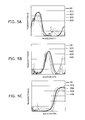
- FIGS. 3A to 3C are schematic graphs illustrating the effects of an incident angle ⁇ of the light on the characteristics of the color filters.
- FIG. 3A is the case of the light of the blue band
- FIG. 3B is the case of the light of the green band
- FIG. 3C is the case of the light of the red band.
- B 0 , G 0 , and R 0 are the case where the incident angle ⁇ is 0°;
- B 10 , G 10 , and R 10 are the case where the incident angle ⁇ is 10°
- B 20 , G 20 , and R 20 are the case where the incident angle ⁇ is 20°;
- B 30 , G 30 , and R 30 are the case where the incident angle ⁇ is 30°;
- B 40 , G 40 , and R 40 are the case where the incident angle ⁇ is 40°.
- the incident angle ⁇ is the angle between a direction (the Z direction) perpendicular to the major surface of the substrate 10 and the direction of the incident light. For example, in the case where the incident angle ⁇ is 0°, the light is incident from a direction perpendicular to the major surface of the substrate 10 .
- the transmittance was determined by a simulation using RCWA (Rigorous Coupled Wave Analysis).
- the wavelength at which the transmittance is a maximum changes as the incident angle ⁇ of the light changes.
- color shift occurs as the incident angle ⁇ of the light changes. This becomes pronounced as the incident angle ⁇ increases.
- the multiple components are provided in the periodic structure units 31 B, 31 G, and 31 R at different periods according to the incident angle of the light.
- the incident angle of the light that is incident on a region on the circumferential edge side of the substrate 10 is greater than the incident angle of the light that is incident on a region on the central side of the substrate 10 (corresponding to an example of the first region). Therefore, the periodicities of the multiple components of the periodic structure units 31 B, 31 G, and 31 R provided above the region on the central side of the substrate 10 are different from the periodicities of the multiple components of the periodic structure units 31 B, 31 G, and 31 R provided above the region on the circumferential edge side of the substrate 10 .
- the periods of the multiple components provided above the region on the circumferential edge side of the substrate 10 , for which the incident angle of the light is greater than that of the region on the central side of the substrate 10 are less than the periods of the multiple components provided above the region on the central side of the substrate 10 .
- FIG. 4 is a schematic view illustrating the case where the periodicity of the multiple components of the periodic structure units is changed according to the region of the substrate.
- the periodic structure units include multiple components having dot configurations.
- the multiple components 31 a having circular columnar configurations are disposed periodically in the periodic structure unit 311 provided above the region on the central side of the substrate 10 .
- Multiple components 31 a 1 having circular columnar configurations are disposed periodically in a periodic structure unit 311 a provided above the region on the circumferential edge side of the substrate 10 .
- the period is different between the multiple components 31 a and the multiple components 31 a 1 .
- a disposition pitch dimension P 1 of the multiple components 31 a 1 is less than a disposition pitch dimension P of the multiple components 31 a .
- the size of the multiple components 31 a 1 is smaller than the size of the multiple components 31 a.
- the disposition pitch dimension P of the multiple components 31 a is 0.17 ⁇ 0.2 ⁇ m at the color filter 20 B, 0.25 ⁇ 0.2 ⁇ m at the color filter 20 G, and not less than 0.15 ⁇ m and not more than 0.35 ⁇ m at the color filter 20 R.
- the disposition pitch dimension P 1 of the multiple components 31 a 1 may satisfy the following Formula (2).
- P 1 P ⁇ cos ⁇ (2) where P 1 is the disposition pitch dimension of the multiple components 31 a 1 , P is the disposition pitch dimension of the multiple components 31 a , and ⁇ is the incident angle of the light.
- Formula (2) also can be applied to the case where the periodic structure units include the multiple components 31 c having stripe configurations and the case where the periodic structure units include the multiple components 31 b having hole configurations.
- FIGS. 5A to 5C are schematic graphs illustrating effects of changing the periodicity of the multiple components of the periodic structure units according to the region of the substrate. Namely, these graphs are schematic graphs illustrating the effect of the case illustrated in FIG. 4 .
- FIG. 5A is the case of the light of the blue band
- FIG. 5B is the case of the light of the green band
- FIG. 5C is the case of the light of the red band.
- B 0 , G 0 , and R 0 are the case where the incident angle ⁇ is 0°;
- B 10 , G 10 , and R 10 are the case where the incident angle ⁇ is 10°;
- B 20 , G 20 , and R 20 are the case where the incident angle ⁇ is 20°;
- B 30 , G 30 , and R 30 are the case where the incident angle ⁇ is 30°;
- B 40 , G 40 , and R 40 are the case where the incident angle ⁇ is 40°.
- the incident angle ⁇ is the angle between the direction (the Z direction) perpendicular to the major surface of the substrate 10 and the direction of the incident light. For example, in the case where the incident angle ⁇ is 0°, the light is incident from the direction perpendicular to the major surface of the substrate 10 .
- the transmittance was determined by a simulation using RCWA.
- the change of the wavelength at which the transmittance is a maximum due to the change of the incident angle ⁇ of the light can be suppressed.
- the occurrence of the color shift due to the change of the incident angle ⁇ of the light can be suppressed.
- the periodic structure unit 313 includes the multiple components 31 c having stripe configurations disposed periodically, the periodicity is different according to the incident direction of the light.
- FIGS. 6A and 6B are schematic views illustrating the relationship between the incident direction of the light and the periodicity.
- FIG. 6A is the case where a disposition direction Sb of the multiple components 31 c having stripe configurations is parallel to the direction of a component Lxy of incident light L in a direction parallel to the major surface of the substrate 10 .
- this is the case where the direction of the component Lxy of the incident light L is orthogonal to the direction in which the multiple components 31 c having stripe configurations extend.
- FIG. 6B is the case where a disposition direction Sa of the multiple components 31 c having stripe configurations is orthogonal to the direction of the component Lxy of the incident light L in the direction parallel to the major surface of the substrate 10 .
- this is the case where the direction of the component Lxy of the incident light L is parallel to the direction in which the multiple components 31 c having stripe configurations extend.
- the periodic structure unit 313 has periodicity with respect to the direction of the component Lxy of the incident light L.
- the size of the component Lxy changes as the incident angle ⁇ of the incident light L changes. Therefore, in FIG. 6A , there is a risk that the suppression effect of the color shift may decrease because the resonance effect changes with the incident angle ⁇ .
- the periodic structure unit 313 does not have periodicity with respect to the direction of the component Lxy of the incident light L.
- the size of the component Lxy changes as the incident angle ⁇ of the incident light L changes.
- the resonance effect does not change even when the size of the component Lxy changes because the periodic structure unit 313 does not have periodicity with respect to the direction of the component Lxy of the incident light L. Therefore, in FIG. 6B , there is little risk that the suppression effect of the color shift may decrease even when the incident angle ⁇ changes.
- FIG. 7 is a schematic graph illustrating the effect of the case illustrated in FIG. 6B .
- FIG. 7 is the case of the light of the green band; GO is the case where the incident angle ⁇ is 0°; G 10 is the case where the incident angle ⁇ is 10°; G 20 is the case where the incident angle ⁇ is 20°; and G 30 is the case where the incident angle ⁇ is 30°.
- the incident angle ⁇ is the angle between the direction (the Z direction) perpendicular to the major surface of the substrate 10 and the direction of the incident light. For example, in the case where the incident angle ⁇ is 0°, the light is incident from the direction perpendicular to the major surface of the substrate 10 .
- the transmittance was determined by a simulation using RCWA.
- the change of the wavelength at which the transmittance is a maximum due to the change of the incident angle ⁇ of the light can be suppressed more than in the case illustrated in FIG. 5B .
- the occurrence of the color shift due to the change of the incident angle ⁇ of the light can be suppressed more than in the case illustrated in FIG. 5B .
- the multiple components 31 c having stripe configurations extend from the central side of the substrate 10 toward the circumferential edge side of the substrate 10 when viewed in plan such that the periodic structure unit 313 does not have periodicity with respect to the direction of the component Lxy of the incident light L.
- FIG. 8 is a schematic view illustrating the disposition form of the multiple components 31 c having stripe configurations.
- the periodic structure unit 313 does not have periodicity with respect to the direction of the component Lxy of the incident light L by using a disposition in which the multiple components 31 c having stripe configurations extend from the central side of the substrate 10 toward the circumferential edge side of the substrate 10 when viewed in plan. Therefore, the occurrence of the color shift due to the change of the incident angle ⁇ of the light can be suppressed further.
- FIG. 9 to FIG. 11 are schematic views illustrating other disposition forms of the multiple components 31 c having stripe configurations.
- FIG. 9 to FIG. 11 are schematic views illustrating the case where a region 60 where the color filters 20 B, 20 G, and 20 R are provided is subdivided; and the appropriate periodic structure units are provided in each of subdivided regions.
- FIG. 9 to FIG. 11 are the case where the color filters 20 B, 20 G, and 20 R are arranged in a Bayer arrangement.
- FIG. 9 is the case where the region 60 where the color filters 20 B, 20 G, and 20 R are provided is subdivided into 9 portions.
- the multiple components 31 c having stripe configurations provided in the periodic structure units 31 B, 31 G, and 31 R of the color filters 20 B, 20 G, and 20 R are provided to have designated periodicities for the transmitted wavelengths.
- the light of the designated wavelength bands can be guided into the photodiodes because the light other than the designated wavelength bands is reflected and absorbed.
- the disposition pitch dimensions of the multiple components 31 c having stripe configurations and/or the multiple components 31 d having dot configurations decrease toward the circumferential edge of the region 60 .
- the disposition pitch dimension of the multiple components 31 c and/or the disposition pitch dimension of the multiple components 31 d decreasing toward the circumferential edge of the region 60 the increase of the color shift can be suppressed even in the case where the incident angle ⁇ of the light increases.
- the increase of the color shift can be further suppressed by a configuration such as that recited below.
- a disposition is used in which the multiple components 31 c having stripe configurations extend from the central side of the region 60 (the substrate 10 ) toward the circumferential edge side of the region 60 (the substrate 10 ) when viewed in plan.
- a disposition is used in which the multiple components 31 c having stripe configurations of the regions 60 a and 60 c extend in a direction perpendicular to the edge of the region 60 .
- a disposition is used in which the multiple components 31 c having stripe configurations extend in a direction parallel to the diagonal line of the region 60 .
- the periodicity of the periodic structure units with respect to the direction of the component Lxy of the incident light L can be reduced. Therefore, the occurrence of the color shift due to the change of the incident angle ⁇ of the light can be suppressed further.
- the multiple components 31 d having dot configurations are provided in the region 60 d which is the region on the central side of the region 60 (the substrate 10 ). In such a case, in the region 60 d as well, a disposition may be used in which the multiple components 31 c having stripe configurations extend from the central side of the region 60 toward the circumferential edge side of the region 60 .
- the manufacturing of the periodic structure units 31 B, 31 G, and 31 R becomes difficult in the case where the multiple components 31 c having stripe configurations are provided in the region 60 d which is a region on the central side.
- the manufacturing of the periodic structure units 31 B, 31 G, and 31 R can be easy in the case where the multiple components 31 d having dot configurations are provided in the region 60 d.
- the multiple components 31 d having dot configurations are provided in the region 60 d to make the manufacturing of the periodic structure units 31 B, 31 G, and 31 R easy.
- FIG. 10 is the case where the region 60 where the color filters 20 B, 20 G, and 20 R are provided is subdivided into 4 portions.
- FIG. 10 is the case where the subdivision into 4 portions is performed by diagonal lines 601 of the region 60 .
- the multiple components 31 c having stripe configurations provided in the periodic structure units 31 B, 31 G, and 31 R of the color filters 20 B, 20 G, and 20 R are provided to have the designated periodicities for the transmitted wavelengths.
- the disposition pitch dimension of the multiple components 31 c decreases toward the circumferential edge of the region 60 .
- a disposition is used in which the multiple components 31 c having stripe configurations extend from the central side of the region 60 (the substrate 10 ) toward the circumferential edge side of the region 60 (the substrate 10 ) when viewed in plan.
- a disposition is used in which the multiple components 31 c having stripe configurations extend in the direction perpendicular to the edge of the region 60 .
- a disposition of the multiple components 31 c similar to that of the region 60 b illustrated in FIG. 9 may be used proximally to the diagonal line 601 .
- the manufacturing of the periodic structure units 31 B, 31 G, and 31 R becomes difficult.
- the disposition of the multiple components 31 c is similar within each of the regions 60 a 1 and 60 c 1 , the manufacturing of the periodic structure units 31 B, 31 G, and 31 R can be easy.
- the disposition of the multiple components 31 c is similar within each of the regions 60 a 1 and 60 c 1 to make the manufacturing of the periodic structure units 31 B, 31 G, and 31 R easy.
- FIG. 11 is the case where the region 60 where the color filters 20 B, 20 G, and 20 R are provided is subdivided into 8 portions.
- the multiple components 31 c having stripe configurations provided in the periodic structure units 31 B, 31 G, and 31 R of the color filters 20 B, 20 G, and 20 R are provided to have the designated periodicities for the transmitted wavelengths.
- the disposition pitch dimension of the multiple components 31 c decreases toward the circumferential edge of the region 60 .
- the disposition is used in which the multiple components 31 c having stripe configurations extend from the central side of the region 60 (the substrate 10 ) toward the circumferential edge side of the region 60 (the substrate 10 ) when viewed in plan.
- a disposition is used in which the multiple components 31 c having stripe configurations extend in the direction perpendicular to the edge of the region 60 .
- a disposition is used in which the multiple components 31 c having stripe configurations extend in the direction parallel to the diagonal line of the region 60 .
- the manufacturing of the periodic structure units 31 B, 31 G, and 31 R becomes difficult.
- the manufacturing of the periodic structure units 31 B, 31 G, and 31 R can be easy in the case where the disposition of the multiple components 31 c has the same configuration within each of the subdivided regions.
- the periodicity of the periodic structure units with respect to the direction of the component Lxy of the incident light L can be reduced if the multiple components 31 c extend from the central side of the region 60 (the substrate 10 ) toward the circumferential edge side of the region 60 (the substrate 10 ). Therefore, the occurrence of the color shift due to the change of the incident angle ⁇ of the light can be suppressed.
- FIG. 12 to FIG. 14 are schematic cross-sectional views illustrating solid-state imaging elements according to other embodiments.
- the color filters 20 B, 20 G, and 20 R may be provided on the substrate 10 ; and the interconnect layer 13 may be provided on the color filters 20 B, 20 G, and 20 R.
- the microlenses 51 are provided on the interconnect layer 13 .
- the periodic structure units 31 B, 31 G, and 31 R of the color filters 20 B, 20 G, and 20 R are provided on the substrate 10 ; and the stacked structure units 21 B, 21 G, and 21 R are provided on the periodic structure units 31 B, 31 G, and 31 R.
- the periodic structure units 31 B, 31 G, and 31 R may be provided on the substrate 10 ; and the interconnect layer 13 may be provided on the periodic structure units 31 B, 31 G, and 31 R.
- the stacked structure units 21 B, 21 G, and 21 R are provided on the interconnect layer 13 .
- the microlenses 51 are provided on the stacked structure units 21 B, 21 G, and 21 R.
- a so-called back-side illuminated structure may be used.
- the periodic structure units 31 B, 31 G, and 31 R may be provided on the substrate 10 ; and the stacked structure units 21 B, 21 G, and 21 R may be provided on the periodic structure units 31 B, 31 G, and 31 R.
- the microlenses 51 are provided on the stacked structure units 21 B, 21 G, and 21 R.
- the suppression of the color shift can be realized by providing the periodic structure units described above.
- the periodic structure units 31 B, 31 G, and 31 R are provided on the substrate 10 .
- the cost can be reduced by reducing the number of processes because the periodic structure units 31 B, 31 G, and 31 R can be formed simultaneously with the gate electrodes of the transistors of the peripheral circuit, etc.
- a solid-state imaging element that can suppress the color shift can be realized.
Abstract
Description
D=λ/(4×n) (1)
where D is the film thickness of the
P1=P·cos θ (2)
where P1 is the disposition pitch dimension of the
Claims (20)
P1=P·cos θ
D=λ/(4×n)
Applications Claiming Priority (2)
| Application Number | Priority Date | Filing Date | Title |
|---|---|---|---|
| JP2011-191903 | 2011-09-02 | ||
| JP2011191903A JP5337212B2 (en) | 2011-09-02 | 2011-09-02 | Solid-state image sensor |
Publications (2)
| Publication Number | Publication Date |
|---|---|
| US20130057738A1 US20130057738A1 (en) | 2013-03-07 |
| US8890984B2 true US8890984B2 (en) | 2014-11-18 |
Family
ID=47752876
Family Applications (1)
| Application Number | Title | Priority Date | Filing Date |
|---|---|---|---|
| US13/585,113 Expired - Fee Related US8890984B2 (en) | 2011-09-02 | 2012-08-14 | Solid-state imaging element |
Country Status (4)
| Country | Link |
|---|---|
| US (1) | US8890984B2 (en) |
| JP (1) | JP5337212B2 (en) |
| KR (1) | KR101315537B1 (en) |
| CN (1) | CN102983142A (en) |
Cited By (1)
| Publication number | Priority date | Publication date | Assignee | Title |
|---|---|---|---|---|
| US10840302B2 (en) | 2016-03-30 | 2020-11-17 | Samsung Electronics Co., Ltd. | Image sensor including nanostructure color filter |
Families Citing this family (17)
| Publication number | Priority date | Publication date | Assignee | Title |
|---|---|---|---|---|
| JP5364743B2 (en) * | 2011-03-01 | 2013-12-11 | 株式会社東芝 | Semiconductor device |
| JP2015037095A (en) * | 2013-08-12 | 2015-02-23 | 株式会社東芝 | Solid state image pickup device |
| JP2015179731A (en) * | 2014-03-19 | 2015-10-08 | 株式会社東芝 | Solid state imaging apparatus |
| CN105206630A (en) * | 2014-06-18 | 2015-12-30 | 上海华力微电子有限公司 | CMOS photosensitive element and preparation method |
| FR3025361B1 (en) * | 2014-08-29 | 2017-12-08 | Commissariat Energie Atomique | PHOTOSENSITIVE SENSOR |
| KR102313989B1 (en) * | 2014-09-30 | 2021-10-15 | 삼성전자주식회사 | Image sensor and electronic device including the same |
| KR102360074B1 (en) * | 2014-11-28 | 2022-02-08 | 삼성전자주식회사 | Image sensor including nanostructure color filter |
| KR102654861B1 (en) * | 2016-03-30 | 2024-04-05 | 삼성전자주식회사 | Image sensor including nanostructure color filter |
| JP2018026378A (en) * | 2016-08-08 | 2018-02-15 | ソニーセミコンダクタソリューションズ株式会社 | Solid state imaging device and manufacturing method, and electronic apparatus |
| US10983339B2 (en) * | 2016-08-09 | 2021-04-20 | Sony Corporation | Solid-state imaging element, pupil correction method for solid-state imaging element, imaging device, and information processing device |
| WO2019124562A1 (en) * | 2017-12-22 | 2019-06-27 | ソニーセミコンダクタソリューションズ株式会社 | Solid-state imaging device and electronic device |
| US10916575B2 (en) | 2018-04-04 | 2021-02-09 | Samsung Electronics Co., Ltd. | Image sensor and method of manufacturing image sensor |
| CN109683379A (en) * | 2019-01-25 | 2019-04-26 | 京东方科技集团股份有限公司 | Color membrane structure, color membrane substrates, display panel and display device |
| JP2021141264A (en) * | 2020-03-09 | 2021-09-16 | ソニーセミコンダクタソリューションズ株式会社 | Solid-state imaging element and electronic device |
| WO2021186908A1 (en) * | 2020-03-17 | 2021-09-23 | ソニーセミコンダクタソリューションズ株式会社 | Solid-state imaging device |
| DE102020118842A1 (en) | 2020-07-16 | 2022-01-20 | Fraunhofer-Gesellschaft zur Förderung der angewandten Forschung eingetragener Verein | Optical filter with nanostructured layers and spectral sensor with such layers |
| US11317039B1 (en) * | 2021-01-06 | 2022-04-26 | Visera Technologies Company Limited | Image-sensing device |
Citations (11)
| Publication number | Priority date | Publication date | Assignee | Title |
|---|---|---|---|---|
| US20060164720A1 (en) * | 2005-01-24 | 2006-07-27 | Matsushita Electric Industrial Co., Ltd. | Multilayer interference filter, manufacturing method for multilayer interference filter, solid-state imaging device and camera |
| US20060205107A1 (en) * | 2004-01-15 | 2006-09-14 | Yuuichi Inaba | Solid-state imaging device, manufacturing method of solid-state imaging device, and camera employing same |
| US20070058055A1 (en) * | 2003-08-01 | 2007-03-15 | Takumi Yamaguchi | Solid-state imaging device, manufacturing method for solid-state imaging device, and camera using the same |
| US20070235756A1 (en) * | 2006-04-10 | 2007-10-11 | Matsushita Electric Industrial Co., Ltd. | Solid-state imaging device, camera and signal processing method |
| JP2008170979A (en) | 2006-12-13 | 2008-07-24 | Matsushita Electric Ind Co Ltd | Solid-state imaging apparatus, manufacturing method therefor and camera |
| US7420610B2 (en) * | 2004-12-15 | 2008-09-02 | Matsushita Electric Industrial Co., Ltd. | Solid-state imaging element, solid-state imaging device, and method for fabricating the same |
| US20080251873A1 (en) * | 2006-12-13 | 2008-10-16 | Matsushita Electric Industrial Co., Ltd. | Solid-state imaging device, manufactoring method thereof and camera |
| US20090039340A1 (en) * | 2004-12-10 | 2009-02-12 | Sony Corporation | Method and apparatus for acquiring physical information, method for manufacturing semiconductor device including array of a plurality of unit components for detecting physical quantity distribution, light-receiving device and manufacturing method therefor, and solid-state imaging device and manufacturing method therefor |
| JP2010225944A (en) | 2009-03-24 | 2010-10-07 | Toshiba Corp | Solid-state imaging device |
| US20110043823A1 (en) * | 2006-08-09 | 2011-02-24 | Hartmut Hillmer | Optical filter and method for the production of the same, and device for the examination of electromagnetic radiation |
| US20110128423A1 (en) * | 2009-12-02 | 2011-06-02 | Lee Myung-Bok | Image sensor and method of manufacturing the same |
Family Cites Families (5)
| Publication number | Priority date | Publication date | Assignee | Title |
|---|---|---|---|---|
| JP5051817B2 (en) * | 2006-06-21 | 2012-10-17 | Agcテクノグラス株式会社 | Visibility correction filter glass and visibility correction filter |
| JP5017193B2 (en) * | 2008-06-30 | 2012-09-05 | パナソニック株式会社 | Solid-state imaging device and camera |
| JP4770928B2 (en) * | 2009-01-13 | 2011-09-14 | ソニー株式会社 | Optical element and solid-state image sensor |
| JP2010251489A (en) * | 2009-04-15 | 2010-11-04 | Sony Corp | Solid-state imaging device and electronic apparatus |
| JP2010282992A (en) * | 2009-06-02 | 2010-12-16 | Sony Corp | Solid-state imaging device and method of manufacturing the same, and electronic apparatus |
-
2011
- 2011-09-02 JP JP2011191903A patent/JP5337212B2/en not_active Expired - Fee Related
-
2012
- 2012-08-14 US US13/585,113 patent/US8890984B2/en not_active Expired - Fee Related
- 2012-08-29 CN CN2012103132696A patent/CN102983142A/en active Pending
- 2012-08-30 KR KR1020120095333A patent/KR101315537B1/en not_active IP Right Cessation
Patent Citations (11)
| Publication number | Priority date | Publication date | Assignee | Title |
|---|---|---|---|---|
| US20070058055A1 (en) * | 2003-08-01 | 2007-03-15 | Takumi Yamaguchi | Solid-state imaging device, manufacturing method for solid-state imaging device, and camera using the same |
| US20060205107A1 (en) * | 2004-01-15 | 2006-09-14 | Yuuichi Inaba | Solid-state imaging device, manufacturing method of solid-state imaging device, and camera employing same |
| US20090039340A1 (en) * | 2004-12-10 | 2009-02-12 | Sony Corporation | Method and apparatus for acquiring physical information, method for manufacturing semiconductor device including array of a plurality of unit components for detecting physical quantity distribution, light-receiving device and manufacturing method therefor, and solid-state imaging device and manufacturing method therefor |
| US7420610B2 (en) * | 2004-12-15 | 2008-09-02 | Matsushita Electric Industrial Co., Ltd. | Solid-state imaging element, solid-state imaging device, and method for fabricating the same |
| US20060164720A1 (en) * | 2005-01-24 | 2006-07-27 | Matsushita Electric Industrial Co., Ltd. | Multilayer interference filter, manufacturing method for multilayer interference filter, solid-state imaging device and camera |
| US20070235756A1 (en) * | 2006-04-10 | 2007-10-11 | Matsushita Electric Industrial Co., Ltd. | Solid-state imaging device, camera and signal processing method |
| US20110043823A1 (en) * | 2006-08-09 | 2011-02-24 | Hartmut Hillmer | Optical filter and method for the production of the same, and device for the examination of electromagnetic radiation |
| JP2008170979A (en) | 2006-12-13 | 2008-07-24 | Matsushita Electric Ind Co Ltd | Solid-state imaging apparatus, manufacturing method therefor and camera |
| US20080251873A1 (en) * | 2006-12-13 | 2008-10-16 | Matsushita Electric Industrial Co., Ltd. | Solid-state imaging device, manufactoring method thereof and camera |
| JP2010225944A (en) | 2009-03-24 | 2010-10-07 | Toshiba Corp | Solid-state imaging device |
| US20110128423A1 (en) * | 2009-12-02 | 2011-06-02 | Lee Myung-Bok | Image sensor and method of manufacturing the same |
Cited By (2)
| Publication number | Priority date | Publication date | Assignee | Title |
|---|---|---|---|---|
| US10840302B2 (en) | 2016-03-30 | 2020-11-17 | Samsung Electronics Co., Ltd. | Image sensor including nanostructure color filter |
| US11968848B2 (en) | 2016-03-30 | 2024-04-23 | Samsung Electronics Co., Ltd. | Image sensor including nanostructure color filter |
Also Published As
| Publication number | Publication date |
|---|---|
| KR20130025823A (en) | 2013-03-12 |
| US20130057738A1 (en) | 2013-03-07 |
| CN102983142A (en) | 2013-03-20 |
| JP5337212B2 (en) | 2013-11-06 |
| JP2013055202A (en) | 2013-03-21 |
| KR101315537B1 (en) | 2013-10-08 |
Similar Documents
| Publication | Publication Date | Title |
|---|---|---|
| US8890984B2 (en) | Solid-state imaging element | |
| JP5534981B2 (en) | Solid-state imaging device | |
| JP5372102B2 (en) | Photoelectric conversion device and imaging system | |
| US8670051B2 (en) | Solid-state image sensor and camera having improved sensitivity and color separation characteristics | |
| JP6055270B2 (en) | Solid-state imaging device, manufacturing method thereof, and camera | |
| US8330840B2 (en) | Image sensor with multilayer interference filters | |
| US8759929B2 (en) | Solid-state imaging device | |
| US8970768B2 (en) | Unit pixel array and image sensor having the same | |
| US9117717B2 (en) | Solid-state image pickup device having a multilayer interference filter including an upper laminated structure, a control structure and lower laminated structure | |
| US8823123B2 (en) | Solid-state image sensor | |
| WO2012004934A1 (en) | Solid state imaging device | |
| US20130093034A1 (en) | Solid-state imaging device and manufacturing method of solid-state imaging device | |
| JP2012064824A (en) | Solid state image sensor, method of manufacturing the same, and camera | |
| JP2013038091A (en) | Solid-state image sensor and manufacturing method therefor | |
| JP2014130890A (en) | Photoelectric conversion device | |
| US8294796B2 (en) | Image sensor | |
| US8542311B2 (en) | Multisection light guides for image sensor pixels | |
| JP2008177362A (en) | Solid-state imaging apparatus and camera | |
| US20230197746A1 (en) | Image sensor | |
| JP2011061134A (en) | Semiconductor image sensor | |
| US11699768B1 (en) | Patterned electrode structure for image sensor | |
| JP2011243785A (en) | Solid state imaging device | |
| JP2006344755A (en) | Solid state imaging device and camera employing it | |
| KR20070021430A (en) | Image sensor with decreased signal noise and method for manufacturing the same | |
| JP2011009311A (en) | Solid-state image sensor and method of manufacturing the same |
Legal Events
| Date | Code | Title | Description |
|---|---|---|---|
| AS | Assignment |
Owner name: KABUSHIKI KAISHA TOSHIBA, JAPAN Free format text: ASSIGNMENT OF ASSIGNORS INTEREST;ASSIGNORS:KONNO, YUSAKU;OKADA, NAOTADA;KOKUBUN, KOICHI;SIGNING DATES FROM 20120704 TO 20120706;REEL/FRAME:028784/0504 |
|
| FEPP | Fee payment procedure |
Free format text: PAYOR NUMBER ASSIGNED (ORIGINAL EVENT CODE: ASPN); ENTITY STATUS OF PATENT OWNER: LARGE ENTITY |
|
| FEPP | Fee payment procedure |
Free format text: MAINTENANCE FEE REMINDER MAILED (ORIGINAL EVENT CODE: REM.) |
|
| LAPS | Lapse for failure to pay maintenance fees |
Free format text: PATENT EXPIRED FOR FAILURE TO PAY MAINTENANCE FEES (ORIGINAL EVENT CODE: EXP.); ENTITY STATUS OF PATENT OWNER: LARGE ENTITY |
|
| STCH | Information on status: patent discontinuation |
Free format text: PATENT EXPIRED DUE TO NONPAYMENT OF MAINTENANCE FEES UNDER 37 CFR 1.362 |
|
| FP | Lapsed due to failure to pay maintenance fee |
Effective date: 20181118 |