US8885363B2 - Dual-mode switching power control device - Google Patents
Dual-mode switching power control device Download PDFInfo
- Publication number
- US8885363B2 US8885363B2 US14/049,301 US201314049301A US8885363B2 US 8885363 B2 US8885363 B2 US 8885363B2 US 201314049301 A US201314049301 A US 201314049301A US 8885363 B2 US8885363 B2 US 8885363B2
- Authority
- US
- United States
- Prior art keywords
- power
- loading
- driving controller
- dual
- control device
- Prior art date
- Legal status (The legal status is an assumption and is not a legal conclusion. Google has not performed a legal analysis and makes no representation as to the accuracy of the status listed.)
- Expired - Fee Related
Links
Images


Classifications
-
- H—ELECTRICITY
- H02—GENERATION; CONVERSION OR DISTRIBUTION OF ELECTRIC POWER
- H02M—APPARATUS FOR CONVERSION BETWEEN AC AND AC, BETWEEN AC AND DC, OR BETWEEN DC AND DC, AND FOR USE WITH MAINS OR SIMILAR POWER SUPPLY SYSTEMS; CONVERSION OF DC OR AC INPUT POWER INTO SURGE OUTPUT POWER; CONTROL OR REGULATION THEREOF
- H02M3/00—Conversion of dc power input into dc power output
- H02M3/22—Conversion of dc power input into dc power output with intermediate conversion into ac
- H02M3/24—Conversion of dc power input into dc power output with intermediate conversion into ac by static converters
- H02M3/28—Conversion of dc power input into dc power output with intermediate conversion into ac by static converters using discharge tubes with control electrode or semiconductor devices with control electrode to produce the intermediate ac
- H02M3/325—Conversion of dc power input into dc power output with intermediate conversion into ac by static converters using discharge tubes with control electrode or semiconductor devices with control electrode to produce the intermediate ac using devices of a triode or a transistor type requiring continuous application of a control signal
- H02M3/335—Conversion of dc power input into dc power output with intermediate conversion into ac by static converters using discharge tubes with control electrode or semiconductor devices with control electrode to produce the intermediate ac using devices of a triode or a transistor type requiring continuous application of a control signal using semiconductor devices only
- H02M3/33507—Conversion of dc power input into dc power output with intermediate conversion into ac by static converters using discharge tubes with control electrode or semiconductor devices with control electrode to produce the intermediate ac using devices of a triode or a transistor type requiring continuous application of a control signal using semiconductor devices only with automatic control of the output voltage or current, e.g. flyback converters
- H02M3/33523—Conversion of dc power input into dc power output with intermediate conversion into ac by static converters using discharge tubes with control electrode or semiconductor devices with control electrode to produce the intermediate ac using devices of a triode or a transistor type requiring continuous application of a control signal using semiconductor devices only with automatic control of the output voltage or current, e.g. flyback converters with galvanic isolation between input and output of both the power stage and the feedback loop
-
- H—ELECTRICITY
- H02—GENERATION; CONVERSION OR DISTRIBUTION OF ELECTRIC POWER
- H02M—APPARATUS FOR CONVERSION BETWEEN AC AND AC, BETWEEN AC AND DC, OR BETWEEN DC AND DC, AND FOR USE WITH MAINS OR SIMILAR POWER SUPPLY SYSTEMS; CONVERSION OF DC OR AC INPUT POWER INTO SURGE OUTPUT POWER; CONTROL OR REGULATION THEREOF
- H02M1/00—Details of apparatus for conversion
- H02M1/0003—Details of control, feedback or regulation circuits
- H02M1/0032—Control circuits allowing low power mode operation, e.g. in standby mode
-
- H02M2001/0032—
-
- Y—GENERAL TAGGING OF NEW TECHNOLOGICAL DEVELOPMENTS; GENERAL TAGGING OF CROSS-SECTIONAL TECHNOLOGIES SPANNING OVER SEVERAL SECTIONS OF THE IPC; TECHNICAL SUBJECTS COVERED BY FORMER USPC CROSS-REFERENCE ART COLLECTIONS [XRACs] AND DIGESTS
- Y02—TECHNOLOGIES OR APPLICATIONS FOR MITIGATION OR ADAPTATION AGAINST CLIMATE CHANGE
- Y02B—CLIMATE CHANGE MITIGATION TECHNOLOGIES RELATED TO BUILDINGS, e.g. HOUSING, HOUSE APPLIANCES OR RELATED END-USER APPLICATIONS
- Y02B70/00—Technologies for an efficient end-user side electric power management and consumption
- Y02B70/10—Technologies improving the efficiency by using switched-mode power supplies [SMPS], i.e. efficient power electronics conversion e.g. power factor correction or reduction of losses in power supplies or efficient standby modes
Definitions
- the present invention relates to a control device for power conversion, and more specifically to a dual-mode switching power control device that dynamically controls a flyback converter to perform DCM (Discontinuous Conduction Mode) or CCM (Continuous Conduction Mode) based on a loading state.
- DCM Continuous Conduction Mode
- CCM Continuous Conduction Mode
- ICs integrated circuits
- electric motors need 12V DC
- high power devices require 110V or 220V AC, like city power.
- the lamp of the LED display usually operates at even much higher voltage.
- many kinds of electric converters have been developed to meet those various demands.
- flyback converters which have advantages of simple architecture and wider range of adjustable voltage, are one of the most used switching power converters. As a result, flyback converters are often applied to electronic products consuming medium or small power. Specifically, flyback converters employ switching elements to control the current flowing through the electric transformer so as to generate the output power as desired. At the same time, passive resistor capacitor diodes (RCD) are used to reduce the voltage stress of the switching elements and effectively absorb voltage surge generated by the electric transformer due to leakage inductance.
- RCD passive resistor capacitor diodes
- QR Quasi-Resonant
- DCM Discontinuous Conduction Mode
- EMI electromagnetic interference
- CCM Continuous Conduction Mode
- QR flyback converters operating in DCM are not suitable for higher power applications.
- current power converters use various fixed preset modes or only one mode as the operating mode, and it is not possible to adjust or change the operating mode or operating parameters for different electric transformers and other elements such that the best efficiency is attained.
- dual-mode switching power control device which is implemented by digital design and applicable from light to heavy loading, in particular can automatically determine the loading state and dynamically switch to DCM or CCM based on the loading state so as to improve the efficiency of power conversion, thereby overcoming the above problems in the prior arts.
- the primary objective of the present invention is to provide dual-mode switching power control device for converting an input power with an input voltage into an output power with an output voltage supplied to an external load.
- the dual-mode switching power control device of the present invention generally includes an electric transformer, a PWM driving controller, a switching transistor, an isolation element, an output diode and an output capacitor.
- the electric transformer, the PWM driving controller, the switching transistor and the input power form a driving control loop
- the electric transformer, the output diode, the output capacitor and the isolation element form a feedback loop for generating a feedback signal which is transmitted to the PWM driving controller.
- the PWM driving controller determines the loading state based on the feedback signal. Specifically, the PWM driving controller selects DCM to perform in case of light loading, and CCM is determined in case of heavy loading such that the switching transistor is driven to control the current flowing through the electric transformer, and the function of power conversion from the input power into output power is achieved.
- the present invention can reduce the switching loss by performing DCM in light loading, and reduce the conduction loss by performing CCM in heavy loading so as to greatly improve the efficiency of power conversion and is suitable for higher power applications.
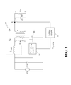
- FIG. 1 is a schematic view illustrating the dual-mode switching power control device according to the present invention
- FIG. 2 is a view showing the turn-on operation for the switching element of the dual-mode switching power control device according to the one embodiment of the present invention
- FIG. 3 is a view showing the turn-off operation for the switching element of the dual-mode switching power control device according to the present invention
- FIG. 4 is a diagram illustrating the conversion efficiency of the dual-mode switching power control device with the input power of 110V according to the present invention.
- FIG. 5 is a diagram illustrating the conversion efficiency of the dual-mode switching power control device with the input power of 220V according to the present invention.
- FIG. 1 illustrates a dual-mode switching power control device according to the present invention.
- the dual-mode switching power control device of the present invention generally includes a PWM (pulse width modulation) driving controller 10 , a switching transistor 20 , an electric transformer 30 , an isolation element 40 , an output diode D and an output capacitor Co.
- the present invention implements the function of converting an input power with an input voltage Vin into an output power with an output voltage Vo for supplying to an external load Ro. More specifically, the electric transformer 30 , the PWM driving controller 10 , the switching transistor 20 and the input power with the input voltage Vin form a driving control loop.
- the electric transformer 30 , the output diode D, the output capacitor Co and the isolation element 40 form a feedback loop for generating a feedback signal, like a feedback voltage V_comp shown in FIG. 1 .
- the external load Ro is connected to the output capacitor Co in parallel, and the terminal voltage of the output capacitor Co is the output voltage Vo of the output power.
- any electrical signal other than the feedback voltage V_comp can also be specified as the above feedback signal, such as the feedback current or power corresponding to the output power.
- the input power can be supplied with DC power, which is generated by rectifying common city power through an electric rectifying bridge.
- city power is 110V or 220V AC power
- the input power is 110V or 220V DC power.
- an input capacitor Cin is connected to the input power for stabilization.
- the PWM driving controller 10 is a single chip, which is selected from a group consisting of MCU (microcontroller) or CPU (central processing unit), or an electric circuit consisting of discrete electric components. That is, the PWM driving controller 10 is implemented by digital design.
- the switching transistor 20 may include a power transistor, like a MOSFET (metal-oxide-semiconductor field effect transistor), and the isolation element 40 may include a photo coupler or an electric circuit consisting of at least one passive element, such as a resistor and a capacitor.
- MOSFET metal-oxide-semiconductor field effect transistor
- the feedback voltage V_comp is served as the feedback signal to describe the architecture and primary aspects of the dual-mode switching power control device according to the present invention.
- the electric transformer 30 includes a first side inductor Lp and a second side inductor Ls.
- the first side inductor Lp consists of a magnetizing inductor Lm and a leakage inductor Lleak connected in series.
- the magnetizing inductor Lm is used to couple the magnetic flux generated with the second side inductor Ls, and the leakage inductor Lleak is not coupled with the second side inductor Ls.
- One end of the first side inductor Lp is connected to the drain of the switching transistor 20 , the PWM driving controller 10 is connected to the gate of the drain of the switching transistor 20 , and the input voltage Vin of the input power is connected to the source of the switching transistor 20 and another end of the first side inductor Lp which is further connected to the PWM driving controller 10 .
- One end of the second side inductor Ls is connected to the positive end of the output diode D, and the negative end of the output diode D is connected to one end of the output capacitor Co and one end of the isolation element 40 .
- the isolation element 40 converts the output voltage Vo into the feedback signal, that is, the feedback voltage V_comp, which is then transmitted to the PWM driving controller 10 via another end of the isolation element 40 .
- the PWM driving controller 10 determines whether the current loading state of the load Ro is light loading or heavy loading. Specifically, the loading state is light loading when the feedback signal is smaller than a threshold value, and the loading state is heavy loading when the feedback signal is larger than the threshold value.
- the PWM driving controller 10 performs DCM to generate the PWM driving signal, which is transmitted to the gate of the switching transistor 20 to drive the switching transistor 20 .
- CCM is performed to drive the switching transistor 20 . Therefore, the present invention can dynamically select DCM or CCM according to the load state. Furthermore, in order to reduce EMI (electromagnetic interference), it is possible to include jitter design under CCM or DCM.
- FIG. 2 is a view showing the turn-on operation for the switching element of the dual-mode switching power control device according to the present invention
- FIG. 3 is a view showing the turn-off operation for the switching element of the dual-mode switching power control device according to the present invention.
- the PWM driving controller 10 is not shown for clear explanation.
- the PWM driving signal generated by the PWM driving controller 10 is used to drive the switching element 20 such that the switching element 20 is turned on to allow the current from the input power to flow through the first side inductor Lp of the electric transformer 30 and the switching element 20 , which form a current loop.
- a negative voltage is induced at the second side inductor Ls of the electric transformer 30 to turn off the output diode D such that the output capacitor Co discharges to the load Ro, that is, the load Ro is supplied by the output capacitor Co.
- the PWM driving controller 10 ceases the PWM driving signal to turn off the switching element 20 such that some residual current still flows through the first side inductor Lp and a positive voltage corresponding to the residual current in the first side inductor Lp is induced by the second side inductor Ls to turn on the output diode D.
- the second side inductor Ls thus supplies the desired power to the load Ro.
- the threshold value in the dual-mode switching power control device of the present invention is specified according to the efficiency of power conversion and can be optimized by measuring in experiments. For example, as shown in FIGS. 4 and 5 , the data are measured in experiments for the input power of 100 ⁇ 120V and 210 ⁇ 230V, respectively.
- the PWM driving controller first scan the whole system to acquire the characteristic CCM and DCM curves, and it is clearly seen that DCM has higher efficiency when the output power is lower, and CCM has higher efficiency when the output power is higher.
- the switching points for DCM or CCM are specified by the loading power or the output power of 50 W ⁇ 70 W and 90 W ⁇ 110 W for the input power of 100 ⁇ 120V and 210 ⁇ 230V, respectively.
- the present invention may also include other nonlinear forms to correlate the feedback signal with the loading power, such as polynomial, semi-logarithmic, exponential function, and trigonometric functions, or the lookup table derived from experimental data and stored in the PWM driving controller 10 .
- one feature of the present invention is that the feedback signal is used to determine the loading state such that DCM is performed when the output power is lower to reduce the switching loss, and CCM is performed when the output power is higher to reduce the conduction loss.
- the efficiency of power conversion is greatly improved and it is possible to apply to higher power electric or electronic devices.
- the dual-mode switching power control device is implemented by digital design and can thus automatically determine the current loading state and select CCM or DCM as the operating mode to perform.
- the system can always operate in only one operating mode, which is selected from CCM and DCM, by setting different parameters for switching frequency and duty.
- the various curves of conversion efficiency are first scanned, like FIGS. 4 and 5 , and the optimal curve with the best efficiency is then selected.
- the PWM driving controller is implemented by digital design, even at the same loading, it is possible to calculate the output power and adjust the optimal parameters to perform the best efficiency according to the set frequency and duty.
- the system with the output power of 18 W can respectively preset different frequency, duty, CCM/DCM at any loading between zero loading and full loading, such as zero loading (0 W), 1 ⁇ 4 loading (4.5 W), 1 ⁇ 2 loading (9 W), 3 ⁇ 4 loading (13.5 W) or full loading (18 W).
- the PWM driving controller may scan and measure the efficiency curve of power conversion corresponding to CCM/DCM selected, and select CCM or DCM with best efficiency as the target operating mode.
- the PWM driving controller 10 calculates the output power for the loading resulted from the external load Ro and then adjusts the optimal parameters to perform the best efficiency according to the set frequency and duty.
Landscapes
- Engineering & Computer Science (AREA)
- Power Engineering (AREA)
- Dc-Dc Converters (AREA)
Abstract
Description
V_comp=Vo*K
where K is a ratio constant, like 1/20 or 1/50. Certainly, the above-mentioned operations are only illustrative examples for showing the primary aspects of the present invention and not intended to limit the scope of the present invention. Thus, the present invention may also include other nonlinear forms to correlate the feedback signal with the loading power, such as polynomial, semi-logarithmic, exponential function, and trigonometric functions, or the lookup table derived from experimental data and stored in the
Claims (8)
Applications Claiming Priority (3)
| Application Number | Priority Date | Filing Date | Title |
|---|---|---|---|
| TW102100582A TWI542121B (en) | 2013-01-08 | 2013-01-08 | Dual - mode power supply switching control device |
| TW102100582U | 2013-01-08 | ||
| TW102100582 | 2013-01-08 |
Publications (2)
| Publication Number | Publication Date |
|---|---|
| US20140192563A1 US20140192563A1 (en) | 2014-07-10 |
| US8885363B2 true US8885363B2 (en) | 2014-11-11 |
Family
ID=51060818
Family Applications (1)
| Application Number | Title | Priority Date | Filing Date |
|---|---|---|---|
| US14/049,301 Expired - Fee Related US8885363B2 (en) | 2013-01-08 | 2013-10-09 | Dual-mode switching power control device |
Country Status (2)
| Country | Link |
|---|---|
| US (1) | US8885363B2 (en) |
| TW (1) | TWI542121B (en) |
Cited By (2)
| Publication number | Priority date | Publication date | Assignee | Title |
|---|---|---|---|---|
| KR20160080019A (en) * | 2014-12-29 | 2016-07-07 | 주식회사 효성 | Power control device for sub-module of mmc converter |
| US20160353532A1 (en) * | 2015-05-29 | 2016-12-01 | Linear Technology Corporation | Maintaining output capacitance voltage in led driver systems during pwm off times |
Families Citing this family (10)
| Publication number | Priority date | Publication date | Assignee | Title |
|---|---|---|---|---|
| US9496782B2 (en) * | 2011-12-22 | 2016-11-15 | B/E Aerospace, Inc. | Digitally-controlled power factor correction circuits, methods and articles of manufacture |
| TWI569563B (en) * | 2015-10-22 | 2017-02-01 | Multifunction Power Converter | |
| JP6707358B2 (en) * | 2016-02-12 | 2020-06-10 | ローム株式会社 | LCD backlight LED drive circuit, its control circuit, electronic equipment |
| US20170346405A1 (en) * | 2016-05-26 | 2017-11-30 | Inno-Tech Co., Ltd. | Dual-mode operation controller for flyback converter with primary-side regulation |
| EP3399636B1 (en) * | 2017-05-04 | 2020-02-12 | OSRAM GmbH | Electronic converter and related lighting system |
| KR20190068094A (en) | 2017-12-08 | 2019-06-18 | 삼성전자주식회사 | Semiconductor memory device and memory system |
| US11863079B2 (en) | 2021-06-30 | 2024-01-02 | Dialog Semiconductor Inc. | Switching power converter with secondary-side control |
| CN113991980A (en) * | 2021-12-24 | 2022-01-28 | 深圳市芯茂微电子有限公司 | Control method and controller of switching power supply and switching power supply |
| CN114415814A (en) * | 2021-12-28 | 2022-04-29 | 歌尔科技有限公司 | Control method, device and equipment of electronic equipment and readable storage medium |
| CN115333389A (en) * | 2022-08-12 | 2022-11-11 | 上海安世博能源科技有限公司 | Circuit control method, unit and device |
Citations (2)
| Publication number | Priority date | Publication date | Assignee | Title |
|---|---|---|---|---|
| US5999433A (en) * | 1998-01-12 | 1999-12-07 | Vpt, Inc. | Half-bridge DC to DC converter with low output current ripple |
| US6034513A (en) * | 1997-04-02 | 2000-03-07 | Lucent Technologies Inc. | System and method for controlling power factor and power converter employing the same |
-
2013
- 2013-01-08 TW TW102100582A patent/TWI542121B/en not_active IP Right Cessation
- 2013-10-09 US US14/049,301 patent/US8885363B2/en not_active Expired - Fee Related
Patent Citations (2)
| Publication number | Priority date | Publication date | Assignee | Title |
|---|---|---|---|---|
| US6034513A (en) * | 1997-04-02 | 2000-03-07 | Lucent Technologies Inc. | System and method for controlling power factor and power converter employing the same |
| US5999433A (en) * | 1998-01-12 | 1999-12-07 | Vpt, Inc. | Half-bridge DC to DC converter with low output current ripple |
Cited By (3)
| Publication number | Priority date | Publication date | Assignee | Title |
|---|---|---|---|---|
| KR20160080019A (en) * | 2014-12-29 | 2016-07-07 | 주식회사 효성 | Power control device for sub-module of mmc converter |
| US20160353532A1 (en) * | 2015-05-29 | 2016-12-01 | Linear Technology Corporation | Maintaining output capacitance voltage in led driver systems during pwm off times |
| US9596728B2 (en) * | 2015-05-29 | 2017-03-14 | Linear Technology Corporation | Maintaining output capacitance voltage in LED driver systems during PWM off times |
Also Published As
| Publication number | Publication date |
|---|---|
| TWI542121B (en) | 2016-07-11 |
| TW201429127A (en) | 2014-07-16 |
| US20140192563A1 (en) | 2014-07-10 |
Similar Documents
| Publication | Publication Date | Title |
|---|---|---|
| US8885363B2 (en) | Dual-mode switching power control device | |
| US9712045B2 (en) | System and method for a startup cell circuit | |
| US9209697B2 (en) | Switching power-supply device | |
| US6344986B1 (en) | Topology and control method for power factor correction | |
| JP5584089B2 (en) | Drive circuit with increased power factor | |
| TWI442677B (en) | Power supply and controller thereof | |
| US6344768B1 (en) | Full-bridge DC-to-DC converter having an unipolar gate drive | |
| US9036378B2 (en) | Power conversion system with adjustable frequency | |
| JP5736772B2 (en) | Constant current power supply | |
| KR101889108B1 (en) | Apparatus for power converter reducing the standby power consumption | |
| US7834597B1 (en) | System and method for AC voltage regulation | |
| TWI474593B (en) | Power supply apparatus with power factor correction and pulse width modulation mechanism and method thereof | |
| US20150194900A1 (en) | Power converter with modulated secondary-side synchronous rectification | |
| US9318961B2 (en) | Switching power-supply device | |
| JP2015139258A (en) | Switching power supply device | |
| KR20140145830A (en) | Power supplying device | |
| US9543843B2 (en) | Power supply device | |
| JP2010130708A (en) | Switching power supply device | |
| KR102033953B1 (en) | Apparatus and method for improving power factor of converter for light emitting diode lighting device | |
| CN103916015B (en) | Bimodulus power switch control device | |
| KR101025987B1 (en) | Power supply apparatus supplying additional current to power converting switch | |
| TWI551022B (en) | Dynamic drive capability adjustment of the power control device | |
| US10164513B1 (en) | Method of acquiring input and output voltage information | |
| KR101609726B1 (en) | Control circuit of switching rectifier with high power factor | |
| JP4563359B2 (en) | Self-excited resonant switching power supply |
Legal Events
| Date | Code | Title | Description |
|---|---|---|---|
| AS | Assignment |
Owner name: INNO-TECH CO., LTD., TAIWAN Free format text: ASSIGNMENT OF ASSIGNORS INTEREST;ASSIGNORS:LIN, CHING-YUAN;LIN, SHU-CHIA;LIN, CHIH FENG;REEL/FRAME:031369/0836 Effective date: 20130912 |
|
| STCF | Information on status: patent grant |
Free format text: PATENTED CASE |
|
| MAFP | Maintenance fee payment |
Free format text: PAYMENT OF MAINTENANCE FEE, 4TH YR, SMALL ENTITY (ORIGINAL EVENT CODE: M2551) Year of fee payment: 4 |
|
| FEPP | Fee payment procedure |
Free format text: MAINTENANCE FEE REMINDER MAILED (ORIGINAL EVENT CODE: REM.); ENTITY STATUS OF PATENT OWNER: SMALL ENTITY |
|
| LAPS | Lapse for failure to pay maintenance fees |
Free format text: PATENT EXPIRED FOR FAILURE TO PAY MAINTENANCE FEES (ORIGINAL EVENT CODE: EXP.); ENTITY STATUS OF PATENT OWNER: SMALL ENTITY |
|
| STCH | Information on status: patent discontinuation |
Free format text: PATENT EXPIRED DUE TO NONPAYMENT OF MAINTENANCE FEES UNDER 37 CFR 1.362 |
|
| FP | Lapsed due to failure to pay maintenance fee |
Effective date: 20221111 |