US8884902B2 - Decorative structure for touch sensing device and fabrication method thereof - Google Patents

Decorative structure for touch sensing device and fabrication method thereof Download PDF

Info

Publication number
US8884902B2
US8884902B2 US13/572,365 US201213572365A US8884902B2 US 8884902 B2 US8884902 B2 US 8884902B2 US 201213572365 A US201213572365 A US 201213572365A US 8884902 B2 US8884902 B2 US 8884902B2
Authority
US
United States
Prior art keywords
material layer
low diffusivity
opening pattern
decorative
layer
Prior art date
Legal status (The legal status is an assumption and is not a legal conclusion. Google has not performed a legal analysis and makes no representation as to the accuracy of the status listed.)
Active, expires
Application number
US13/572,365
Other versions
US20140043246A1 (en
Inventor
Fu-Yuan Hsueh
Yung-Ming Huang
Current Assignee (The listed assignees may be inaccurate. Google has not performed a legal analysis and makes no representation or warranty as to the accuracy of the list.)
HTC Corp
Original Assignee
HTC Corp
Priority date (The priority date is an assumption and is not a legal conclusion. Google has not performed a legal analysis and makes no representation as to the accuracy of the date listed.)
Filing date
Publication date
Application filed by HTC Corp filed Critical HTC Corp
Priority to US13/572,365 priority Critical patent/US8884902B2/en
Priority to TW101135042A priority patent/TWI472839B/en
Priority to CN201210367805.0A priority patent/CN103576970B/en
Assigned to HTC CORPORATION reassignment HTC CORPORATION ASSIGNMENT OF ASSIGNORS INTEREST (SEE DOCUMENT FOR DETAILS). Assignors: HSUEH, FU-YUAN, HUANG, YUNG-MING
Publication of US20140043246A1 publication Critical patent/US20140043246A1/en
Application granted granted Critical
Publication of US8884902B2 publication Critical patent/US8884902B2/en
Active legal-status Critical Current
Adjusted expiration legal-status Critical

Links

Images

Classifications

    • GPHYSICS
    • G06COMPUTING; CALCULATING OR COUNTING
    • G06FELECTRIC DIGITAL DATA PROCESSING
    • G06F3/00Input arrangements for transferring data to be processed into a form capable of being handled by the computer; Output arrangements for transferring data from processing unit to output unit, e.g. interface arrangements
    • G06F3/01Input arrangements or combined input and output arrangements for interaction between user and computer
    • G06F3/03Arrangements for converting the position or the displacement of a member into a coded form
    • G06F3/041Digitisers, e.g. for touch screens or touch pads, characterised by the transducing means

Definitions

  • the invention relates to a touch sensing device, and in particular, to light-shielding/decorative technology for a touch sensing device.
  • a touch panel is capable of executing input functions through the use of fingers or a stylus, such that they are widely implemented in electronic products, such as laptops, tablets, and mobile phones.
  • Typical touch panels are flat display devices having touch sensing devices, such as liquid crystal displays (LCD) or organic light-emitting displays (AMOLED).
  • a light-shielding/decorative layer for example, black matrix (BM) layer
  • BM black matrix
  • a light-shielding/decorative layer is disposed at the peripheral area (i.e. a non-image display area or a decorative area) of an image display area of a touch sensing device to provide light-shielding and decoration.
  • the aesthetic design of electronic products usually has a direct influence on whether consumers like the electronic products or not. Therefore, in industry, light-shielding/decorative layers are now being fabricated in different colors to increase the color diversity and selectivity of electronic products and increase the purchasing intention of the consumers.
  • virtual function keys with specific patterns are usually disposed on non-image display areas having light-shielding/decorative layer. Users can identify the position and function of the virtual function keys by illuminating the described specific pattern from a backlight.
  • light-shielding/decorative layers of different colors have different light penetration abilities and refractive characteristic. For example, due to light diffusion, a halo effect is induced for the virtual function keys on a white light-shielding/decorative layer and thus, the identification ability of the virtual function keys for users is reduced.
  • the decorative structure comprises a transparent substrate, a low diffusivity material layer and a protective layer.
  • the transparent substrate has a non-touch surface having a non-image display area.
  • the low diffusivity material layer is disposed on the non-touch surface of the transparent substrate and corresponds to the non-image display area, wherein the low diffusivity material layer has a reflectivity of less than 10%.
  • the protective layer is disposed on the low diffusivity material layer and has at least a first opening pattern to allow a light to sequentially pass through the low diffusivity material layer and the transparent substrate from the first opening pattern.
  • An exemplary embodiment of a method for fabricating a decorative structure for a touch sensing device comprises providing a transparent substrate having a non-touch surface which has a non-image display area.
  • a low diffusive material layer is formed on the non-touch surface corresponding to the non-image display area, wherein the low diffusive material layer has a reflectivity of less than 10%.
  • a protective layer is formed on the low diffusive material layer, wherein the low diffusive material layer has at least a first opening pattern to allow a light to sequentially pass through the low diffusive material layer and the transparent substrate from the first opening pattern.
  • FIG. 1 is a plan view of an exemplary embodiment of a touch sensing device having a decorative structure according to the invention
  • FIGS. 2 to 4 are cross-sectional views of various exemplary embodiments of decorative structures along the line 2 - 2 ′ in FIG. 1 according to the invention.
  • FIGS. 5 to 6 are cross-sectional views of various exemplary embodiments of decorative structures along the line 3 - 3 ′ in FIG. 1 according to the invention.
  • FIG. 1 a top view of an exemplary embodiment of a touch sensing device 10 having a decorative structure 20 (as shown in FIGS. 2 and 6 ) according to the invention is illustrated.
  • the touch sensing device 10 can be implemented in a mobile phone, but it is not limited thereto.
  • the touch sensing device 10 can also be implemented in other electronic products having the touch panel, such as, a laptop, a tablet, a mobile phone, and so on.
  • the touch sensing device 10 may comprise a transparent substrate 100 .
  • the transparent substrate 100 is configured to provide a sensing surface and may comprise glass, quartz or other transparent materials.
  • the transparent substrate 100 has an image display area 100 b and a non-image display area 100 a .
  • the non-image display area 100 a is typically around the transparent substrate 100 and surrounds the image display area 100 b.
  • the non-image display area 100 a typically has the decorative structure 20 (as shown in FIGS. 2 and 6 ), so it is referred to as a decorative region.
  • the virtual function keys (the region along the line 2 - 2 ′ as shown in FIG. 1 ) and/or the charging indication region (the region along the line 3 - 3 ′ as shown in FIG. 1 ) are typically disposed on the non-image display area 100 a . These regions are illuminated by a backlight (not shown), such that users can easily identify the positions and functions of the virtual function keys and the charging status.
  • the decorative structure 20 comprises a transparent substrate 100 , and a low diffusivity material layer 202 and a protective layer 208 thereon.
  • the transparent substrate 100 such as glass
  • the transparent substrate 100 has a touch surface (i.e. sensing surface) 100 c and a non-sensing surface 100 d opposite thereto.
  • the non-sensing surface 100 d has an image display region 100 b and a non-image display area 100 a (as shown in FIG. 1 ).
  • a low diffusivity material layer 202 is disposed on the non-sensing surface 100 d of the transparent substrate 100 and corresponds to the non-image display area 100 a to expose the image display area 100 b of the non-sensing surface 100 d .
  • the low diffusivity material layer 202 has a reflectivity of less than 10%.
  • the low diffusivity material layer 202 may comprise transparent ink which may be formed on the transparent substrate 100 by coating or other suitable methods.
  • the low diffusivity material layer 202 may have a thickness in a range of 2 ⁇ m to 3 ⁇ m.
  • the low diffusivity material layer 202 may comprise poly(ethylene terephthalate) (PET) or triacetyl cellulose (TAC), and be formed on the transparent substrate 100 by deposition or other suitable methods.
  • PET poly(ethylene terephthalate)
  • TAC triacetyl cellulose
  • the low diffusivity material layer 202 may have a thickness greater than or equal to 100 ⁇ m.
  • a protective layer 208 is disposed on the low diffusivity material layer 202 and has at least an opening pattern 208 a to serve as a virtual function key region.
  • the opening pattern 208 a may be any pattern and is not limited to the pattern shown in FIG. 1 , and is based on the design demands.
  • a backlight (not shown) is typically disposed underlying the opening pattern 208 a to allow a light L to sequentially pass through the low diffusivity material layer 202 and the transparent substrate 100 from the opening pattern 208 a .
  • the protective layer 208 may comprise printing ink and be formed on the low diffusivity material layer 202 by printing, coating or other suitable methods.
  • the protective layer 208 may have a thickness in a range of 5 ⁇ m to 50 ⁇ m.
  • the decorative structure 20 further comprises decorative layers 204 and 206 disposed between the low diffusivity material layer 202 and the protective layer 208 .
  • the decorative layer 204 having at least an opening pattern 204 a corresponding to the opening pattern 208 a is formed between the low diffusivity material layer 202 and the protective layer 208 before forming the protective layer 208 .
  • the decorative layer 204 may have a specific color to determine the color of the decorative region (i.e. the non-image display area 100 a ).
  • the decorative layer 204 may comprise printing ink and be formed on the low diffusivity material layer 202 by printing, coating or other suitable methods.
  • the decorative layer 204 may have a thickness in a range of 5 ⁇ m to 50 ⁇ m.
  • a decorative layer 206 is formed between the decorative layer 204 and the protective layer 208 and fills the opening pattern 204 a of the decorative layer 204 .
  • the decorative layer 206 may have a specific color or be colorless to determine the color of the virtual function keys.
  • the materials and the fabrication methods of the decorative layer 206 may be the same as or similar to that of the decorative layer 204 .
  • the effect of light diffusion is reduced by the low diffusivity material layer 202 , thereby preventing the halo effect from occurring near the regions of the opening patterns 208 a and 204 a . Therefore, the identification of the virtual function keys for users is maintained or improved.
  • FIG. 3 a cross-sectional view of another exemplary embodiment of a decorative structure along the line 2 - 2 ′ in FIG. 1 and the fabrication method thereof are illustrated. Elements in FIG. 3 that are the same as those in FIG. 2 are labeled with the same reference numbers as in FIG. 2 and are not described again for brevity.
  • the decorative structure 20 has a structure similar to that of the decorative structure shown in FIG. 2 .
  • the decorative layer 204 having the opening pattern 204 a is disposed between the transparent substrate 100 and the low diffusivity material layer 202 .
  • the decorative layer 204 having at least one opening pattern 204 a corresponding to the opening pattern 208 a may be formed on the glass substrate 100 before forming the low diffusivity material layer 202 .
  • the low diffusivity material layer 202 can be a decorative layer having a specific color or being colorless to determine the color of the virtual function keys. Therefore, the decorative layer 206 does not need to be formed (as shown in FIG. 2 ). Compared to the embodiment of FIG. 2 , the process is further simplified.
  • the halo effect is prevented from occurring in the regions near the opening patterns 208 a and 204 a due to the low diffusivity material layer 202 . Therefore, the identification of the virtual function keys for users is maintained or improved.
  • FIG. 4 a cross-sectional view of another exemplary embodiment of a decorative structure along the line 2 - 2 ′ in FIG. 1 and the fabrication method thereof are illustrated. Elements in FIG. 4 that are the same as those in FIG. 2 are labeled with the same reference numbers as in FIG. 2 and are not described again for brevity.
  • the decorative structure 20 has a structure similar to that of the decorative structure shown in FIG. 2 .
  • the low diffusivity material layer 202 has at least one opening pattern 202 a corresponding to the opening pattern 208 a , such that the decorative layer 206 is formed on the low diffusivity material layer 202 and fills the opening pattern 202 a .
  • the low diffusivity material layer 202 may have a specific color or be colorless to determine the color of the decorative region (i.e. the non-image display area 100 a ). Therefore, the decorative layer 204 does not need to be formed (as shown in FIG. 2 ). Compared to the embodiment of FIG. 2 , the process is further simplified.
  • the regions near the opening pattern 202 a are prevented from the halo effect by the low diffusivity material layer 202 . Therefore, the identification of the virtual function keys for users is maintained or improved.
  • the protective layer 208 of the decorative structure 20 has at least one opening pattern 208 b to serve as a charging indicator region. It is noted that the opening pattern 208 b can be any pattern and is not limited to the pattern shown in FIG. 1 , and is based on the design demands.
  • a backlight (not shown) is typically disposed underlying the opening pattern 208 b to allow a light L′ to sequentially pass through the low diffusivity material layer 202 and the transparent substrate 100 from the opening pattern 208 b .
  • the materials and the fabrication methods of the protective layer 208 may be the same as or similar to the decorative layer 204 (as shown in FIG. 2 ) and be a specific color to determine the color of the decorative region (i.e. the non-image display area 100 a ).
  • a decorative layer (not shown) is formed between the low diffusivity material layer 202 and the protective layer 208 to determine the color of the decorative region.
  • the halo effect is prevented from occurring in the regions near the opening pattern 208 b due to the low diffusivity material layer 202 . Therefore, the identification of the charging indicator region for users is maintained or improved.
  • FIG. 6 a cross-sectional view of another exemplary embodiment of a decorative structure along the line 3 - 3 ′ in FIG. 1 and the fabrication method thereof are illustrated. Elements in FIG. 6 that are the same as those in FIG. 5 are labeled with the same reference numbers as in FIG. 5 and are not described again for brevity.
  • the decorative structure 20 has a structure similar to that of the decorative structure shown in FIG. 5 .
  • the low diffusivity material layer 202 has at least one opening pattern 202 b corresponding to the opening pattern 208 a .
  • the low diffusivity material layer 202 may have a specific color or be colorless to determine the color of the decorative region (i.e.
  • the materials and the fabrication methods of the protective layer 208 may be the same as or similar to the decorative layer 204 (as shown in FIG. 2 ) and be a specific color to determine the color of the decorative region (i.e. the non-image display area 100 a ).
  • a decorative layer (not shown) is formed between the low diffusivity material layer 202 and the protective layer 208 to determine the color of the decorative region.
  • the halo effect is prevented from occurring in the regions near the opening pattern 202 b due to the low diffusivity material layer 202 . Therefore, the identification of the charging indicator region for users is maintained or improved.

Abstract

A decorative structure for a touch sensing device is provided. The structure comprises a transparent substrate, a low diffusivity material layer and a protective layer. The transparent substrate has a non-touch surface having a non-image display area. The low diffusivity material layer is disposed on the non-touch surface of the transparent substrate and corresponds to the non-image display area, wherein the low diffusivity material layer has a reflectivity of less than 10%. The protective layer is disposed on the low diffusivity material layer and has at least a first opening pattern to allow a light to sequentially pass through the low diffusivity material layer and the transparent substrate from the first opening pattern.

Description

BACKGROUND OF THE INVENTION
1. Field of the Invention
The invention relates to a touch sensing device, and in particular, to light-shielding/decorative technology for a touch sensing device.
2. Description of the Related Art
A touch panel is capable of executing input functions through the use of fingers or a stylus, such that they are widely implemented in electronic products, such as laptops, tablets, and mobile phones. Typical touch panels are flat display devices having touch sensing devices, such as liquid crystal displays (LCD) or organic light-emitting displays (AMOLED).
Generally, a light-shielding/decorative layer, for example, black matrix (BM) layer, is disposed at the peripheral area (i.e. a non-image display area or a decorative area) of an image display area of a touch sensing device to provide light-shielding and decoration. The aesthetic design of electronic products usually has a direct influence on whether consumers like the electronic products or not. Therefore, in industry, light-shielding/decorative layers are now being fabricated in different colors to increase the color diversity and selectivity of electronic products and increase the purchasing intention of the consumers.
In order to increase the operational convenience of touch sensing devices for users, virtual function keys with specific patterns are usually disposed on non-image display areas having light-shielding/decorative layer. Users can identify the position and function of the virtual function keys by illuminating the described specific pattern from a backlight. However, light-shielding/decorative layers of different colors have different light penetration abilities and refractive characteristic. For example, due to light diffusion, a halo effect is induced for the virtual function keys on a white light-shielding/decorative layer and thus, the identification ability of the virtual function keys for users is reduced.
Accordingly, there exists a need in the art for development of a new light-shielding/decorative structure, capable of mitigating or eliminating the aforementioned problems.
BRIEF SUMMARY OF THE INVENTION
An exemplary embodiment of a decorative structure for a touch sensing device according to the invention is provided. The decorative structure comprises a transparent substrate, a low diffusivity material layer and a protective layer. The transparent substrate has a non-touch surface having a non-image display area. The low diffusivity material layer is disposed on the non-touch surface of the transparent substrate and corresponds to the non-image display area, wherein the low diffusivity material layer has a reflectivity of less than 10%. The protective layer is disposed on the low diffusivity material layer and has at least a first opening pattern to allow a light to sequentially pass through the low diffusivity material layer and the transparent substrate from the first opening pattern.
An exemplary embodiment of a method for fabricating a decorative structure for a touch sensing device according to the invention is provided. The method comprises providing a transparent substrate having a non-touch surface which has a non-image display area. A low diffusive material layer is formed on the non-touch surface corresponding to the non-image display area, wherein the low diffusive material layer has a reflectivity of less than 10%. A protective layer is formed on the low diffusive material layer, wherein the low diffusive material layer has at least a first opening pattern to allow a light to sequentially pass through the low diffusive material layer and the transparent substrate from the first opening pattern.
BRIEF DESCRIPTION OF DRAWINGS
The invention can be more fully understood by reading the subsequent detailed description and examples with references made to the accompanying drawings, wherein:
FIG. 1 is a plan view of an exemplary embodiment of a touch sensing device having a decorative structure according to the invention;
FIGS. 2 to 4 are cross-sectional views of various exemplary embodiments of decorative structures along the line 2-2′ in FIG. 1 according to the invention; and
FIGS. 5 to 6 are cross-sectional views of various exemplary embodiments of decorative structures along the line 3-3′ in FIG. 1 according to the invention.
DETAILED DESCRIPTION OF INVENTION
The following description is of the best-contemplated mode of carrying out the invention. This description is provided for the purpose of illustrating the general principles of the invention and should not be taken in a limiting sense. The scope of the invention is best determined by reference to the appended claims.
Referring to FIG. 1, a top view of an exemplary embodiment of a touch sensing device 10 having a decorative structure 20 (as shown in FIGS. 2 and 6) according to the invention is illustrated. In the embodiment, the touch sensing device 10 can be implemented in a mobile phone, but it is not limited thereto. The touch sensing device 10 can also be implemented in other electronic products having the touch panel, such as, a laptop, a tablet, a mobile phone, and so on. The touch sensing device 10 may comprise a transparent substrate 100. In one embodiment, the transparent substrate 100 is configured to provide a sensing surface and may comprise glass, quartz or other transparent materials. In the embodiment, the transparent substrate 100 has an image display area 100 b and a non-image display area 100 a. The non-image display area 100 a is typically around the transparent substrate 100 and surrounds the image display area 100 b.
The non-image display area 100 a typically has the decorative structure 20 (as shown in FIGS. 2 and 6), so it is referred to as a decorative region. Further, the virtual function keys (the region along the line 2-2′ as shown in FIG. 1) and/or the charging indication region (the region along the line 3-3′ as shown in FIG. 1) are typically disposed on the non-image display area 100 a. These regions are illuminated by a backlight (not shown), such that users can easily identify the positions and functions of the virtual function keys and the charging status.
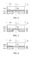
Referring to FIG. 2, a cross-sectional view of an exemplary embodiment of a decorative structure along the line 2-2′ in FIG. 1 and the fabrication method thereof are illustrated. The decorative structure 20 comprises a transparent substrate 100, and a low diffusivity material layer 202 and a protective layer 208 thereon. First, the transparent substrate 100, such as glass, is provided. The transparent substrate 100 has a touch surface (i.e. sensing surface) 100 c and a non-sensing surface 100 d opposite thereto. The non-sensing surface 100 d has an image display region 100 b and a non-image display area 100 a (as shown in FIG. 1).
Next, a low diffusivity material layer 202 is disposed on the non-sensing surface 100 d of the transparent substrate 100 and corresponds to the non-image display area 100 a to expose the image display area 100 b of the non-sensing surface 100 d. In particular, in the embodiment, the low diffusivity material layer 202 has a reflectivity of less than 10%. In one embodiment, the low diffusivity material layer 202 may comprise transparent ink which may be formed on the transparent substrate 100 by coating or other suitable methods. The low diffusivity material layer 202 may have a thickness in a range of 2 μm to 3 μm.
In another embodiment, the low diffusivity material layer 202 may comprise poly(ethylene terephthalate) (PET) or triacetyl cellulose (TAC), and be formed on the transparent substrate 100 by deposition or other suitable methods. The low diffusivity material layer 202 may have a thickness greater than or equal to 100 μm.
Next, a protective layer 208 is disposed on the low diffusivity material layer 202 and has at least an opening pattern 208 a to serve as a virtual function key region. It is noted that the opening pattern 208 a may be any pattern and is not limited to the pattern shown in FIG. 1, and is based on the design demands. Further, a backlight (not shown) is typically disposed underlying the opening pattern 208 a to allow a light L to sequentially pass through the low diffusivity material layer 202 and the transparent substrate 100 from the opening pattern 208 a. In one embodiment, the protective layer 208 may comprise printing ink and be formed on the low diffusivity material layer 202 by printing, coating or other suitable methods. The protective layer 208 may have a thickness in a range of 5 μm to 50 μm.
In the embodiment, the decorative structure 20 further comprises decorative layers 204 and 206 disposed between the low diffusivity material layer 202 and the protective layer 208. For example, the decorative layer 204 having at least an opening pattern 204 a corresponding to the opening pattern 208 a is formed between the low diffusivity material layer 202 and the protective layer 208 before forming the protective layer 208. The decorative layer 204 may have a specific color to determine the color of the decorative region (i.e. the non-image display area 100 a). In one embodiment, the decorative layer 204 may comprise printing ink and be formed on the low diffusivity material layer 202 by printing, coating or other suitable methods. The decorative layer 204 may have a thickness in a range of 5 μm to 50 μm.
Next, a decorative layer 206 is formed between the decorative layer 204 and the protective layer 208 and fills the opening pattern 204 a of the decorative layer 204. The decorative layer 206 may have a specific color or be colorless to determine the color of the virtual function keys. In the embodiment, the materials and the fabrication methods of the decorative layer 206 may be the same as or similar to that of the decorative layer 204.
According to the foregoing embodiment, since the light L passing through the opening patterns 208 a and 204 a needs to pass through the transparent substrate 100 from the low diffusivity material layer 202, the effect of light diffusion is reduced by the low diffusivity material layer 202, thereby preventing the halo effect from occurring near the regions of the opening patterns 208 a and 204 a. Therefore, the identification of the virtual function keys for users is maintained or improved.
Referring to FIG. 3, a cross-sectional view of another exemplary embodiment of a decorative structure along the line 2-2′ in FIG. 1 and the fabrication method thereof are illustrated. Elements in FIG. 3 that are the same as those in FIG. 2 are labeled with the same reference numbers as in FIG. 2 and are not described again for brevity. In the embodiment, the decorative structure 20 has a structure similar to that of the decorative structure shown in FIG. 2. Unlike the embodiment shown in FIG. 2, the decorative layer 204 having the opening pattern 204 a is disposed between the transparent substrate 100 and the low diffusivity material layer 202. That is, the decorative layer 204 having at least one opening pattern 204 a corresponding to the opening pattern 208 a may be formed on the glass substrate 100 before forming the low diffusivity material layer 202. In the embodiment, the low diffusivity material layer 202 can be a decorative layer having a specific color or being colorless to determine the color of the virtual function keys. Therefore, the decorative layer 206 does not need to be formed (as shown in FIG. 2). Compared to the embodiment of FIG. 2, the process is further simplified.
According to the foregoing embodiment, since the light L passing through the opening patterns 208 a and 204 a need to pass through the transparent substrate 100 from the low diffusivity material layer 202, the halo effect is prevented from occurring in the regions near the opening patterns 208 a and 204 a due to the low diffusivity material layer 202. Therefore, the identification of the virtual function keys for users is maintained or improved.
Referring to FIG. 4, a cross-sectional view of another exemplary embodiment of a decorative structure along the line 2-2′ in FIG. 1 and the fabrication method thereof are illustrated. Elements in FIG. 4 that are the same as those in FIG. 2 are labeled with the same reference numbers as in FIG. 2 and are not described again for brevity. In the embodiment, the decorative structure 20 has a structure similar to that of the decorative structure shown in FIG. 2. Unlike the embodiment shown in FIG. 2, the low diffusivity material layer 202 has at least one opening pattern 202 a corresponding to the opening pattern 208 a, such that the decorative layer 206 is formed on the low diffusivity material layer 202 and fills the opening pattern 202 a. In the embodiment, the low diffusivity material layer 202 may have a specific color or be colorless to determine the color of the decorative region (i.e. the non-image display area 100 a). Therefore, the decorative layer 204 does not need to be formed (as shown in FIG. 2). Compared to the embodiment of FIG. 2, the process is further simplified.
According to the foregoing embodiment, the regions near the opening pattern 202 a are prevented from the halo effect by the low diffusivity material layer 202. Therefore, the identification of the virtual function keys for users is maintained or improved.
Referring to FIG. 5, a cross-sectional view of another exemplary embodiment of a decorative structure along the line 3-3′ in FIG. 1 and the fabrication method thereof are illustrated. Elements in FIG. 5 that are the same as those in FIG. 2 are labeled with the same reference numbers as in FIG. 2 and are not described again for brevity. In the embodiment, the protective layer 208 of the decorative structure 20 has at least one opening pattern 208 b to serve as a charging indicator region. It is noted that the opening pattern 208 b can be any pattern and is not limited to the pattern shown in FIG. 1, and is based on the design demands. Further, a backlight (not shown) is typically disposed underlying the opening pattern 208 b to allow a light L′ to sequentially pass through the low diffusivity material layer 202 and the transparent substrate 100 from the opening pattern 208 b. In one embodiment, the materials and the fabrication methods of the protective layer 208 may be the same as or similar to the decorative layer 204 (as shown in FIG. 2) and be a specific color to determine the color of the decorative region (i.e. the non-image display area 100 a). In another embodiment, a decorative layer (not shown) is formed between the low diffusivity material layer 202 and the protective layer 208 to determine the color of the decorative region.
According to the foregoing embodiment, since the light L′ passing through the opening pattern 208 a needs to pass through the transparent substrate 100 from the low diffusivity material layer 202, the halo effect is prevented from occurring in the regions near the opening pattern 208 b due to the low diffusivity material layer 202. Therefore, the identification of the charging indicator region for users is maintained or improved.
Referring to FIG. 6, a cross-sectional view of another exemplary embodiment of a decorative structure along the line 3-3′ in FIG. 1 and the fabrication method thereof are illustrated. Elements in FIG. 6 that are the same as those in FIG. 5 are labeled with the same reference numbers as in FIG. 5 and are not described again for brevity. In the embodiment, the decorative structure 20 has a structure similar to that of the decorative structure shown in FIG. 5. Unlike the embodiment shown in FIG. 5, the low diffusivity material layer 202 has at least one opening pattern 202 b corresponding to the opening pattern 208 a. In the embodiment, the low diffusivity material layer 202 may have a specific color or be colorless to determine the color of the decorative region (i.e. the non-image display area 100 a). In one embodiment, the materials and the fabrication methods of the protective layer 208 may be the same as or similar to the decorative layer 204 (as shown in FIG. 2) and be a specific color to determine the color of the decorative region (i.e. the non-image display area 100 a). In another embodiment, a decorative layer (not shown) is formed between the low diffusivity material layer 202 and the protective layer 208 to determine the color of the decorative region.
According to the foregoing embodiment, the halo effect is prevented from occurring in the regions near the opening pattern 202 b due to the low diffusivity material layer 202. Therefore, the identification of the charging indicator region for users is maintained or improved.
While the invention has been described by way of example and in terms of preferred embodiment, it is to be understood that the invention is not limited thereto. To the contrary, it is intended to cover various modifications and similar arrangements (as would be apparent to those skilled in the art). Therefore, the scope of the appended claims should be accorded the broadest interpretation so as to encompass all such modifications and similar arrangements.

Claims (36)

What is claimed is:
1. A decorative structure for a touch sensing device, comprising:
a transparent substrate, having a non-touch surface which has a non-image display area;
a low diffusivity material layer, disposed on the non-touch surface of the transparent substrate and corresponding to the non-image display area to expose a portion of the non-touch surface outside of the non-image display area, wherein the low diffusivity material layer has a reflectivity of less than 10%; and
a protective layer, disposed on the low diffusivity material layer and having at least a first opening pattern to allow a light to sequentially pass through the low diffusivity material layer and the transparent substrate from the first opening pattern.
2. The decorative structure of claim 1, further comprising:
a first decorative layer, disposed between the low diffusivity layer and the protective layer, and having at least a second opening pattern corresponding to the first opening pattern; and
a second decorative layer, disposed between the first decorative layer and the protective layer, and filling the second opening pattern of the first decorative layer.
3. The decorative structure of claim 1, further comprising a first decorative layer, disposed between the transparent substrate and the low diffusivity material layer, wherein the first decorative layer has at least a second opening pattern corresponding to the first opening pattern, such that the low diffusivity material layer fills the second opening pattern of the first decorative layer to serve as a second decorative layer.
4. The decorative structure of claim 1, wherein the low diffusivity material layer has at least a second opening pattern corresponding to the first opening pattern to serve as a first decorative layer, and the decorative structure further comprises a second decorative layer disposed between the low diffusivity material layer and the protective layer and filling the second opening pattern of the low diffusivity material layer.
5. The decorative structure of claim 1, wherein the low diffusivity material layer comprises transparent ink.
6. The decorative structure of claim 5, wherein the low diffusivity material layer has a thickness in a range of 2 μm to 3 μm.
7. The decorative structure of claim 1, wherein the low diffusivity material layer comprises poly(ethylene terephthalate) (PET) or triacetyl cellulose (TAC).
8. The decorative structure of claim 7, wherein the low diffusivity material layer has a thickness greater than or equal to 100 μm.
9. The decorative structure of claim 1, wherein the low diffusivity material layer has at least a second opening pattern corresponding to the first opening pattern.
10. A method for fabricating a decorative structure for a touch sensing device, comprising:
providing a transparent substrate having a non-touch surface which has a non-image display area;
forming a low diffusivity material layer on the non-touch surface corresponding to the non-image display area to expose a portion of the non-touch surface outside of the non-image display area, wherein the low diffusivity material layer has a reflectivity of less than 10%; and
forming a protective layer on the low diffusivity material layer, wherein the low diffusivity material layer has at least a first opening pattern to allow a light to sequentially pass through the low diffusivity material layer and the transparent substrate from the first opening pattern.
11. The method of claim 10, further comprising:
forming a first decorative layer between the low diffusivity layer and the protective layer, wherein the first decorative layer has at least a second opening pattern corresponding to the first opening pattern; and
forming a second decorative layer between the first decorative layer and the protective layer, and filling the second opening pattern of the first decorative layer.
12. The method of claim 10, further comprising forming a first decorative layer between the transparent substrate and the low diffusivity material layer, wherein the first decorative layer has at least a second opening pattern corresponding to the first opening pattern, such that the low diffusivity material layer fills the second opening pattern of the first decorative layer to serve as a second decorative layer.
13. The method of claim 10, further comprising:
forming at least a second opening pattern in the low diffusivity material layer to serve as a first decorative layer, wherein the second opening pattern corresponds to the first opening pattern; and
forming a second decorative layer between the low diffusivity material layer and the protective layer and filling the second opening pattern of the low diffusivity material layer.
14. The method of claim 10, wherein the low diffusivity material layer comprises transparent ink.
15. The method of claim 14, wherein the low diffusivity material layer has a thickness in a range of 2 μm to 3 μm.
16. The method of claim 10, wherein the low diffusivity material layer comprises poly(ethylene terephthalate) (PET) or triacetyl cellulose (TAC).
17. The method of claim 16, wherein the low diffusivity material layer has a thickness greater than or equal to 100 μm.
18. The method of claim 10, wherein the low diffusivity material layer has at least a second opening pattern corresponding to the first opening pattern.
19. A decorative structure for a touch sensing device, comprising:
a transparent substrate, having a non-touch surface which has a non-image display area;
a low diffusivity material layer, disposed on the non-touch surface of the transparent substrate and corresponding to the non-image display area, wherein the low diffusivity material layer has a reflectivity of less than 10%;
a protective layer, disposed on the low diffusivity material layer and having at least a first opening pattern to allow a light to sequentially pass through the low diffusivity material layer and the transparent substrate from the first opening pattern;
a first decorative layer, disposed between the low diffusivity layer and the protective layer, and having at least a second opening pattern corresponding to the first opening pattern; and
a second decorative layer, disposed between the first decorative layer and the protective layer, and filling the second opening pattern of the first decorative layer.
20. The decorative structure of claim 19, wherein the low diffusivity material layer comprises transparent ink.
21. The decorative structure of claim 20, wherein the low diffusivity material layer has a thickness in a range of 2 μm to 3 μm.
22. The decorative structure of claim 19, wherein the low diffusivity material layer comprises poly(ethylene terephthalate) (PET) or triacetyl cellulose (TAC).
23. The decorative structure of claim 22, wherein the low diffusivity material layer has a thickness greater than or equal to 100 μm.
24. The decorative structure of claim 19, wherein the low diffusivity material layer has at least a second opening pattern corresponding to the first opening pattern.
25. A decorative structure for a touch sensing device, comprising:
a transparent substrate, having a non-touch surface which has a non-image display area;
a low diffusivity material layer, disposed on the non-touch surface of the transparent substrate and corresponding to the non-image display area, wherein the low diffusivity material layer has a reflectivity of less than 10%;
a protective layer, disposed on the low diffusivity material layer and having at least a first opening pattern to allow a light to sequentially pass through the low diffusivity material layer and the transparent substrate from the first opening pattern; and
a first decorative layer, disposed between the transparent substrate and the low diffusivity material layer, wherein the first decorative layer has at least a second opening pattern corresponding to the first opening pattern, such that the low diffusivity material layer fills the second opening pattern of the first decorative layer to serve as a second decorative layer.
26. The decorative structure of claim 25, wherein the low diffusivity material layer comprises transparent ink.
27. The decorative structure of claim 26, wherein the low diffusivity material layer has a thickness in a range of 2 μm to 3 μm.
28. The decorative structure of claim 25, wherein the low diffusivity material layer comprises poly(ethylene terephthalate) (PET) or triacetyl cellulose (TAC).
29. The decorative structure of claim 28, wherein the low diffusivity material layer has a thickness greater than or equal to 100 μm.
30. The decorative structure of claim 25, wherein the low diffusivity material layer has at least a second opening pattern corresponding to the first opening pattern.
31. A decorative structure for a touch sensing device, comprising:
a transparent substrate, having a non-touch surface which has a non-image display area;
a low diffusivity material layer, disposed on the non-touch surface of the transparent substrate and corresponding to the non-image display area, wherein the low diffusivity material layer has a reflectivity of less than 10%;
a protective layer, disposed on the low diffusivity material layer and having at least a first opening pattern to allow a light to sequentially pass through the low diffusivity material layer and the transparent substrate from the first opening pattern, wherein the low diffusivity material layer has at least a second opening pattern corresponding to the first opening pattern to serve as a first decorative layer; and
a second decorative layer, disposed between the low diffusivity material layer and the protective layer and filling the second opening pattern of the low diffusivity material layer.
32. The decorative structure of claim 31, wherein the low diffusivity material layer comprises transparent ink.
33. The decorative structure of claim 32, wherein the low diffusivity material layer has a thickness in a range of 2 μm to 3 μm.
34. The decorative structure of claim 31, wherein the low diffusivity material layer comprises poly(ethylene terephthalate) (PET) or triacetyl cellulose (TAC).
35. The decorative structure of claim 34, wherein the low diffusivity material layer has a thickness greater than or equal to 100 μm.
36. The decorative structure of claim 31, wherein the low diffusivity material layer has at least a second opening pattern corresponding to the first opening pattern.
US13/572,365 2012-08-10 2012-08-10 Decorative structure for touch sensing device and fabrication method thereof Active 2033-01-02 US8884902B2 (en)

Priority Applications (3)

Application Number Priority Date Filing Date Title
US13/572,365 US8884902B2 (en) 2012-08-10 2012-08-10 Decorative structure for touch sensing device and fabrication method thereof
TW101135042A TWI472839B (en) 2012-08-10 2012-09-25 Decorative structure for touch sensing device and fabrication method thereof
CN201210367805.0A CN103576970B (en) 2012-08-10 2012-09-28 Decorative structure for touch sensing device and fabrication method thereof

Applications Claiming Priority (1)

Application Number Priority Date Filing Date Title
US13/572,365 US8884902B2 (en) 2012-08-10 2012-08-10 Decorative structure for touch sensing device and fabrication method thereof

Publications (2)

Publication Number Publication Date
US20140043246A1 US20140043246A1 (en) 2014-02-13
US8884902B2 true US8884902B2 (en) 2014-11-11

Family

ID=50048897

Family Applications (1)

Application Number Title Priority Date Filing Date
US13/572,365 Active 2033-01-02 US8884902B2 (en) 2012-08-10 2012-08-10 Decorative structure for touch sensing device and fabrication method thereof

Country Status (3)

Country Link
US (1) US8884902B2 (en)
CN (1) CN103576970B (en)
TW (1) TWI472839B (en)

Families Citing this family (5)

* Cited by examiner, † Cited by third party
Publication number Priority date Publication date Assignee Title
US20130279089A1 (en) * 2012-01-05 2013-10-24 Htc Corporation Cover, electronic device and manufacturing method for cover
KR101970526B1 (en) * 2012-04-26 2019-04-19 엘지전자 주식회사 Mobile terminal
CN104123022B (en) * 2013-04-24 2017-07-28 宸鸿科技(厦门)有限公司 Contact panel and its covering plate structure
TW201510802A (en) * 2013-09-14 2015-03-16 Wintek Corp Touch panel
CN105573532B (en) * 2014-10-09 2019-09-03 宸鸿科技(厦门)有限公司 Touch panel structure provided and its manufacturing method

Citations (7)

* Cited by examiner, † Cited by third party
Publication number Priority date Publication date Assignee Title
US4771277A (en) * 1986-05-02 1988-09-13 Barbee Peter F Modular touch sensitive data input device
US20040263670A1 (en) * 2003-06-18 2004-12-30 Ryo Yamasaki Display device with image sensing device
US20090195739A1 (en) * 2008-02-04 2009-08-06 Himax Display, Inc. Liquid crystal on silicon display panel and electronic device using the same
US7598926B2 (en) * 2004-02-17 2009-10-06 Panasonic Corporation Display panel, control display panel and method for integrally molding insert material
US20100182740A1 (en) * 2009-01-21 2010-07-22 Mitsubishi Electric Corporation Display and input device and method for manufacturing the same
US20110128114A1 (en) * 2009-06-30 2011-06-02 Sony Corporation Touch panel and method of manufacturing the same
US8203659B2 (en) * 2010-08-13 2012-06-19 Litemax Electronics Inc. LCD display and gaming machine combination

Family Cites Families (2)

* Cited by examiner, † Cited by third party
Publication number Priority date Publication date Assignee Title
TWM356139U (en) * 2008-12-30 2009-05-01 Mildex Optical Inc Touch panel with light adjustment function
CN202189343U (en) * 2011-08-08 2012-04-11 东莞联胜液晶显示器有限公司 Touch control panel and the touch control display device

Patent Citations (7)

* Cited by examiner, † Cited by third party
Publication number Priority date Publication date Assignee Title
US4771277A (en) * 1986-05-02 1988-09-13 Barbee Peter F Modular touch sensitive data input device
US20040263670A1 (en) * 2003-06-18 2004-12-30 Ryo Yamasaki Display device with image sensing device
US7598926B2 (en) * 2004-02-17 2009-10-06 Panasonic Corporation Display panel, control display panel and method for integrally molding insert material
US20090195739A1 (en) * 2008-02-04 2009-08-06 Himax Display, Inc. Liquid crystal on silicon display panel and electronic device using the same
US20100182740A1 (en) * 2009-01-21 2010-07-22 Mitsubishi Electric Corporation Display and input device and method for manufacturing the same
US20110128114A1 (en) * 2009-06-30 2011-06-02 Sony Corporation Touch panel and method of manufacturing the same
US8203659B2 (en) * 2010-08-13 2012-06-19 Litemax Electronics Inc. LCD display and gaming machine combination

Also Published As

Publication number Publication date
TWI472839B (en) 2015-02-11
CN103576970B (en) 2017-04-12
US20140043246A1 (en) 2014-02-13
TW201407230A (en) 2014-02-16
CN103576970A (en) 2014-02-12

Similar Documents

Publication Publication Date Title
US8581880B2 (en) Capacitive touch display panel
US8994680B2 (en) Systems for displaying images
US8884902B2 (en) Decorative structure for touch sensing device and fabrication method thereof
US20140340364A1 (en) Touch display panel
US9872400B2 (en) Touch panel and method for manufacturing the same
US9874967B2 (en) Touch-panel display device
US10133378B2 (en) Touch device
CN105324705B (en) With the display of blue pigment layer under black matrix"
US10817093B2 (en) Touch display panel and manufacturing method thereof
US9226394B2 (en) Touch-sensing substrate, display panel, and patterned light-shielding layer
JP5927915B2 (en) Touch panel sensor substrate and method for manufacturing the substrate
KR20150095449A (en) Touch sensor and method for manufacturing the touch sensor
US20140062959A1 (en) Touch panel
KR20140030727A (en) Touch panel and method for manufacturing the same
CN103294291A (en) Touch control board
US10203832B2 (en) Color film substrate, manufacturing method thereof and display device
CN103092379B (en) The manufacture method of image display system and touch sensing device
US10042452B2 (en) Touch sensor device and method for forming the same
US9274638B2 (en) Touch panel
US20160041658A1 (en) Display device
US20130043081A1 (en) Multi-function touch panel
US9285513B2 (en) Display apparatus with symmetric diffusion film
US20150049259A1 (en) Touch sensor module and manufacturing method thereof
US10274653B2 (en) Display device
US9323365B2 (en) Masking an outer perimeter of a touch screen

Legal Events

Date Code Title Description
AS Assignment

Owner name: HTC CORPORATION, TAIWAN

Free format text: ASSIGNMENT OF ASSIGNORS INTEREST;ASSIGNORS:HSUEH, FU-YUAN;HUANG, YUNG-MING;REEL/FRAME:029115/0141

Effective date: 20120912

STCF Information on status: patent grant

Free format text: PATENTED CASE

MAFP Maintenance fee payment

Free format text: PAYMENT OF MAINTENANCE FEE, 4TH YEAR, LARGE ENTITY (ORIGINAL EVENT CODE: M1551)

Year of fee payment: 4

MAFP Maintenance fee payment

Free format text: PAYMENT OF MAINTENANCE FEE, 8TH YEAR, LARGE ENTITY (ORIGINAL EVENT CODE: M1552); ENTITY STATUS OF PATENT OWNER: LARGE ENTITY

Year of fee payment: 8