US8884358B2 - Method of making a non-volatile memory (NVM) cell structure - Google Patents
Method of making a non-volatile memory (NVM) cell structure Download PDFInfo
- Publication number
- US8884358B2 US8884358B2 US13/748,808 US201313748808A US8884358B2 US 8884358 B2 US8884358 B2 US 8884358B2 US 201313748808 A US201313748808 A US 201313748808A US 8884358 B2 US8884358 B2 US 8884358B2
- Authority
- US
- United States
- Prior art keywords
- charge storage
- oxide
- layer
- storage elements
- insulating material
- Prior art date
- Legal status (The legal status is an assumption and is not a legal conclusion. Google has not performed a legal analysis and makes no representation as to the accuracy of the status listed.)
- Active
Links
Images


Classifications
-
- H—ELECTRICITY
- H10—SEMICONDUCTOR DEVICES; ELECTRIC SOLID-STATE DEVICES NOT OTHERWISE PROVIDED FOR
- H10B—ELECTRONIC MEMORY DEVICES
- H10B43/00—EEPROM devices comprising charge-trapping gate insulators
-
- H01L29/401—
-
- H—ELECTRICITY
- H10—SEMICONDUCTOR DEVICES; ELECTRIC SOLID-STATE DEVICES NOT OTHERWISE PROVIDED FOR
- H10D—INORGANIC ELECTRIC SEMICONDUCTOR DEVICES
- H10D64/00—Electrodes of devices having potential barriers
- H10D64/01—Manufacture or treatment
- H10D64/031—Manufacture or treatment of data-storage electrodes
- H10D64/037—Manufacture or treatment of data-storage electrodes comprising charge-trapping insulators
-
- B—PERFORMING OPERATIONS; TRANSPORTING
- B82—NANOTECHNOLOGY
- B82Y—SPECIFIC USES OR APPLICATIONS OF NANOSTRUCTURES; MEASUREMENT OR ANALYSIS OF NANOSTRUCTURES; MANUFACTURE OR TREATMENT OF NANOSTRUCTURES
- B82Y10/00—Nanotechnology for information processing, storage or transmission, e.g. quantum computing or single electron logic
-
- H01L29/4234—
-
- H—ELECTRICITY
- H10—SEMICONDUCTOR DEVICES; ELECTRIC SOLID-STATE DEVICES NOT OTHERWISE PROVIDED FOR
- H10D—INORGANIC ELECTRIC SEMICONDUCTOR DEVICES
- H10D30/00—Field-effect transistors [FET]
- H10D30/60—Insulated-gate field-effect transistors [IGFET]
- H10D30/68—Floating-gate IGFETs
- H10D30/6891—Floating-gate IGFETs characterised by the shapes, relative sizes or dispositions of the floating gate electrode
- H10D30/6893—Floating-gate IGFETs characterised by the shapes, relative sizes or dispositions of the floating gate electrode wherein the floating gate has multiple non-connected parts, e.g. multi-particle floating gate
-
- H—ELECTRICITY
- H10—SEMICONDUCTOR DEVICES; ELECTRIC SOLID-STATE DEVICES NOT OTHERWISE PROVIDED FOR
- H10D—INORGANIC ELECTRIC SEMICONDUCTOR DEVICES
- H10D30/00—Field-effect transistors [FET]
- H10D30/60—Insulated-gate field-effect transistors [IGFET]
- H10D30/69—IGFETs having charge trapping gate insulators, e.g. MNOS transistors
- H10D30/694—IGFETs having charge trapping gate insulators, e.g. MNOS transistors characterised by the shapes, relative sizes or dispositions of the gate electrodes
-
- H—ELECTRICITY
- H10—SEMICONDUCTOR DEVICES; ELECTRIC SOLID-STATE DEVICES NOT OTHERWISE PROVIDED FOR
- H10D—INORGANIC ELECTRIC SEMICONDUCTOR DEVICES
- H10D62/00—Semiconductor bodies, or regions thereof, of devices having potential barriers
- H10D62/10—Shapes, relative sizes or dispositions of the regions of the semiconductor bodies; Shapes of the semiconductor bodies
- H10D62/117—Shapes of semiconductor bodies
- H10D62/118—Nanostructure semiconductor bodies
-
- H—ELECTRICITY
- H10—SEMICONDUCTOR DEVICES; ELECTRIC SOLID-STATE DEVICES NOT OTHERWISE PROVIDED FOR
- H10D—INORGANIC ELECTRIC SEMICONDUCTOR DEVICES
- H10D62/00—Semiconductor bodies, or regions thereof, of devices having potential barriers
- H10D62/80—Semiconductor bodies, or regions thereof, of devices having potential barriers characterised by the materials
- H10D62/81—Semiconductor bodies, or regions thereof, of devices having potential barriers characterised by the materials of structures exhibiting quantum-confinement effects, e.g. single quantum wells; of structures having periodic or quasi-periodic potential variation
- H10D62/812—Single quantum well structures
- H10D62/814—Quantum box structures
-
- H—ELECTRICITY
- H10—SEMICONDUCTOR DEVICES; ELECTRIC SOLID-STATE DEVICES NOT OTHERWISE PROVIDED FOR
- H10D—INORGANIC ELECTRIC SEMICONDUCTOR DEVICES
- H10D64/00—Electrodes of devices having potential barriers
- H10D64/01—Manufacture or treatment
- H10D64/031—Manufacture or treatment of data-storage electrodes
- H10D64/035—Manufacture or treatment of data-storage electrodes comprising conductor-insulator-conductor-insulator-semiconductor structures
Definitions
- This disclosure relates generally to semiconductor manufacturing, and more specifically, to the making of NVM cells.
- Non-volatile memories which are a major portion of the semiconductor industry, are often found on integrated circuits that have one or more processing units.
- NVM cells One of the characteristics of NVM cells is that writing cells includes both erasing and programming. Both of these operations typically require higher voltages, commonly significantly higher, than are required for general purpose circuits such as the logic transistors used for providing a processing unit. Also, both programming and erasing require significantly more time than reading. Thus, there is the continuing effort to reduce the voltages required for programming and erase and reduce the time for performing those functions.
- erasing which is typically removing electrons from a storage layer.
- nanocrystals being used for the storage layer, this is achieved using tunneling and that is most commonly done using top erase in which electrons tunnel from the nanocrystals to the overlying control gate.
- FIG. 1 is a cross section of an NVM cell structure at a stage in processing according to a first embodiment
- FIG. 2 is a cross section of the NVM cell structure of FIG. 1 at a subsequent stage in processing
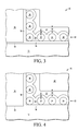
- FIG. 3 is a cross section of the NVM cell structure of FIG. 2 at a subsequent stage in processing
- FIG. 4 is a cross section of the NVM cell structure of FIG. 3 at a subsequent stage in processing
- FIG. 5 is a cross section of the NVM cell structure of FIG. 4 at a subsequent stage in processing
- FIG. 6 is a cross section of an NVM cell structure at a stage in processing according to a second embodiment
- FIG. 7 is a cross section of the NVM cell structure of FIG. 6 at a subsequent stage in processing
- FIG. 8 is a cross section of an NVM cell structure at a stage in processing according to a third embodiment
- FIG. 9 is a cross section of the NVM cell structure of FIG. 8 at a subsequent stage in processing
- FIG. 10 is a cross section of the NVM cell structure of FIG. 9 at a subsequent stage in processing
- FIG. 11 is a cross section of an NVM cell structure at a stage in processing according to a fourth embodiment
- FIG. 12 is a cross section of the NVM cell structure of FIG. 11 at a subsequent stage in processing.
- FIG. 13 is a cross section of a pair of NVM cell structures useful in understanding the embodiments.
- a dielectric between a storage layer of nanocyrstals has an interface between the dielectric and a control gate that is substantially planar instead of conformal to the underlying nanocrystals which is the normal condition absent special conditioning to arrive at the planar condition.
- the thickness of the dielectric is relatively thin directly over the nanocrystals. The result is reduced capacitance between the control gate and the nanocrystals for a given dielectric thickness directly over the nanocrystals.
- the region directly over the nanocrystals is relatively thin for ease of tunneling but the capacitance is minimized for this thickness by avoiding having the control gate conformal with the nanocrystals. This is better understood by reference to the specification and the drawings.
- the semiconductor substrate described herein can be any semiconductor material or combinations of materials, such as gallium arsenide, silicon germanium, silicon-on-insulator (SOI), silicon, monocrystalline silicon, the like, and combinations of the above.
- SOI silicon-on-insulator
- NVM non-volatile memory
- FIG. 1 Shown in FIG. 1 is a non-volatile memory (NVM) cell structure 10 having a substrate 12 , a dielectric layer 18 over substrate 12 , a select gate 14 over dielectric layer 18 , a dielectric layer 16 over substrate 12 in an area adjacent to dielectric layer 18 and along a sidewall of select gate 14 , nanocrystals 20 , 22 , 24 , and 26 laterally over dielectric layer 16 where dielectric layer 16 is over substrate 12 , and nanocrystals 28 and 30 on dielectric layer 16 along the sidewall of select gate 14 .
- Nanocrystals 20 , 22 , 24 , 26 , 28 , and 30 comprise a plurality of nanocrystals 32 .
- Dielectric layer 18 may be thermal oxide that is grown at high temperature.
- Dielectric layer 16 may be a thermal oxide that causes oxide growth on the sidewall of select gate 14 and may be thicker on the sidewall due to the select gate in the case of select gate 14 being polysilicon.
- Dielectric layer 18 may be about 30 Angstroms in thickness.
- Dielectric layer 16 may be about 60 Angstroms in thickness.
- Nanocrystals 32 may each have a diameter of about 120 Angstroms.
- NVM cell structure 10 of FIG. 1 is a structure from which multiple embodiments may be developed.
- Dielectric layer 34 may be a conformal high temperature oxide.
- Dielectric layer 34 has a thickness 36 above nanocrystals 32 . Particularly shown is nanocrystal 22 as a example of thickness 36 being directly over a nanocrystal. Thickness 36 may be about 40 Angstroms.
- High temperature oxide can have parameters adjusted to obtain conformality or planar behavior and various degrees between those two behaviors. For more planar, higher temperature and higher pressure are used, and a higher concentration of disilane is used. The quality of the oxide is better for conformal high temperature oxide.
- NVM cell structure 10 after depositing a dielectric layer 37 that is planar meaning that it is tends to fill in the gaps with a resulting surface that is much more planar than would occur by forming a layer that is conformal.
- Dielectric layer 37 may be high temperature oxide in which the parameters are selected so that its behavior is planar.
- Dielectric layer 37 has a thickness directly above the nanocrystals of about 40 Angstroms. The example of this is shown with nanocrystal 24 in which a thickness 38 of dielectric layer 37 is shown directly above nanocrystal 24 . Thickness 38 may be about 40 Angstroms.
- Dielectric layer 37 is substantially planar in the horizontal direction of nanocrystals 20 , 22 , 24 , and 26 . Dielectric layer 37 would be thinner vertically along nanocrystals 28 and 30 than horizontally over nanocrystals 20 , 22 , 24 , and 26 .
- NVM cell structure 10 after forming a control gate 40 over dielectric layer 37 .
- the horizontally aligned nanocrystals are the ones that will have electrons present as a result of being programmed.
- Nanocrystals 28 and 30 are essentially irrelevant in terms of passing charge for programming and erasing.
- the distance from each of the horizontal nanocrystals to control gate 40 is thickness 36 plus distance 38 which is 40 Angstroms plus 40 Angstroms which equals 80 Angstroms.
- FIG. 5 Shown in FIG. 5 is an NVM cell structure 50 after a dielectric 52 has been deposited on the NVM cell structure 10 of FIG. 1 .
- Dielectric 52 is a high temperature oxide that is deposited using substantially conformal parameter settings but due to the thickness, is substantially planar.
- the distance to the top surface of dielectric layer 52 from the top of a horizontal nanocrystal is a thickness 54 which may be about 200 Angstroms.
- the example is this case of FIG. 5 is from the top of nanocrystal 24 to the top surface of dielectric layer 52 of FIG. 5 .
- NVM cell structure 50 after an etch back which reduces the thickness of dielectric layer 52 to have a top surface over the horizontal nanocrystals to a thickness 56 which may be 80 Angstroms.
- This etch back may be isotropic.
- the etchback itself tends to increase the planarity of the top surface of dielectric layer 52 .
- NVM cell structure 50 after forming a control gate 58 over dielectric layer 52 so that the horizontal nanocrystals are, at the closest point, a thickness 56 from control gate 58 .
- Control gate 58 in areas between the horizontal nanocrystals, is a further distance from the nanocrystals than thickness 56 .
- the contribution to the capacitance between control gate 58 and the nanocrystals is lessened by the top surface of dielectric 52 being substantially planar.
- FIG. 8 Shown in FIG. 8 is an NVM cell structure 60 after growing a thin oxide layer 62 on nanocrystals 32 .
- Oxide layer 62 is shown, by way of example, on nanocrystal 22 .
- Oxide layer 62 may be about 20 Angstrom thick.
- Layer 62 is particularly convenient to be grown oxide because of the control in terms of thickness and high quality of the resulting layer of such a process. It may be possible to provide a protective layer using a different material such as nitride. Oxide layer 62 may also adhere particularly well to a subsequently deposited hot temperature oxide layer.
- NVM cell structure 60 after depositing a planar layer of high temperature oxide having a thickness 66 directly over the horizontal nanocrystals such as nancrystal 22 .
- oxide layer 62 coating the nanocrystals, there is additional protection for the nanocrystals so that the likelihood the planar high temperature oxide deposition will be sufficient.
- Thickness 66 may be about 60 Angstroms so that the total of thickness 66 and the thickness of oxide layer 62 is about 80 Angstroms.
- control gate 68 Shown in FIG. 10 is NVM cell structure 60 after forming a control gate 68 over dielectric layer 68 . This shows that control gate 68 , at the closest points to the nanocrystals, is distance 66 from the nanocrystals but is further than that distance in the areas between nanocrystals.
- an NVM cell structure 70 having a substrate 72 , a dielectric layer 74 over substrate 72 , a plurality of nanocrystals 84 , and a dielectric layer 86 over dielectric layer 74 and around and above nanocrystals 84 .
- Nanocrystals 84 comprise nanocrystals 76 , 78 , 80 , and 82 .
- Dielectric layer 86 may be formed by a deposition of conformal high temperature oxide and may be 250 Angstroms thick.
- NVM cell structure 70 after performing chemical mechanical polishing (CMP) to reduce the thickness of dielectric layer 86 over nanocrystals 84 to a thickness 90 which may be about 80 Angstroms.
- CMP chemical mechanical polishing
- a control gate 88 formed over dielectric layer 86 . Similar to previously described NVM cell structures, the distance between nanocrystals to the control gate is further than from the area directly over the nanocrystals. This reduces capacitance between the control gate and the nanocrystals for a given minimum distance such as distance 90 where the nanocrystals are directly under control gate 88 .
- NVM cell structure 91 has a conformal dielectric over nanocrystals 94 and 96 , a dielectric 92 that is conformal, and a control gate 93 over dielectric 92 .
- Shown is a radius 98 from the center of nanocrystal 94 to control gate 93 . This radius is the sum of a distance 102 from the center of nanocrystal 94 to its surface and a distance 100 from the top surface of nanocrystal to control gate 93 .
- the radius is at least twice that of radius 98 as shown in FIG.
- NVM cell structure 110 having nanocrystals 114 and 116 on a dielectric layer 112 .
- the top surface of the dielectric layer is considered substantially planar. If the top surface is perfectly planar, which may appear to be the case in the case of using CMP, then the radius is considered infinite.
- an NVM memory cell can have a substantially planar surface which results in less capacitance between the nanocrystals and the control gate for a given minimum distance between the nanocrystals and the control gate.
- the reduced capacitance results in allowing for a more electron tunneling out of the nanocrystals to the control gate, top side tunneling, prior to the tunneling from the substrate to the nanocrystals becoming equal to the top side tunneling.
- the applied erase voltage to the control gate has a bottom side portion between the substrate and the nanocrystals and a top side portion between the nanocrystals and the control gate.
- the ratio of the voltage across the top side and bottom side portions is based on the capacitance ratio at these portions.
- the percentage of the applied erase voltage that is between the control gate and the nanocrystals is increased. This similarly means that the bottom side voltage is decreased.
- the increase in top side voltage means increased tunneling where it is desired between the control gate and the nanocrystals and the decrease in bottom side voltage means decreased tunneling where it is not desired between the substrate and the nanocrystals. This may be allow for the benefits of some combination of reduced erase voltage, reduced erase time, and a greater differential between the erased state and the programmed state.
- the non-volatile memory device having a substrate and a charge storage layer.
- the charge storage layer includes a bottom layer of oxide, a layer of discrete charge storage elements on the bottom layer of oxide, and a top layer of oxide on the discrete charge storage elements.
- the non-volatile memory device further includes a control gate on the top layer of oxide, wherein a surface of the top layer of oxide facing a surface of the control gate is substantially planar.
- the device may have a further characterization by which a radius of curvature of the top layer of oxide over a majority of the discrete charge storage elements is at least twice a sum of a radius of the discrete charge storage element and a thickness of the top layer of oxide.
- the device may further include a select gate, wherein a portion of: the bottom layer of oxide, the discrete charge storage elements, and the top layer of oxide, are between one side of the control gate and one side of the select gate.
- the device may further include a thin layer of oxide on an outer surface of the charge storage elements.
- the device may further include a thickness of the top layer of oxide over at least one of the charge storage elements is less than a diameter of the at least one charge storage element.
- the method includes forming a first electrically insulating material on a substrate.
- the method further includes forming discrete charge storage elements on the first electrically insulating material.
- the method further includes depositing a second electrically insulating material over the discrete charge storage elements, wherein a top surface of the second electrically insulating material is substantially planar.
- the method may further include forming a control gate over the second electrically insulating material.
- the method may further include forming a select gate over a third insulating material.
- the method may have a further characterization by which a radius of curvature of the second electrically insulating material over one of the discrete charge storage elements is at least twice a sum of a radius of the one discrete charge storage element and a thickness of the second electrically insulating material.
- the method may further include growing an oxide layer on the discrete charge storage elements before depositing the second electrically insulating material.
- the method may have a further characterization by which a thickness of the second electrically insulating material over at least one of the discrete charge storage elements is less than a diameter of the at least one discrete charge storage element.
- the method may further include chemically-mechanically polishing the second electrically insulating material to be substantially planar.
- the method may further include depositing a conformal layer of electrically insulating material on the discrete charge storage elements before depositing the second electrically insulating material.
- the method may further include etching the second electrically insulating material to be substantially planar.
- Disclosed also is a method that includes forming a first oxide layer on a substrate.
- the method further includes forming discrete charge storage elements on the first oxide layer.
- the method further includes forming a second oxide layer that is planar on the discrete charge storage elements having a thickness that is less than a diameter of the charge storage elements.
- the method may have a further characterization by which the diameter of the discrete charge storage elements is between 10 to 20 nanometers and the thickness of the second oxide layer over the charge storage elements is between 6 and 10 nanometers.
- the method may further include depositing a conformal oxide layer on the charge storage elements before depositing the second oxide layer.
- the method may further include chemically-mechanically polishing the second oxide layer.
- the method may have a further characterization by which a radius of curvature of the second oxide layer over the discrete charge storage elements is at least twice a sum of a radius of the discrete charge storage elements and a thickness of the second oxide layer.
- the method may further include etching the second oxide layer.
- Coupled is not intended to be limited to a direct coupling or a mechanical coupling.
Landscapes
- Engineering & Computer Science (AREA)
- Chemical & Material Sciences (AREA)
- Nanotechnology (AREA)
- Physics & Mathematics (AREA)
- Mathematical Physics (AREA)
- Theoretical Computer Science (AREA)
- Crystallography & Structural Chemistry (AREA)
- Semiconductor Memories (AREA)
- Non-Volatile Memory (AREA)
- Manufacturing & Machinery (AREA)
Abstract
Description
Claims (17)
Priority Applications (4)
| Application Number | Priority Date | Filing Date | Title |
|---|---|---|---|
| US13/748,808 US8884358B2 (en) | 2013-01-24 | 2013-01-24 | Method of making a non-volatile memory (NVM) cell structure |
| JP2014007388A JP2014143418A (en) | 2013-01-24 | 2014-01-20 | Method of making non-volatile memory (nvm) cell structure |
| KR1020140007274A KR20140095435A (en) | 2013-01-24 | 2014-01-21 | Method of making a non-volatile memory(nvm) cell structure |
| TW103102811A TWI619231B (en) | 2013-01-24 | 2014-01-24 | Method of making non-volatile memory (NVM) cell structure |
Applications Claiming Priority (1)
| Application Number | Priority Date | Filing Date | Title |
|---|---|---|---|
| US13/748,808 US8884358B2 (en) | 2013-01-24 | 2013-01-24 | Method of making a non-volatile memory (NVM) cell structure |
Publications (2)
| Publication Number | Publication Date |
|---|---|
| US20140203347A1 US20140203347A1 (en) | 2014-07-24 |
| US8884358B2 true US8884358B2 (en) | 2014-11-11 |
Family
ID=51207060
Family Applications (1)
| Application Number | Title | Priority Date | Filing Date |
|---|---|---|---|
| US13/748,808 Active US8884358B2 (en) | 2013-01-24 | 2013-01-24 | Method of making a non-volatile memory (NVM) cell structure |
Country Status (4)
| Country | Link |
|---|---|
| US (1) | US8884358B2 (en) |
| JP (1) | JP2014143418A (en) |
| KR (1) | KR20140095435A (en) |
| TW (1) | TWI619231B (en) |
Citations (10)
| Publication number | Priority date | Publication date | Assignee | Title |
|---|---|---|---|---|
| US20050142751A1 (en) * | 2003-12-31 | 2005-06-30 | Dongbuanam Semiconductor Inc. | Methods for fabricating nonvolatile memory device |
| US20060063333A1 (en) * | 2003-11-04 | 2006-03-23 | Hee-Seog Jeon | Method of manufacturing split gate type nonvolatile memory device |
| US20070218633A1 (en) * | 2006-03-15 | 2007-09-20 | Prinz Erwin J | Silicided nonvolatile memory and method of making same |
| US20080076221A1 (en) * | 2006-09-26 | 2008-03-27 | Kang Sung-Taeg | Split gate memory cell method |
| US7517747B2 (en) | 2006-09-08 | 2009-04-14 | Freescale Semiconductor, Inc. | Nanocrystal non-volatile memory cell and method therefor |
| US20090256191A1 (en) * | 2008-04-15 | 2009-10-15 | White Ted R | Split gate non-volatile memory cell with improved endurance and method therefor |
| US20090256186A1 (en) * | 2008-04-15 | 2009-10-15 | Kang Sung-Taeg | Split gate non-volatile memory cell |
| US20110233655A1 (en) * | 2010-03-26 | 2011-09-29 | Kabushiki Kaisha Toshiba | Semiconductor memory device and method for manufacturing the semiconductor memory device |
| US20120135596A1 (en) * | 2008-01-30 | 2012-05-31 | Kang Sung-Taeg | Method of removing nanocrystals |
| US20120292683A1 (en) * | 2011-05-19 | 2012-11-22 | Loiko Konstantin V | Memory with discrete storage elements |
Family Cites Families (6)
| Publication number | Priority date | Publication date | Assignee | Title |
|---|---|---|---|---|
| JPH11186421A (en) * | 1997-12-25 | 1999-07-09 | Sony Corp | Nonvolatile semiconductor memory device and write / erase method therefor |
| TW546840B (en) * | 2001-07-27 | 2003-08-11 | Hitachi Ltd | Non-volatile semiconductor memory device |
| JP4786855B2 (en) * | 2002-05-22 | 2011-10-05 | シャープ株式会社 | Memory film structure, memory element, semiconductor device and electronic device |
| JP2004048062A (en) * | 2003-09-29 | 2004-02-12 | Sharp Corp | Manufacturing method of semiconductor nanocrystal and semiconductor memory device using the semiconductor nanocrystal |
| JP2010080827A (en) * | 2008-09-29 | 2010-04-08 | Toshiba Corp | Nonvolatile semiconductor memory, and method of manufacturing the same |
| US7985649B1 (en) * | 2010-01-07 | 2011-07-26 | Freescale Semiconductor, Inc. | Method of making a semiconductor structure useful in making a split gate non-volatile memory cell |
-
2013
- 2013-01-24 US US13/748,808 patent/US8884358B2/en active Active
-
2014
- 2014-01-20 JP JP2014007388A patent/JP2014143418A/en active Pending
- 2014-01-21 KR KR1020140007274A patent/KR20140095435A/en not_active Ceased
- 2014-01-24 TW TW103102811A patent/TWI619231B/en not_active IP Right Cessation
Patent Citations (11)
| Publication number | Priority date | Publication date | Assignee | Title |
|---|---|---|---|---|
| US20060063333A1 (en) * | 2003-11-04 | 2006-03-23 | Hee-Seog Jeon | Method of manufacturing split gate type nonvolatile memory device |
| US20050142751A1 (en) * | 2003-12-31 | 2005-06-30 | Dongbuanam Semiconductor Inc. | Methods for fabricating nonvolatile memory device |
| US20070218633A1 (en) * | 2006-03-15 | 2007-09-20 | Prinz Erwin J | Silicided nonvolatile memory and method of making same |
| US7517747B2 (en) | 2006-09-08 | 2009-04-14 | Freescale Semiconductor, Inc. | Nanocrystal non-volatile memory cell and method therefor |
| US20090166712A1 (en) * | 2006-09-08 | 2009-07-02 | Freescale Semiconductor, Inc. | Nanocrystal non-volatile memory cell and method therefor |
| US20080076221A1 (en) * | 2006-09-26 | 2008-03-27 | Kang Sung-Taeg | Split gate memory cell method |
| US20120135596A1 (en) * | 2008-01-30 | 2012-05-31 | Kang Sung-Taeg | Method of removing nanocrystals |
| US20090256191A1 (en) * | 2008-04-15 | 2009-10-15 | White Ted R | Split gate non-volatile memory cell with improved endurance and method therefor |
| US20090256186A1 (en) * | 2008-04-15 | 2009-10-15 | Kang Sung-Taeg | Split gate non-volatile memory cell |
| US20110233655A1 (en) * | 2010-03-26 | 2011-09-29 | Kabushiki Kaisha Toshiba | Semiconductor memory device and method for manufacturing the semiconductor memory device |
| US20120292683A1 (en) * | 2011-05-19 | 2012-11-22 | Loiko Konstantin V | Memory with discrete storage elements |
Also Published As
| Publication number | Publication date |
|---|---|
| TWI619231B (en) | 2018-03-21 |
| KR20140095435A (en) | 2014-08-01 |
| US20140203347A1 (en) | 2014-07-24 |
| JP2014143418A (en) | 2014-08-07 |
| TW201444029A (en) | 2014-11-16 |
Similar Documents
| Publication | Publication Date | Title |
|---|---|---|
| CN110880515B (en) | Semiconductor devices, electronic systems, and related methods | |
| US9165652B2 (en) | Split-gate memory cells having select-gate sidewall metal silicide regions and related manufacturing methods | |
| US8687426B2 (en) | Multi-semiconductor material vertical memory strings, strings of memory cells having individually biasable channel regions, memory arrays incorporating such strings, and methods of accesssing and forming the same | |
| JP5149539B2 (en) | Semiconductor device | |
| US9614048B2 (en) | Split gate flash memory structure and method of making the split gate flash memory structure | |
| US7800164B2 (en) | Nanocrystal non-volatile memory cell and method therefor | |
| US7804152B2 (en) | Recessed shallow trench isolation | |
| EP0915479A2 (en) | Nonvolatile semiconductor memory device and method of reading data therefrom | |
| JP2007526632A (en) | Shield plate to limit cross coupling between floating gates | |
| TW201545353A (en) | Device and method | |
| US8932925B1 (en) | Split-gate non-volatile memory (NVM) cell and device structure integration | |
| US7957190B2 (en) | Memory having P-type split gate memory cells and method of operation | |
| US8906765B2 (en) | Method of making a non-volatile double gate memory cell | |
| US20140209995A1 (en) | Non-Volatile Memory Cells Having Carbon Impurities and Related Manufacturing Methods | |
| US7539065B2 (en) | Method of programming non-volatile memory | |
| US8884358B2 (en) | Method of making a non-volatile memory (NVM) cell structure | |
| US20070108502A1 (en) | Nanocrystal silicon quantum dot memory device | |
| CN102760737A (en) | Floating gate type EEPROM (Electrically Erasable Programmable Read Only Memory) device and manufacturing method thereof | |
| US8446779B2 (en) | Non-volatile memory using pyramidal nanocrystals as electron storage elements | |
| US7269067B2 (en) | Programming a memory device | |
| US8724399B2 (en) | Methods and systems for erase biasing of split-gate non-volatile memory cells | |
| US9425055B2 (en) | Split gate memory cell with a layer of nanocrystals with improved erase performance | |
| TWI400790B (en) | Silicon on insulator and thin film transistor bandgap engineered split gate memory | |
| WO2000033384A1 (en) | Eeprom cell with tunneling across entire separated channels | |
| US6303960B1 (en) | Low voltage flash memory cell |
Legal Events
| Date | Code | Title | Description |
|---|---|---|---|
| AS | Assignment |
Owner name: FREESCALE SEMICONDUCTOR, INC., TEXAS Free format text: ASSIGNMENT OF ASSIGNORS INTEREST;ASSIGNORS:WINSTEAD, BRIAN A.;KANG, SUNG-TAEG;RUSSOW, MARC A.;SIGNING DATES FROM 20130118 TO 20130122;REEL/FRAME:029685/0988 |
|
| AS | Assignment |
Owner name: CITIBANK, N.A., AS COLLATERAL AGENT, NEW YORK Free format text: SUPPLEMENT TO IP SECURITY AGREEMENT;ASSIGNOR:FREESCALE SEMICONDUCTOR, INC.;REEL/FRAME:030445/0737 Effective date: 20130503 Owner name: CITIBANK, N.A., AS NOTES COLLATERAL AGENT, NEW YOR Free format text: SUPPLEMENT TO IP SECURITY AGREEMENT;ASSIGNOR:FREESCALE SEMICONDUCTOR, INC.;REEL/FRAME:030445/0709 Effective date: 20130503 Owner name: CITIBANK, N.A., AS NOTES COLLATERAL AGENT, NEW YOR Free format text: SUPPLEMENT TO IP SECURITY AGREEMENT;ASSIGNOR:FREESCALE SEMICONDUCTOR, INC.;REEL/FRAME:030445/0581 Effective date: 20130503 |
|
| AS | Assignment |
Owner name: CITIBANK, N.A., AS NOTES COLLATERAL AGENT, NEW YORK Free format text: SECURITY AGREEMENT;ASSIGNOR:FREESCALE SEMICONDUCTOR, INC.;REEL/FRAME:030633/0424 Effective date: 20130521 Owner name: CITIBANK, N.A., AS NOTES COLLATERAL AGENT, NEW YOR Free format text: SECURITY AGREEMENT;ASSIGNOR:FREESCALE SEMICONDUCTOR, INC.;REEL/FRAME:030633/0424 Effective date: 20130521 |
|
| AS | Assignment |
Owner name: CITIBANK, N.A., AS NOTES COLLATERAL AGENT, NEW YORK Free format text: SECURITY AGREEMENT;ASSIGNOR:FREESCALE SEMICONDUCTOR, INC.;REEL/FRAME:031591/0266 Effective date: 20131101 Owner name: CITIBANK, N.A., AS NOTES COLLATERAL AGENT, NEW YOR Free format text: SECURITY AGREEMENT;ASSIGNOR:FREESCALE SEMICONDUCTOR, INC.;REEL/FRAME:031591/0266 Effective date: 20131101 |
|
| STCF | Information on status: patent grant |
Free format text: PATENTED CASE |
|
| AS | Assignment |
Owner name: FREESCALE SEMICONDUCTOR, INC., TEXAS Free format text: PATENT RELEASE;ASSIGNOR:CITIBANK, N.A., AS COLLATERAL AGENT;REEL/FRAME:037357/0704 Effective date: 20151207 Owner name: FREESCALE SEMICONDUCTOR, INC., TEXAS Free format text: PATENT RELEASE;ASSIGNOR:CITIBANK, N.A., AS COLLATERAL AGENT;REEL/FRAME:037357/0744 Effective date: 20151207 Owner name: FREESCALE SEMICONDUCTOR, INC., TEXAS Free format text: PATENT RELEASE;ASSIGNOR:CITIBANK, N.A., AS COLLATERAL AGENT;REEL/FRAME:037357/0725 Effective date: 20151207 |
|
| AS | Assignment |
Owner name: MORGAN STANLEY SENIOR FUNDING, INC., MARYLAND Free format text: ASSIGNMENT AND ASSUMPTION OF SECURITY INTEREST IN PATENTS;ASSIGNOR:CITIBANK, N.A.;REEL/FRAME:037486/0517 Effective date: 20151207 |
|
| AS | Assignment |
Owner name: MORGAN STANLEY SENIOR FUNDING, INC., MARYLAND Free format text: ASSIGNMENT AND ASSUMPTION OF SECURITY INTEREST IN PATENTS;ASSIGNOR:CITIBANK, N.A.;REEL/FRAME:037518/0292 Effective date: 20151207 |
|
| AS | Assignment |
Owner name: MORGAN STANLEY SENIOR FUNDING, INC., MARYLAND Free format text: SUPPLEMENT TO THE SECURITY AGREEMENT;ASSIGNOR:FREESCALE SEMICONDUCTOR, INC.;REEL/FRAME:039138/0001 Effective date: 20160525 |
|
| AS | Assignment |
Owner name: NXP, B.V., F/K/A FREESCALE SEMICONDUCTOR, INC., NETHERLANDS Free format text: RELEASE BY SECURED PARTY;ASSIGNOR:MORGAN STANLEY SENIOR FUNDING, INC.;REEL/FRAME:040925/0001 Effective date: 20160912 Owner name: NXP, B.V., F/K/A FREESCALE SEMICONDUCTOR, INC., NE Free format text: RELEASE BY SECURED PARTY;ASSIGNOR:MORGAN STANLEY SENIOR FUNDING, INC.;REEL/FRAME:040925/0001 Effective date: 20160912 |
|
| AS | Assignment |
Owner name: NXP B.V., NETHERLANDS Free format text: RELEASE BY SECURED PARTY;ASSIGNOR:MORGAN STANLEY SENIOR FUNDING, INC.;REEL/FRAME:040928/0001 Effective date: 20160622 |
|
| AS | Assignment |
Owner name: NXP USA, INC., TEXAS Free format text: MERGER;ASSIGNOR:FREESCALE SEMICONDUCTOR, INC.;REEL/FRAME:041144/0363 Effective date: 20161107 |
|
| AS | Assignment |
Owner name: MORGAN STANLEY SENIOR FUNDING, INC., MARYLAND Free format text: CORRECTIVE ASSIGNMENT TO CORRECT THE REMOVE PATENTS 8108266 AND 8062324 AND REPLACE THEM WITH 6108266 AND 8060324 PREVIOUSLY RECORDED ON REEL 037518 FRAME 0292. ASSIGNOR(S) HEREBY CONFIRMS THE ASSIGNMENT AND ASSUMPTION OF SECURITY INTEREST IN PATENTS;ASSIGNOR:CITIBANK, N.A.;REEL/FRAME:041703/0536 Effective date: 20151207 |
|
| MAFP | Maintenance fee payment |
Free format text: PAYMENT OF MAINTENANCE FEE, 4TH YEAR, LARGE ENTITY (ORIGINAL EVENT CODE: M1551) Year of fee payment: 4 |
|
| AS | Assignment |
Owner name: SHENZHEN XINGUODU TECHNOLOGY CO., LTD., CHINA Free format text: CORRECTIVE ASSIGNMENT TO CORRECT THE TO CORRECT THE APPLICATION NO. FROM 13,883,290 TO 13,833,290 PREVIOUSLY RECORDED ON REEL 041703 FRAME 0536. ASSIGNOR(S) HEREBY CONFIRMS THE THE ASSIGNMENT AND ASSUMPTION OF SECURITYINTEREST IN PATENTS.;ASSIGNOR:MORGAN STANLEY SENIOR FUNDING, INC.;REEL/FRAME:048734/0001 Effective date: 20190217 Owner name: SHENZHEN XINGUODU TECHNOLOGY CO., LTD., CHINA Free format text: CORRECTIVE ASSIGNMENT TO CORRECT THE TO CORRECT THE APPLICATION NO. FROM 13,883,290 TO 13,833,290 PREVIOUSLY RECORDED ON REEL 041703 FRAME 0536. ASSIGNOR(S) HEREBY CONFIRMS THE THE ASSIGNMENT AND ASSUMPTION OF SECURITY INTEREST IN PATENTS.;ASSIGNOR:MORGAN STANLEY SENIOR FUNDING, INC.;REEL/FRAME:048734/0001 Effective date: 20190217 |
|
| AS | Assignment |
Owner name: NXP B.V., NETHERLANDS Free format text: RELEASE BY SECURED PARTY;ASSIGNOR:MORGAN STANLEY SENIOR FUNDING, INC.;REEL/FRAME:050744/0097 Effective date: 20190903 |
|
| AS | Assignment |
Owner name: MORGAN STANLEY SENIOR FUNDING, INC., MARYLAND Free format text: CORRECTIVE ASSIGNMENT TO CORRECT THE REMOVE APPLICATION11759915 AND REPLACE IT WITH APPLICATION 11759935 PREVIOUSLY RECORDED ON REEL 037486 FRAME 0517. ASSIGNOR(S) HEREBY CONFIRMS THE ASSIGNMENT AND ASSUMPTION OF SECURITYINTEREST IN PATENTS;ASSIGNOR:CITIBANK, N.A.;REEL/FRAME:053547/0421 Effective date: 20151207 Owner name: MORGAN STANLEY SENIOR FUNDING, INC., MARYLAND Free format text: CORRECTIVE ASSIGNMENT TO CORRECT THE REMOVE APPLICATION 11759915 AND REPLACE IT WITH APPLICATION 11759935 PREVIOUSLY RECORDED ON REEL 037486 FRAME 0517. ASSIGNOR(S) HEREBY CONFIRMS THE ASSIGNMENT AND ASSUMPTION OF SECURITY INTEREST IN PATENTS;ASSIGNOR:CITIBANK, N.A.;REEL/FRAME:053547/0421 Effective date: 20151207 |
|
| AS | Assignment |
Owner name: NXP B.V., NETHERLANDS Free format text: CORRECTIVE ASSIGNMENT TO CORRECT THE REMOVEAPPLICATION 11759915 AND REPLACE IT WITH APPLICATION11759935 PREVIOUSLY RECORDED ON REEL 040928 FRAME 0001. ASSIGNOR(S) HEREBY CONFIRMS THE RELEASE OF SECURITYINTEREST;ASSIGNOR:MORGAN STANLEY SENIOR FUNDING, INC.;REEL/FRAME:052915/0001 Effective date: 20160622 Owner name: NXP B.V., NETHERLANDS Free format text: CORRECTIVE ASSIGNMENT TO CORRECT THE REMOVE APPLICATION 11759915 AND REPLACE IT WITH APPLICATION 11759935 PREVIOUSLY RECORDED ON REEL 040928 FRAME 0001. ASSIGNOR(S) HEREBY CONFIRMS THE RELEASE OF SECURITY INTEREST;ASSIGNOR:MORGAN STANLEY SENIOR FUNDING, INC.;REEL/FRAME:052915/0001 Effective date: 20160622 |
|
| AS | Assignment |
Owner name: NXP, B.V. F/K/A FREESCALE SEMICONDUCTOR, INC., NETHERLANDS Free format text: CORRECTIVE ASSIGNMENT TO CORRECT THE REMOVEAPPLICATION 11759915 AND REPLACE IT WITH APPLICATION11759935 PREVIOUSLY RECORDED ON REEL 040925 FRAME 0001. ASSIGNOR(S) HEREBY CONFIRMS THE RELEASE OF SECURITYINTEREST;ASSIGNOR:MORGAN STANLEY SENIOR FUNDING, INC.;REEL/FRAME:052917/0001 Effective date: 20160912 Owner name: NXP, B.V. F/K/A FREESCALE SEMICONDUCTOR, INC., NETHERLANDS Free format text: CORRECTIVE ASSIGNMENT TO CORRECT THE REMOVE APPLICATION 11759915 AND REPLACE IT WITH APPLICATION 11759935 PREVIOUSLY RECORDED ON REEL 040925 FRAME 0001. ASSIGNOR(S) HEREBY CONFIRMS THE RELEASE OF SECURITY INTEREST;ASSIGNOR:MORGAN STANLEY SENIOR FUNDING, INC.;REEL/FRAME:052917/0001 Effective date: 20160912 |
|
| MAFP | Maintenance fee payment |
Free format text: PAYMENT OF MAINTENANCE FEE, 8TH YEAR, LARGE ENTITY (ORIGINAL EVENT CODE: M1552); ENTITY STATUS OF PATENT OWNER: LARGE ENTITY Year of fee payment: 8 |