US8872097B2 - Low-flux and low-noise detection circuit having a readout circuit with shielded integration node - Google Patents
Low-flux and low-noise detection circuit having a readout circuit with shielded integration node Download PDFInfo
- Publication number
- US8872097B2 US8872097B2 US13/476,444 US201213476444A US8872097B2 US 8872097 B2 US8872097 B2 US 8872097B2 US 201213476444 A US201213476444 A US 201213476444A US 8872097 B2 US8872097 B2 US 8872097B2
- Authority
- US
- United States
- Prior art keywords
- circuit
- photodiode
- integration node
- readout circuit
- potential
- Prior art date
- Legal status (The legal status is an assumption and is not a legal conclusion. Google has not performed a legal analysis and makes no representation as to the accuracy of the status listed.)
- Active, expires
Links
Images


Classifications
-
- H—ELECTRICITY
- H10—SEMICONDUCTOR DEVICES; ELECTRIC SOLID-STATE DEVICES NOT OTHERWISE PROVIDED FOR
- H10F—INORGANIC SEMICONDUCTOR DEVICES SENSITIVE TO INFRARED RADIATION, LIGHT, ELECTROMAGNETIC RADIATION OF SHORTER WAVELENGTH OR CORPUSCULAR RADIATION
- H10F39/00—Integrated devices, or assemblies of multiple devices, comprising at least one element covered by group H10F30/00, e.g. radiation detectors comprising photodiode arrays
- H10F39/80—Constructional details of image sensors
- H10F39/802—Geometry or disposition of elements in pixels, e.g. address-lines or gate electrodes
-
- H01L27/14603—
-
- H01L27/14623—
-
- H01L27/14634—
-
- H01L27/14818—
-
- H—ELECTRICITY
- H10—SEMICONDUCTOR DEVICES; ELECTRIC SOLID-STATE DEVICES NOT OTHERWISE PROVIDED FOR
- H10F—INORGANIC SEMICONDUCTOR DEVICES SENSITIVE TO INFRARED RADIATION, LIGHT, ELECTROMAGNETIC RADIATION OF SHORTER WAVELENGTH OR CORPUSCULAR RADIATION
- H10F39/00—Integrated devices, or assemblies of multiple devices, comprising at least one element covered by group H10F30/00, e.g. radiation detectors comprising photodiode arrays
- H10F39/10—Integrated devices
- H10F39/12—Image sensors
- H10F39/15—Charge-coupled device [CCD] image sensors
- H10F39/151—Geometry or disposition of pixel elements, address lines or gate electrodes
- H10F39/1515—Optical shielding
-
- H—ELECTRICITY
- H10—SEMICONDUCTOR DEVICES; ELECTRIC SOLID-STATE DEVICES NOT OTHERWISE PROVIDED FOR
- H10F—INORGANIC SEMICONDUCTOR DEVICES SENSITIVE TO INFRARED RADIATION, LIGHT, ELECTROMAGNETIC RADIATION OF SHORTER WAVELENGTH OR CORPUSCULAR RADIATION
- H10F39/00—Integrated devices, or assemblies of multiple devices, comprising at least one element covered by group H10F30/00, e.g. radiation detectors comprising photodiode arrays
- H10F39/80—Constructional details of image sensors
- H10F39/805—Coatings
- H10F39/8057—Optical shielding
-
- H—ELECTRICITY
- H10—SEMICONDUCTOR DEVICES; ELECTRIC SOLID-STATE DEVICES NOT OTHERWISE PROVIDED FOR
- H10F—INORGANIC SEMICONDUCTOR DEVICES SENSITIVE TO INFRARED RADIATION, LIGHT, ELECTROMAGNETIC RADIATION OF SHORTER WAVELENGTH OR CORPUSCULAR RADIATION
- H10F39/00—Integrated devices, or assemblies of multiple devices, comprising at least one element covered by group H10F30/00, e.g. radiation detectors comprising photodiode arrays
- H10F39/80—Constructional details of image sensors
- H10F39/809—Constructional details of image sensors of hybrid image sensors
-
- H01L2224/16—
-
- H01L27/14636—
-
- H01L27/14643—
-
- H—ELECTRICITY
- H10—SEMICONDUCTOR DEVICES; ELECTRIC SOLID-STATE DEVICES NOT OTHERWISE PROVIDED FOR
- H10F—INORGANIC SEMICONDUCTOR DEVICES SENSITIVE TO INFRARED RADIATION, LIGHT, ELECTROMAGNETIC RADIATION OF SHORTER WAVELENGTH OR CORPUSCULAR RADIATION
- H10F39/00—Integrated devices, or assemblies of multiple devices, comprising at least one element covered by group H10F30/00, e.g. radiation detectors comprising photodiode arrays
- H10F39/10—Integrated devices
- H10F39/12—Image sensors
- H10F39/18—Complementary metal-oxide-semiconductor [CMOS] image sensors; Photodiode array image sensors
-
- H—ELECTRICITY
- H10—SEMICONDUCTOR DEVICES; ELECTRIC SOLID-STATE DEVICES NOT OTHERWISE PROVIDED FOR
- H10F—INORGANIC SEMICONDUCTOR DEVICES SENSITIVE TO INFRARED RADIATION, LIGHT, ELECTROMAGNETIC RADIATION OF SHORTER WAVELENGTH OR CORPUSCULAR RADIATION
- H10F39/00—Integrated devices, or assemblies of multiple devices, comprising at least one element covered by group H10F30/00, e.g. radiation detectors comprising photodiode arrays
- H10F39/80—Constructional details of image sensors
- H10F39/811—Interconnections
-
- H—ELECTRICITY
- H10—SEMICONDUCTOR DEVICES; ELECTRIC SOLID-STATE DEVICES NOT OTHERWISE PROVIDED FOR
- H10W—GENERIC PACKAGES, INTERCONNECTIONS, CONNECTORS OR OTHER CONSTRUCTIONAL DETAILS OF DEVICES COVERED BY CLASS H10
- H10W72/00—Interconnections or connectors in packages
- H10W72/071—Connecting or disconnecting
- H10W72/072—Connecting or disconnecting of bump connectors
- H10W72/07251—Connecting or disconnecting of bump connectors characterised by changes in properties of the bump connectors during connecting
-
- H—ELECTRICITY
- H10—SEMICONDUCTOR DEVICES; ELECTRIC SOLID-STATE DEVICES NOT OTHERWISE PROVIDED FOR
- H10W—GENERIC PACKAGES, INTERCONNECTIONS, CONNECTORS OR OTHER CONSTRUCTIONAL DETAILS OF DEVICES COVERED BY CLASS H10
- H10W72/00—Interconnections or connectors in packages
- H10W72/20—Bump connectors, e.g. solder bumps or copper pillars; Dummy bumps; Thermal bumps
Definitions
- the invention relates to a Source follower per Detector detection circuit.
- a detection circuit is made in a particular way by means of an architecture of the SFD type (Source follower per Detector). This type of sensor works under conditions of low radiation, i.e. with a low incidental flux.
- SFD Source follower per Detector
- an incidental radiation is converted into an amount of electrons which is representative of the scene observed.
- it is important to limit the electronic noise generated by the detection circuit i.e. the amount of electrons which is not related to the scene observed.
- a first way of reducing the amount of parasitic electrons is to limit the electric power consumption by the circuit, which leads to simplify the detection circuit.
- the integration of the charges emitted by the photodetector is then carried out by the internal capacitor of the photodetector.
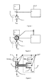
- a detection circuit comprises a photodiode 1 with its internal capacitor 2 .
- the circuit also comprises a biasing circuit 3 which makes it possible to cause the photodiode 1 to swing between a reverse-bias state and a floating state.
- the photodiode 1 is also connected to a readout circuit 4 for processing the signal emitted by the photodiode 1 .
- the charges generated by the photodiode 1 are partly stored into the internal capacitor 2 of the photodiode 1 , which results in a potential variation at the integration node N connected to the readout circuit 4 .
- the electric capacitance of the integration node comes partly from the electric capacitance of the photodiode and partly from the parasitic capacitances of the other elements connected to the integration node N.
- the improvement of the conversion gain of the detector also involves a reduction of the value of the electric capacitance at the integration node of the detection circuit, but the value of the parasitic capacitors generally has the same order of magnitude as that of the capacitor 2 . Thus, there is always an important noise level as for electrons in low-flux detectors.
- FIG. 1 is a schematic representation of a detection circuit of the SFD type
- FIG. 2 is a schematic representation of another detection circuit of the SFD type provided with a shielding
- FIGS. 3 and 4 are schematic representations of two particular embodiments of a detection circuit of the SFD type provided with a shielding
- FIG. 5 is a schematic sectional representation of another detection circuit of the SFD type provided with a shielding between two substrates
- FIG. 6 is a schematic representation of a detection matrix provided with several detection circuits of the SFD type with a shielding.
- the detection circuit of the SFD type (Source-Follower per Detector) comprises a photodetector 1 which is preferentially a photodiode.
- the photodetector 1 is associated with a biasing circuit 3 .
- the biasing circuit 3 makes it possible to bias the photodetector 1 between first and second states. In the first state, the photodetector 1 is reverse biased. In a second state, the photodetector 1 is left in a floating state where it keeps its reverse bias while varying towards the forward bias according to the accumulation of the charges received.
- the photodetector 1 In its floating state, the photodetector 1 transforms a light radiation into an electric charge which is stored into a capacitive retention node called integration node N. In this way, the information received by the photodetector 1 can be stored by the internal capacitance of the photodetector 1 materialized by the integration node N.
- the circuit also comprises a readout circuit 4 which processes the information stored in the integration node N for generating a signal representative of the scene observed by the photodiode in order to send it to a processing circuit (not represented at the output of the readout circuit).
- a readout circuit 4 and the biasing circuit 3 are not perfect, they introduce one or more electric capacitances into the detection circuit in addition to that of the internal capacitor of the photodetector 1 .
- the electric lines used for biasing or for transmitting charges into the circuit also introduce parasitic capacitances.
- the circuit comprises a shielding 5 , preferentially made of metal, which is arranged around the integration node N.
- the shielding 5 physically surrounds the integration node N with one or more screens which are materialized by electrically conducting lines, for example made of metal.
- the shielding forms an electric-field screening or an electromagnetic shielding.
- the shielding 5 is connected to an output of the readout circuit 4 which is configured to have a potential varying in the same direction as the potential of the integration node.
- the potential variation at the shielding 5 and at the integration node N in the same direction makes it possible to reduce the influence of the parasitic capacitances even preferentially to suppress the parasitic capacitances if the potential applied to the shielding follows the potential of the integration node.
- the charges at the terminals of the parasitic capacitances are then constant during the reading because they do no change under their biasing conditions.
- the potential variation in the same direction at the shielding and at the integration node makes it possible to reduce the potential difference between the integration node and the shielding. That makes it possible to reduce the influence of the parasitic capacitances.
- the output of the readout circuit 4 is configured to have a constant potential difference with the value of the integration node N.
- the potential variations at the integration node N are similar to the potential variations at the metal shielding 5 .
- the potential difference between the integration node N and the metal shielding 5 is constant and follows the variations at the integration node N.
- the potential difference between the integration node N and the shielding 5 is constant, that makes it possible to virtually eliminate a part of the parasitic capacitances of the circuit.
- the capacitance value associated with the integration node N then comes close to the value of the capacitance of the photodetector 1 .
- the shielding 5 is arranged at least partially around the line used for biasing the photodetector 1 , i.e. around the line linking the biasing circuit 3 to the photodetector 1 .
- the shielding 5 is arranged around the line which connects the output of the last transistor 6 in the biasing circuit 3 to a first electrode of the photodetector 1 . This embodiment makes it possible to strongly reduce the value of the parasitic capacitance associated with the biasing circuit 3 .
- the shielding 5 is also placed around the last transistor of the biasing circuit 6 in order to reduce the influence of the parasitic capacitances.
- the shielding 5 is at least partially arranged around the line which links the input of the readout circuit 4 to the first electrode of the photodetector 1 as illustrated in FIG. 3 .
- the shielding 5 is also arranged in the readout circuit 4 around one or more transistors enabling the transmission of the information contained in the integration node N ( FIG. 3 ).
- the first transistor of the readout circuit 4 receiving the information from the integration node N is completely surrounded by the shielding in order to strongly reduce the effect of the parasitic capacitances as illustrated in FIG. 3 .
- the readout circuit 4 comprises a follower transistor 7 .
- the readout circuit 4 comprises a follower transistor 7 with an electrode connected to an electric node configured to have a potential which varies in the same direction as the potential at the integration node N.
- the follower transistor 7 includes a control electrode linked to the integration node N and another electrode linked to the output of the readout circuit 4 in a more or less direct way.
- the value of the potential at the integration node N, applied to the control electrode of the follower transistor 7 modifies the value of the signal delivered at the output of the transistor 7 .
- the follower transistor 7 is preferentially a field effect transistor with a gate electrode linked to the integration node and a source/drain electrode linked to the output of the readout circuit 4 .
- the output of the readout circuit 4 is connected to the substrate of the first transistor 6 in the biasing circuit 3 so as to artificially apply the shielding under the channel of the first transistor 6 , which is then a field effect transistor.
- the output of the readout circuit 4 is connected to the substrate of the follower transistor 7 in the readout circuit 4 , which is then a field effect transistor. As previously, that makes it possible to cause the shielding 5 to continue under the channel of the transistor.
- the output of the readout circuit 4 is connected to the substrate of one or more other transistors of the readout circuit 4 .
- the second source/drain electrode of the follower transistor 7 is linked to a first potential Vcell.
- This first potential is variable and follows the variations at the integration node N in order to reduce the influence of the parasitic capacitances.
- the photodetector 1 is made on a first substrate 9 .
- the photodetector 1 is the result of a classic stacking of semiconductor layers for forming for example a junction of the PN type and electrically conducting layers for imposing the potential Vbias.
- the photodetector is represented by a dotted line in the first substrate 9 .
- the biasing circuit 3 and the readout circuit 4 are made on a second substrate 10 .
- the circuits are materialized as an example by the transistors 6 , 7 and 8 .
- the photodetector 1 , the biasing circuit 3 and the readout circuit 4 are connected together by means of a metal bump 11 which carries out the electric connection between the two substrates.
- the shielding 5 comprises a frame 12 around the bump 11 , preferably on the surface of the second substrate and linked to the input of the readout circuit 4 . This embodiment makes it possible to limit the influence of the parasitic capacitances in the hybridization zone.
- the frame 12 forms a ring around the bump 11 .
- the frame 12 is connected to the output of the readout circuit 4 either directly or in the continuity of the shielding 5 .
- the frame 12 comprises a upper part arranged at a predetermined distance around the electrical contact 13 with the bump 11 .
- the frame 12 possibly comprises a lower part arranged on another plane which is arranged facing the insulating zone so as to at least partially cover the insulating zone.
- the frame 12 can be then linked to the shielding 5 by a wide-sized contact opening through the insulating zone or by a multitude of elementary contacts through the insulating layer if the manufacture technology does not allow to open wide-sized contacts.
- the objective is to increase the screenings of the integration node N and of the electric power lines connecting the node N to the bump 11 , to the transistor 6 and to the follower transistor 7 .
- the shielding can be materialized by a more or less continuous ring formed around the node N and the lines.
- the shielding 5 is connected to a source/drain electrode of the transistor 8 .
- the shielding 5 and the frame 12 are preferentially formed in the electric interconnection layers of the circuit in order to be integrated as close to the parasitic capacitances as possible.
- the shielding and the frame are formed in the electric interconnection levels of the second substrate 10 at the same time as the electric power lines connecting the transistors together and to the bump 11 .
- the shielding 5 is arranged in a electrically insulating material, between the bump 11 and the semiconductor substrate comprising the readout circuit 4 .
- the shielding 5 and the frame 12 are formed by one or more electrically conducting materials, for example with doped semiconductor or with metal.
- the shielding and the frame are made out of the same material as the conducting lines connecting the integration node to the various elements of the circuit.
- the shielding and the frame are made out of a metallic material in order to have an important effect on the parasitic capacitances.
- the detection circuit of the SFD type is illustrated as an example with three field effect transistors, but it is also possible to obtain a similar operation with a different number of transistors.
- the photodetector 1 is a photodiode having a first terminal connected to a substrate potential Vbias.
- the second terminal of the photodetector is connected to the biasing circuit 3 which is represented here by a field effect transistor 6 .
- the circuit represented corresponds for example to a circuit of a detection matrix comprising a plurality of circuits.
- the transistor 6 of the biasing circuit 3 is connected between the first biasing terminal applying a reference voltage Vref and the second terminal of the photodetector 1 .
- the second terminal of the photodetector 1 is connected to the input of the readout circuit 4 which is materialized by the gate electrode of the follower transistor 7 .
- the follower transistor 7 and a selecting transistor 8 are connected in series by a first common electrode.
- the second electrode of the follower transistor 7 is connected to a first potential Vcell.
- the second electrode of the selecting transistor 8 is connected to an output line OUT which can be common to several circuits.
- the gate electrode of the selecting transistor 8 is connected to a selecting terminal receiving a selecting signal SEL making it possible to switch the transistor 8 into an on-state or an off-state.
- the integration node N of the circuit is schematized by the common connection between the photodetector 1 , the transistor 6 of the biasing circuit 3 and the follower transistor 7 .
- the charges from the photodetector 1 are stored partly into the internal capacitor of the photodetector 1 and partly into the parasitic capacitors located for example in the transistors used and the metal lines.
- the shielding 5 physically surrounds the integration node N with one or more electric power lines.
- the shielding 5 is also arranged around one of the capacitive components forming the integration node N, for example around the line connecting the biasing transistor 6 to the photodetector 1 and/or around the line connecting the gate electrode of the follower transistor to the photodetector.
- the shielding 5 is arranged around the various parasitic components from the biasing circuit 3 and the readout circuit 4 .
- the substrates of the biasing transistor 4 , the follower transistor 7 and the selecting transistor 8 are connected to the output line OUT so as to have a very strong drop in the parasitic capacitances.
- the biasing circuit 3 and/or the readout circuit 4 are covered by an electrically insulating material inside which one or more metal lines are formed for connecting the various elements together.
- the metal lines are made in the metal interconnection layers of the circuit.
- the metal shielding 5 is made in the interconnection layers of the circuit in order to be placed as close as possible to the metal lines used for transmitting the signal. That makes it possible to have an important effect on the parasitic capacitances.
- the detection circuit can be integrated as a detection matrix with a plurality of detection circuits organized in one or two dimensions.
- the circuits are advantageously connected together by an output line OUT connected to the output terminals of the various readout circuits 4 .
- the detection circuits includes a selecting input in order to avoid the simultaneous flow through two circuits of the same detection line.
- the output line OUT is connected to the metal shielding 5 of its associated circuits.
- the potential of the output line OUT varies with time as the signals from the various circuits flows therethrough.
- the potential of the output line OUT is connected to the potential of the integration node N being read.
- the potential of the output line OUT varies in the same direction as the potential of the integration node N, which makes it possible to limit the influence of the parasitic capacitors.
- the potential difference between the output line OUT and the integration node N are constant during the reading phase.
- the potential of the output line OUT varies with time and moves according to the various integration nodes N, as they are read.
- the photodetector 1 When working, the photodetector 1 is reverse biased by switching the biasing transistor 6 into the on-state.
- the Photodetector 1 is biased between the reference potential Vref and the biasing potential Vbias.
- the biasing transistor 6 is switched into an off-state and the photodetector 1 comes back into a floating state.
- the photodetector 1 converts the light radiation received into a certain amount of electrons representative of the scene observed.
- the variation of the potential at the integration node N represents the signal provided by the photodetector 1 on the scene observed.
- the potential at the integration node N is applied to the control electrode of the follower transistor 7 .
- the potential at the output of the follower transistor 7 (at the first electrode) and the potential at the output of the selecting transistor 8 (at its second electrode) vary in the same direction as the potential at the integration node N.
- the output line OUT receives a signal representative of the scene observed by means of the integration node N.
- the metal shielding 5 placed around the integration node N varies as the potential value at the node N varies, which limits the transfers of electric charges from one reading phase to the following reading phase.
- the value representative of the scene observed is the variation of the potential at the integration node N relative to its initial value.
- the value representative of the scene observed is the variation of the potential at the integration node N between two successive readings, for example with a Correlated Double Sampling technique.
- the metal shielding 5 forms a screening device in the detection circuit what makes it possible to reduce, even to virtually eliminate, the parasitic capacitances.
- the device has then an increased sensitivity performance and a decreased level of noise in term of noise electrons.
Landscapes
- Solid State Image Pick-Up Elements (AREA)
- Transforming Light Signals Into Electric Signals (AREA)
- Light Receiving Elements (AREA)
- Internal Circuitry In Semiconductor Integrated Circuit Devices (AREA)
- Semiconductor Integrated Circuits (AREA)
Abstract
Description
-
- a photodiode connected to an integration node,
- a biasing circuit for biasing the photodiode between a first reverse-bias state and a second floating state,
- a readout circuit connected to the integration node for generating a signal representative of the scene observed by the photodiode,
- a metal shielding arranged around the integration node and connected to an output of the readout circuit, which output is configured to have a potential varying in the same direction as the potential at the integration node.
Claims (11)
Applications Claiming Priority (3)
| Application Number | Priority Date | Filing Date | Title |
|---|---|---|---|
| FR1101571 | 2011-05-20 | ||
| FR1101571A FR2975529B1 (en) | 2011-05-20 | 2011-05-20 | DETECTION CIRCUIT WITH LOW FLOW AND LOW NOISE |
| FR11/01571 | 2011-05-20 |
Publications (2)
| Publication Number | Publication Date |
|---|---|
| US20120292490A1 US20120292490A1 (en) | 2012-11-22 |
| US8872097B2 true US8872097B2 (en) | 2014-10-28 |
Family
ID=46207943
Family Applications (1)
| Application Number | Title | Priority Date | Filing Date |
|---|---|---|---|
| US13/476,444 Active 2033-02-08 US8872097B2 (en) | 2011-05-20 | 2012-05-21 | Low-flux and low-noise detection circuit having a readout circuit with shielded integration node |
Country Status (5)
| Country | Link |
|---|---|
| US (1) | US8872097B2 (en) |
| EP (1) | EP2525406B1 (en) |
| JP (1) | JP6165418B2 (en) |
| FR (1) | FR2975529B1 (en) |
| IL (1) | IL219855A0 (en) |
Cited By (3)
| Publication number | Priority date | Publication date | Assignee | Title |
|---|---|---|---|---|
| DE102020111562A1 (en) | 2020-04-28 | 2021-10-28 | Arnold & Richter Cine Technik Gmbh & Co. Betriebs Kg | Image sensor |
| US20220367555A1 (en) * | 2019-06-26 | 2022-11-17 | Sony Semiconductor Solutions Corporation | Imaging device |
| US11997408B2 (en) | 2021-10-27 | 2024-05-28 | Arnold & Richter Cine Technik Gmbh & Co. Betriebs Kg | Image sensor |
Families Citing this family (4)
| Publication number | Priority date | Publication date | Assignee | Title |
|---|---|---|---|---|
| WO2014002420A1 (en) * | 2012-06-26 | 2014-01-03 | パナソニック株式会社 | Solid-state imaging device |
| US9356061B2 (en) | 2013-08-05 | 2016-05-31 | Apple Inc. | Image sensor with buried light shield and vertical gate |
| US10062722B2 (en) * | 2016-10-04 | 2018-08-28 | Omnivision Technologies, Inc. | Stacked image sensor with shield bumps between interconnects |
| CN219642810U (en) | 2020-08-26 | 2023-09-05 | 株式会社村田制作所 | Electronic component and module |
Citations (7)
| Publication number | Priority date | Publication date | Assignee | Title |
|---|---|---|---|---|
| JPH0758308A (en) | 1993-06-30 | 1995-03-03 | Sanyo Electric Co Ltd | Solid state image pickup element |
| EP0917205A2 (en) | 1997-11-11 | 1999-05-19 | Nec Corporation | High output CMOS-based image sensor |
| US20040223065A1 (en) * | 2003-05-08 | 2004-11-11 | Isao Takayanagi | Wide dynamic range active pixel with knee response |
| US20080054162A1 (en) * | 2006-08-30 | 2008-03-06 | Matsushita Electric Industrial Co., Ltd. | Optical semiconductor device and optical pickup device |
| US20080210846A1 (en) | 2007-02-02 | 2008-09-04 | James Tynan Andrews | Driven light shield for imagers |
| US20100060764A1 (en) | 2008-09-09 | 2010-03-11 | Mccarten John P | High gain read circuit for 3d integrated pixel |
| US20100230729A1 (en) | 2009-03-10 | 2010-09-16 | International Business Machines Corporation | Pixel sensor cell including light shield |
Family Cites Families (2)
| Publication number | Priority date | Publication date | Assignee | Title |
|---|---|---|---|---|
| KR100462164B1 (en) * | 2002-01-11 | 2004-12-17 | 매그나칩 반도체 유한회사 | Cmos image sensor with enhanced fill factor |
| US8253214B2 (en) * | 2005-06-02 | 2012-08-28 | Omnivision Technologies, Inc. | CMOS shared amplifier pixels with output signal wire below floating diffusion interconnect for reduced floating diffusion capacitance |
-
2011
- 2011-05-20 FR FR1101571A patent/FR2975529B1/en not_active Expired - Fee Related
-
2012
- 2012-05-16 EP EP12354029.6A patent/EP2525406B1/en active Active
- 2012-05-17 IL IL219855A patent/IL219855A0/en active IP Right Grant
- 2012-05-18 JP JP2012114265A patent/JP6165418B2/en active Active
- 2012-05-21 US US13/476,444 patent/US8872097B2/en active Active
Patent Citations (7)
| Publication number | Priority date | Publication date | Assignee | Title |
|---|---|---|---|---|
| JPH0758308A (en) | 1993-06-30 | 1995-03-03 | Sanyo Electric Co Ltd | Solid state image pickup element |
| EP0917205A2 (en) | 1997-11-11 | 1999-05-19 | Nec Corporation | High output CMOS-based image sensor |
| US20040223065A1 (en) * | 2003-05-08 | 2004-11-11 | Isao Takayanagi | Wide dynamic range active pixel with knee response |
| US20080054162A1 (en) * | 2006-08-30 | 2008-03-06 | Matsushita Electric Industrial Co., Ltd. | Optical semiconductor device and optical pickup device |
| US20080210846A1 (en) | 2007-02-02 | 2008-09-04 | James Tynan Andrews | Driven light shield for imagers |
| US20100060764A1 (en) | 2008-09-09 | 2010-03-11 | Mccarten John P | High gain read circuit for 3d integrated pixel |
| US20100230729A1 (en) | 2009-03-10 | 2010-09-16 | International Business Machines Corporation | Pixel sensor cell including light shield |
Non-Patent Citations (1)
| Title |
|---|
| Aw et al., "A 128x128-pixel standard-CMOS image sensor with electronic shutter," IEEE International Solid State Circuits Conference, vol. 39, 1996, pp. 180-181 and 440. |
Cited By (6)
| Publication number | Priority date | Publication date | Assignee | Title |
|---|---|---|---|---|
| US20220367555A1 (en) * | 2019-06-26 | 2022-11-17 | Sony Semiconductor Solutions Corporation | Imaging device |
| US11901391B2 (en) * | 2019-06-26 | 2024-02-13 | Sony Semiconductor Solutions Corporation | Imaging device |
| US12183760B2 (en) | 2019-06-26 | 2024-12-31 | Sony Semiconductor Solutions Corporation | Imaging device |
| DE102020111562A1 (en) | 2020-04-28 | 2021-10-28 | Arnold & Richter Cine Technik Gmbh & Co. Betriebs Kg | Image sensor |
| US11563042B2 (en) | 2020-04-28 | 2023-01-24 | Arnold & Richter Cine Technik Gmbh & Co. Betriebs Kg | Image sensor with electrically conductive shielding structure |
| US11997408B2 (en) | 2021-10-27 | 2024-05-28 | Arnold & Richter Cine Technik Gmbh & Co. Betriebs Kg | Image sensor |
Also Published As
| Publication number | Publication date |
|---|---|
| JP2013008952A (en) | 2013-01-10 |
| US20120292490A1 (en) | 2012-11-22 |
| EP2525406B1 (en) | 2018-04-11 |
| IL219855A0 (en) | 2012-07-31 |
| JP6165418B2 (en) | 2017-07-19 |
| FR2975529A1 (en) | 2012-11-23 |
| FR2975529B1 (en) | 2013-09-27 |
| EP2525406A1 (en) | 2012-11-21 |
Similar Documents
| Publication | Publication Date | Title |
|---|---|---|
| US8872097B2 (en) | Low-flux and low-noise detection circuit having a readout circuit with shielded integration node | |
| US20200091213A1 (en) | Solid-state image pickup device and method of driving the same | |
| US9036064B2 (en) | Solid-state imaging device including a photoelectric converting film and camera system using the solid-state imaging device | |
| US10283559B2 (en) | Pixel circuit | |
| KR101565750B1 (en) | High sensitivity image sensor | |
| KR102684972B1 (en) | Image sensor | |
| US9143708B2 (en) | Dual low voltage levels for control of transfer switch device in pixel array | |
| US9848145B2 (en) | Imaging device including pixels | |
| US20190281238A1 (en) | Double source follower hdr pixel | |
| KR101074551B1 (en) | Photo detecting apparatus | |
| US20210185249A1 (en) | Imaging device | |
| CN114363542B (en) | Photosensitive circuit structure and optical devices | |
| US9654714B2 (en) | Shared pixel with fixed conversion gain | |
| CN113395467A (en) | Image sensor with a plurality of pixels | |
| US8018515B2 (en) | Solid-state image pickup device | |
| US8835829B2 (en) | Image sensor formed by silicon rich oxide material | |
| CN101621068A (en) | Image sensor with a plurality of pixels | |
| KR20090043737A (en) | Unit pixel of CMOS image sensor | |
| US7679663B2 (en) | Photodetection apparatus | |
| CN102610623A (en) | Image sensor and source follower | |
| CN114765193B (en) | Image sensing device | |
| KR100977834B1 (en) | CMOS image sensor with wide dynamic range | |
| US12130990B2 (en) | Photoelectric detection circuit, method of controlling photoelectric detection circuit, and pixel unit |
Legal Events
| Date | Code | Title | Description |
|---|---|---|---|
| AS | Assignment |
Owner name: SOCIETE FRANCAISE DE DETECTEURS INFRAROUGES - SOFR Free format text: ASSIGNMENT OF ASSIGNORS INTEREST;ASSIGNOR:SANSON, ERIC;REEL/FRAME:028372/0193 Effective date: 20120523 |
|
| STCF | Information on status: patent grant |
Free format text: PATENTED CASE |
|
| AS | Assignment |
Owner name: SOCIETE FRANCAISE DE DETECTEURS INFRAROUGES-SOFRAD Free format text: CHANGE OF ADDRESS;ASSIGNOR:SOCIETE FRANCAISE DE DETECTEURS INFRAROUGES-SOFRADIR;REEL/FRAME:036385/0291 Effective date: 20140912 |
|
| MAFP | Maintenance fee payment |
Free format text: PAYMENT OF MAINTENANCE FEE, 4TH YEAR, LARGE ENTITY (ORIGINAL EVENT CODE: M1551) Year of fee payment: 4 |
|
| AS | Assignment |
Owner name: LYNRED, FRANCE Free format text: CHANGE OF NAME;ASSIGNOR:SOFRADIR;REEL/FRAME:053844/0652 Effective date: 20190531 |
|
| MAFP | Maintenance fee payment |
Free format text: PAYMENT OF MAINTENANCE FEE, 8TH YEAR, LARGE ENTITY (ORIGINAL EVENT CODE: M1552); ENTITY STATUS OF PATENT OWNER: LARGE ENTITY Year of fee payment: 8 |