US8871635B2 - Integrated circuits and processes for forming integrated circuits having an embedded electrical interconnect within a substrate - Google Patents
Integrated circuits and processes for forming integrated circuits having an embedded electrical interconnect within a substrate Download PDFInfo
- Publication number
- US8871635B2 US8871635B2 US13/466,895 US201213466895A US8871635B2 US 8871635 B2 US8871635 B2 US 8871635B2 US 201213466895 A US201213466895 A US 201213466895A US 8871635 B2 US8871635 B2 US 8871635B2
- Authority
- US
- United States
- Prior art keywords
- layer
- barrier
- recess
- embedded electrical
- over
- Prior art date
- Legal status (The legal status is an assumption and is not a legal conclusion. Google has not performed a legal analysis and makes no representation as to the accuracy of the status listed.)
- Active, expires
Links
- 239000000758 substrate Substances 0.000 title claims abstract description 97
- 238000000034 method Methods 0.000 title claims abstract description 52
- 230000004888 barrier function Effects 0.000 claims abstract description 123
- 239000000463 material Substances 0.000 claims abstract description 51
- 239000004020 conductor Substances 0.000 claims abstract description 31
- 238000005530 etching Methods 0.000 claims description 17
- 238000000151 deposition Methods 0.000 claims description 16
- 239000003989 dielectric material Substances 0.000 claims description 11
- 238000001312 dry etching Methods 0.000 claims description 9
- MZLGASXMSKOWSE-UHFFFAOYSA-N tantalum nitride Chemical compound [Ta]#N MZLGASXMSKOWSE-UHFFFAOYSA-N 0.000 claims description 5
- 238000001039 wet etching Methods 0.000 claims description 5
- 239000000126 substance Substances 0.000 claims description 4
- NRTOMJZYCJJWKI-UHFFFAOYSA-N Titanium nitride Chemical compound [Ti]#N NRTOMJZYCJJWKI-UHFFFAOYSA-N 0.000 claims description 3
- 239000010410 layer Substances 0.000 description 240
- 239000011229 interlayer Substances 0.000 description 12
- 230000015572 biosynthetic process Effects 0.000 description 8
- VYPSYNLAJGMNEJ-UHFFFAOYSA-N Silicium dioxide Chemical compound O=[Si]=O VYPSYNLAJGMNEJ-UHFFFAOYSA-N 0.000 description 7
- 229910021645 metal ion Inorganic materials 0.000 description 7
- BOTDANWDWHJENH-UHFFFAOYSA-N Tetraethyl orthosilicate Chemical compound CCO[Si](OCC)(OCC)OCC BOTDANWDWHJENH-UHFFFAOYSA-N 0.000 description 5
- RYGMFSIKBFXOCR-UHFFFAOYSA-N Copper Chemical compound [Cu] RYGMFSIKBFXOCR-UHFFFAOYSA-N 0.000 description 4
- 238000005229 chemical vapour deposition Methods 0.000 description 4
- 229910052802 copper Inorganic materials 0.000 description 4
- 239000010949 copper Substances 0.000 description 4
- 150000004767 nitrides Chemical class 0.000 description 4
- 229910052715 tantalum Inorganic materials 0.000 description 4
- GUVRBAGPIYLISA-UHFFFAOYSA-N tantalum atom Chemical compound [Ta] GUVRBAGPIYLISA-UHFFFAOYSA-N 0.000 description 4
- KRKNYBCHXYNGOX-UHFFFAOYSA-N citric acid Chemical compound OC(=O)CC(O)(C(O)=O)CC(O)=O KRKNYBCHXYNGOX-UHFFFAOYSA-N 0.000 description 3
- 238000007796 conventional method Methods 0.000 description 3
- 238000009792 diffusion process Methods 0.000 description 3
- 238000010292 electrical insulation Methods 0.000 description 3
- 239000003870 refractory metal Substances 0.000 description 3
- 235000012239 silicon dioxide Nutrition 0.000 description 3
- 239000000377 silicon dioxide Substances 0.000 description 3
- XPDWGBQVDMORPB-UHFFFAOYSA-N Fluoroform Chemical compound FC(F)F XPDWGBQVDMORPB-UHFFFAOYSA-N 0.000 description 2
- 229910052751 metal Inorganic materials 0.000 description 2
- 239000002184 metal Substances 0.000 description 2
- 238000013508 migration Methods 0.000 description 2
- 230000005012 migration Effects 0.000 description 2
- 229910052758 niobium Inorganic materials 0.000 description 2
- 239000010955 niobium Substances 0.000 description 2
- GUCVJGMIXFAOAE-UHFFFAOYSA-N niobium atom Chemical compound [Nb] GUCVJGMIXFAOAE-UHFFFAOYSA-N 0.000 description 2
- 239000002243 precursor Substances 0.000 description 2
- 229910052702 rhenium Inorganic materials 0.000 description 2
- WUAPFZMCVAUBPE-UHFFFAOYSA-N rhenium atom Chemical compound [Re] WUAPFZMCVAUBPE-UHFFFAOYSA-N 0.000 description 2
- 239000004065 semiconductor Substances 0.000 description 2
- 238000012876 topography Methods 0.000 description 2
- WFKWXMTUELFFGS-UHFFFAOYSA-N tungsten Chemical compound [W] WFKWXMTUELFFGS-UHFFFAOYSA-N 0.000 description 2
- 229910052721 tungsten Inorganic materials 0.000 description 2
- 239000010937 tungsten Substances 0.000 description 2
- ZOKXTWBITQBERF-UHFFFAOYSA-N Molybdenum Chemical compound [Mo] ZOKXTWBITQBERF-UHFFFAOYSA-N 0.000 description 1
- KJTLSVCANCCWHF-UHFFFAOYSA-N Ruthenium Chemical compound [Ru] KJTLSVCANCCWHF-UHFFFAOYSA-N 0.000 description 1
- 229910052581 Si3N4 Inorganic materials 0.000 description 1
- 229910004205 SiNX Inorganic materials 0.000 description 1
- RTAQQCXQSZGOHL-UHFFFAOYSA-N Titanium Chemical compound [Ti] RTAQQCXQSZGOHL-UHFFFAOYSA-N 0.000 description 1
- -1 but not limited to Chemical class 0.000 description 1
- 239000003990 capacitor Substances 0.000 description 1
- 230000015556 catabolic process Effects 0.000 description 1
- 229910017052 cobalt Inorganic materials 0.000 description 1
- 239000010941 cobalt Substances 0.000 description 1
- GUTLYIVDDKVIGB-UHFFFAOYSA-N cobalt atom Chemical compound [Co] GUTLYIVDDKVIGB-UHFFFAOYSA-N 0.000 description 1
- 238000004891 communication Methods 0.000 description 1
- 230000003247 decreasing effect Effects 0.000 description 1
- 230000008021 deposition Effects 0.000 description 1
- 238000013461 design Methods 0.000 description 1
- 238000009413 insulation Methods 0.000 description 1
- 238000004519 manufacturing process Methods 0.000 description 1
- 229910044991 metal oxide Inorganic materials 0.000 description 1
- 150000004706 metal oxides Chemical class 0.000 description 1
- 150000002739 metals Chemical class 0.000 description 1
- 229910052750 molybdenum Inorganic materials 0.000 description 1
- 239000011733 molybdenum Substances 0.000 description 1
- 150000002978 peroxides Chemical class 0.000 description 1
- 238000001020 plasma etching Methods 0.000 description 1
- 229920000642 polymer Polymers 0.000 description 1
- 238000012545 processing Methods 0.000 description 1
- 229910052707 ruthenium Inorganic materials 0.000 description 1
- HQVNEWCFYHHQES-UHFFFAOYSA-N silicon nitride Chemical compound N12[Si]34N5[Si]62N3[Si]51N64 HQVNEWCFYHHQES-UHFFFAOYSA-N 0.000 description 1
- 229910052814 silicon oxide Inorganic materials 0.000 description 1
- 238000004528 spin coating Methods 0.000 description 1
- 230000003746 surface roughness Effects 0.000 description 1
- 230000036962 time dependent Effects 0.000 description 1
- 239000010936 titanium Substances 0.000 description 1
- 229910052719 titanium Inorganic materials 0.000 description 1
- 229910052720 vanadium Inorganic materials 0.000 description 1
- LEONUFNNVUYDNQ-UHFFFAOYSA-N vanadium atom Chemical compound [V] LEONUFNNVUYDNQ-UHFFFAOYSA-N 0.000 description 1
Images


Classifications
-
- H—ELECTRICITY
- H01—ELECTRIC ELEMENTS
- H01L—SEMICONDUCTOR DEVICES NOT COVERED BY CLASS H10
- H01L21/00—Processes or apparatus adapted for the manufacture or treatment of semiconductor or solid state devices or of parts thereof
- H01L21/70—Manufacture or treatment of devices consisting of a plurality of solid state components formed in or on a common substrate or of parts thereof; Manufacture of integrated circuit devices or of parts thereof
- H01L21/71—Manufacture of specific parts of devices defined in group H01L21/70
- H01L21/768—Applying interconnections to be used for carrying current between separate components within a device comprising conductors and dielectrics
- H01L21/76838—Applying interconnections to be used for carrying current between separate components within a device comprising conductors and dielectrics characterised by the formation and the after-treatment of the conductors
- H01L21/76877—Filling of holes, grooves or trenches, e.g. vias, with conductive material
- H01L21/76883—Post-treatment or after-treatment of the conductive material
-
- H—ELECTRICITY
- H01—ELECTRIC ELEMENTS
- H01L—SEMICONDUCTOR DEVICES NOT COVERED BY CLASS H10
- H01L21/00—Processes or apparatus adapted for the manufacture or treatment of semiconductor or solid state devices or of parts thereof
- H01L21/70—Manufacture or treatment of devices consisting of a plurality of solid state components formed in or on a common substrate or of parts thereof; Manufacture of integrated circuit devices or of parts thereof
- H01L21/71—Manufacture of specific parts of devices defined in group H01L21/70
- H01L21/768—Applying interconnections to be used for carrying current between separate components within a device comprising conductors and dielectrics
- H01L21/76801—Applying interconnections to be used for carrying current between separate components within a device comprising conductors and dielectrics characterised by the formation and the after-treatment of the dielectrics, e.g. smoothing
- H01L21/76829—Applying interconnections to be used for carrying current between separate components within a device comprising conductors and dielectrics characterised by the formation and the after-treatment of the dielectrics, e.g. smoothing characterised by the formation of thin functional dielectric layers, e.g. dielectric etch-stop, barrier, capping or liner layers
- H01L21/76832—Multiple layers
-
- H—ELECTRICITY
- H01—ELECTRIC ELEMENTS
- H01L—SEMICONDUCTOR DEVICES NOT COVERED BY CLASS H10
- H01L21/00—Processes or apparatus adapted for the manufacture or treatment of semiconductor or solid state devices or of parts thereof
- H01L21/70—Manufacture or treatment of devices consisting of a plurality of solid state components formed in or on a common substrate or of parts thereof; Manufacture of integrated circuit devices or of parts thereof
- H01L21/71—Manufacture of specific parts of devices defined in group H01L21/70
- H01L21/768—Applying interconnections to be used for carrying current between separate components within a device comprising conductors and dielectrics
- H01L21/76801—Applying interconnections to be used for carrying current between separate components within a device comprising conductors and dielectrics characterised by the formation and the after-treatment of the dielectrics, e.g. smoothing
- H01L21/76829—Applying interconnections to be used for carrying current between separate components within a device comprising conductors and dielectrics characterised by the formation and the after-treatment of the dielectrics, e.g. smoothing characterised by the formation of thin functional dielectric layers, e.g. dielectric etch-stop, barrier, capping or liner layers
- H01L21/76834—Applying interconnections to be used for carrying current between separate components within a device comprising conductors and dielectrics characterised by the formation and the after-treatment of the dielectrics, e.g. smoothing characterised by the formation of thin functional dielectric layers, e.g. dielectric etch-stop, barrier, capping or liner layers formation of thin insulating films on the sidewalls or on top of conductors
-
- H—ELECTRICITY
- H01—ELECTRIC ELEMENTS
- H01L—SEMICONDUCTOR DEVICES NOT COVERED BY CLASS H10
- H01L21/00—Processes or apparatus adapted for the manufacture or treatment of semiconductor or solid state devices or of parts thereof
- H01L21/70—Manufacture or treatment of devices consisting of a plurality of solid state components formed in or on a common substrate or of parts thereof; Manufacture of integrated circuit devices or of parts thereof
- H01L21/71—Manufacture of specific parts of devices defined in group H01L21/70
- H01L21/768—Applying interconnections to be used for carrying current between separate components within a device comprising conductors and dielectrics
- H01L21/76838—Applying interconnections to be used for carrying current between separate components within a device comprising conductors and dielectrics characterised by the formation and the after-treatment of the conductors
- H01L21/76841—Barrier, adhesion or liner layers
- H01L21/76853—Barrier, adhesion or liner layers characterized by particular after-treatment steps
- H01L21/76865—Selective removal of parts of the layer
Definitions
- the present invention generally relates to integrated circuits and processes for forming integrated circuits having an embedded electrical interconnect within a substrate of the integrated circuit. More particularly, the present invention relates to integrated circuits and processes for forming integrated circuits having an embedded electrical interconnect recessed within a substrate and with a barrier layer disposed between the embedded electrical interconnect and the substrate.
- microprocessor integrated circuits generally include numerous levels of interconnect routing in the form of electrical interconnects, such as lines and dots, embedded within a dielectric substrate to connect transistors within the integrated circuits.
- Each level of interconnect routing is separated from immediately adjacent levels by the dielectric material, referred to in the art as an interlayer dielectric (ILD).
- the ILD generally includes an oxide layer that includes an oxide, such as silicon dioxide formed from tetraethyl orthosilicate (TEOS), and may include one or more additional layers of dielectric material such as low-k or ultra-low k (ULK) material.
- TEOS tetraethyl orthosilicate
- ULK ultra-low k
- Adjacent levels of interconnect routing may be embedded in distinct layers of ILD, and with the interconnect routing configured in such a way so as to ensure that dielectric material separates the adjacent interconnect routings.
- the embedded electrical interconnects in the interconnect routing can be selectively insulated from both other embedded electrical interconnects in the same interconnect routing and from embedded electrical interconnects in interconnect routing of adjacent levels.
- embedded electrical interconnects in adjacent levels of interconnect routing can also be selectively connected to fabricate desired circuitry in the integrated circuits.
- TDDB time dependent dielectric breakdown
- a layer of ILD is formed over a base substrate, which may be a semiconductor substrate or another level of interconnect routing.
- Trenches and/or vias are etched into the ILD, followed by deposition of an electrically-conductive material into the trenches and/or vias. Excess electrically-conductive material is removed through chemical and/or mechanical removal techniques to define the interconnect routing of embedded electrical interconnects. Wet etch techniques are then employed to etch electrically-conductive material from the exposed surfaces of the embedded electrical interconnects to thereby recess the embedded electrical interconnects within the ILD prior to forming additional layers thereon.
- a barrier layer is often formed in the trenches and/or vias prior to depositing the electrically-conductive material in the trenches and/or vias.
- the barrier layer generally includes a barrier material such as tantalum nitride.
- a liner layer of liner material such as tantalum may be formed over the barrier layer prior to depositing the electrically-conductive material in the trenches and/or vias to further assist as a barrier to flow of metal ions into the interface. Recessing of the barrier layer and the liner layer within the substrate is desirable to promote electrical insulation of the embedded electrical interconnects and to further minimize TDDB.
- wet etch techniques that are employed to remove electrically-conductive material from the exposed surfaces of the embedded electrical interconnects do not etch the barrier material at the same rate as the electrically-conductive material.
- dry etch techniques that are generally effective for etching tantalum nitride and tantalum also etch the oxide layer in the ILD at a high rate, which gives rise to reliability concerns in the integrated circuit by causing uneven topography, reducing the volume of ILD that separates the interconnect routing, and breaking down the oxide layer.
- a process for forming an integrated circuit includes providing a substrate including an oxide layer and a protecting layer disposed over the oxide layer. A recess is etched through the protecting layer and at least partially into the oxide layer. A barrier material is deposited in the recess to form a barrier layer over the protecting layer and the oxide layer in the recess. An electrically-conductive material different from the barrier material is deposited over the barrier layer in the recess to form an embedded electrical interconnect. The embedded electrical interconnect is recessed to an interconnect recess depth within the substrate.
- the barrier layer is recessed to a barrier recess depth within the substrate after recessing the embedded electrical interconnect, and at least a portion of the protecting layer remains over the oxide layer after recessing the barrier layer.
- the protecting layer is removed from the oxide layer after recessing the barrier layer.
- a process for forming an integrated circuit includes providing a substrate including an underlying dielectric layer, an oxide layer disposed over the underlying dielectric layer, and a protecting layer disposed over the oxide layer.
- a recess is etched through the protecting layer, at least partially into the oxide layer, and optionally at least partially into the underlying dielectric layer.
- a barrier material is deposited in the recess to form a barrier layer over the protecting layer, the oxide layer, and optionally the underlying dielectric layer in the recess.
- a liner material different from the barrier material is deposited over the barrier layer in the recess to form a liner layer.
- An electrically-conductive material is deposited over the liner layer in the recess to form an embedded electrical interconnect.
- the embedded electrical interconnect is wet etched to an interconnect recess depth within the substrate.
- the barrier layer is dry etched to a barrier recess depth within the substrate after recessing the embedded electrical interconnect. At least a portion of the protecting layer remains over the oxide layer after recessing the barrier layer. The protecting layer is removed from the oxide layer after recessing the barrier layer.
- an integrated circuit in another embodiment, includes a base substrate and an interlayer dielectric substrate disposed over the base substrate.
- the interlayer dielectric substrate has an embedded electrical interconnect disposed therein and a barrier layer disposed between the embedded electrical interconnect and the interlayer dielectric substrate.
- the embedded electrical interconnect and barrier layer are recessed within the interlayer dielectric substrate and have a recessed interconnect surface and a recessed barrier surface, respectively.
- the recessed barrier surface is on common plane with the recessed interconnect surface.
- FIG. 1 is a schematic cross-sectional side view of a portion of an integrated circuit including a base substrate, an underlying dielectric layer, an oxide layer, and a protecting layer;
- FIG. 2A is a schematic cross-sectional side view of a portion of the integrated circuit of FIG. 1 including an etch mask patterned over the protecting layer, with the etch mask having a patterned recess and with a recess etched through the protecting layer and the oxide layer and partially into the underlying dielectric layer;
- FIG. 2B is a schematic cross-sectional side view of a portion of the integrated circuit of FIG. 1 including an etch mask patterned over the protecting layer, with the etch mask having a patterned recess and with a recess etched through the protecting layer, the oxide layer, and the underlying dielectric layer;
- FIG. 3 is a schematic cross-sectional side view of a portion of the integrated circuit of FIG. 2A including the recess, with a barrier material, a liner material, and an electrically-conductive material deposited over the protecting layer and in the recess to form a barrier layer, liner layer, and embedded electrical interconnect, respectfully, in the recess;
- FIG. 4 is a schematic cross-sectional side view of a portion of the integrated circuit of FIG. 3 after removal of excess barrier material, liner material, and electrically-conductive material from the protecting layer;
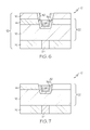
- FIG. 5 is a schematic cross-sectional side view of a portion of the integrated circuit of FIG. 4 , with the embedded electrical interconnect recessed within the substrate;
- FIG. 6 is a schematic cross-sectional side view of a portion of the integrated circuit of FIG. 5 , with the barrier layer and liner layer recessed within the substrate;
- FIG. 7 is a schematic cross-sectional side view of a portion of the integrated circuit of FIG. 6 , after removal of the protecting layer;
- FIG. 8 is a schematic cross-sectional side view of a portion of the integrated circuit of FIG. 7 , with a capping layer and an NBLoK layer formed over the embedded electrical interconnect and the oxide layer;
- FIG. 9 is a schematic cross-sectional side view of a portion of the integrated circuit of FIG. 8 , with an overlying substrate having another embedded electrical interconnect formed over the capping layer and NBLoK layer;
- FIG. 10 is a schematic cross-sectional side view of a portion of an embodiment of an integrated circuit prepared in accordance with the processes described herein.
- Integrated circuits and processes for forming integrated circuits are provided herein.
- the processes involve formation of integrated circuits having an embedded electrical interconnect in a substrate of the integrated circuits when a barrier layer is disposed between the embedded electrical interconnect and the substrate and when the substrate includes an oxide layer.
- the processes allow the embedded electrical interconnect and the barrier layer to be effectively recessed within the substrate while minimizing etching of the oxide layer.
- a protecting layer is disposed over the oxide layer during recessing of the embedded electrical interconnect and the barrier layer within the substrate, and at least a portion of the protecting layer remains over the oxide layer after recessing the barrier layer. In this manner, etching techniques that preferentially etch the barrier layer can be employed to recess the barrier layer.
- etching techniques that preferentially etch the barrier layer may otherwise etch the oxide layer at a high rate, thereby breaking down and causing uneven topography of the oxide layer, etching of the oxide layer is minimized because the oxide layer is at least partially shielded from etching by the protecting layer.
- the protecting layer is removed after recessing the barrier layer.
- the embedded electrical interconnect and the barrier layer can be recessed to recess depths that are on a common plane, which promotes further layer formation over the recessed embedded electrical interconnect and barrier layer and which further results in maximized electrical insulation of the embedded electrical interconnect and barrier layer.
- the processes for forming integrated circuits, as described herein, are particularly useful for recessing embedded electrical interconnects and barrier layers within an interlayer dielectric substrate of an integrated circuit due to the maximized electrical insulation and promotion of further layer formation that is afforded by the processes.
- the process includes providing the substrate 12 that includes an oxide layer 14 and a protecting layer 16 that is disposed over the oxide layer 14 .
- the substrate 12 further includes an underlying dielectric layer 18 , with the oxide layer 14 disposed over the underlying dielectric layer 18 .
- the substrate 12 may optionally include a base substrate 20 , with the underlying dielectric layer 18 disposed over the base substrate 20 .
- the oxide layer 14 and optional underlying dielectric layer 18 may be referred to as an interlayer dielectric substrate 22 .
- the oxide layer 14 is provided with the protecting layer 16 disposed directly thereon, with the oxide layer 14 disposed directly on the underlying dielectric layer 18 , and with the underlying dielectric layer 18 disposed directly on the base substrate 20 .
- additional layers can be disposed between the oxide layer 14 and the protecting layer 16 , between the oxide layer 14 and the underlying dielectric layer 18 , and/or between the underlying dielectric layer 18 and the base substrate 20 .
- the oxide layer 14 , protecting layer 16 , underlying dielectric layer 18 , and the base substrate 20 are generally configured in a stacked orientation.
- the base substrate 20 may have an embedded electrical contact 24 disposed therein, and may include millions of embedded electrical contacts 24 disposed therein.
- the embedded electrical contacts 24 may be formed with nanometer-scale dimensions, e.g., with dimensions less than 1 ⁇ 10 ⁇ 6 mm.
- the base substrate 20 may be a base dielectric substrate 12 including the embedded electrical contact 24 disposed therein, and may be formed from any dielectric material or may include layers of different dielectric materials.
- the base substrate 20 may be a semiconductor substrate 12 that includes a device, such as a transistor, capacitor, resistor, or the like, with the embedded electrical contact 24 being in electrical communication with the device.
- the base substrate 20 may be free of embedded electrical contacts 24 disposed therein and may be any substrate 12 upon which subsequent layers of dielectric material may be formed.
- the optional underlying dielectric layer 18 can be formed from a low k or ultra-low k dielectric material, such as a silsesquioxane polymer, so long as the material used to form the underlying dielectric layer 18 is different from the material used to form the oxide layer 14 .
- a low k or ultra-low k dielectric material such as a silsesquioxane polymer
- Such low k or ultra-low k dielectric materials are known in the art and are particularly useful when the instant process is utilized to form integrated circuits 10 as shown in FIG. 10 .
- the underlying dielectric layer 18 may be formed over the base substrate 20 through conventional techniques such as spin coating.
- the oxide layer 14 can be formed from any insulating oxide, and is typically formed from a silicon oxide, such as silicon dioxide.
- a silicon oxide such as silicon dioxide.
- TEOS tetraethyl orthosilicate
- Formation of oxide layers using TEOS precursor is known in the art, and such oxide layers may be formed through conventional techniques such as chemical vapor deposition (CVD).
- the protecting layer 16 is not particularly limited and is a sacrificial layer that is present for purposes of shielding the oxide layer 14 from processing techniques that are conducted in accordance with the instant process that would otherwise degrade or remove material from the oxide layer 14 .
- the protecting layer 16 can be formed from material that exhibits a slower etch rate in a dry etchant than the material used to form the oxide layer 14 .
- the protecting layer 16 is formed from material that has a higher wet etch rate than dry etch rate.
- the protecting layer 16 includes titanium nitride and can be formed through conventional techniques such as chemical vapor deposition (CVD).
- the exemplary process continues with etching a recess 26 through the protecting layer 16 and at least partially into the oxide layer 14 as shown in FIGS. 2A and 2B .
- a plurality of recesses 26 can be etched.
- an etch mask 28 may be formed and patterned over the protecting layer 16 , with the etch mask 28 having patterned recesses 30 that selectively expose a surface of the protecting layer 16 .
- the recess 26 is then etched through the protecting layer 16 and at least partially into the oxide layer 14 through the patterned recesses 30 in the etch mask 28 , with multiple cycles of etching conducted with appropriate etchants for at least the protecting layer 16 and the oxide layer 14 .
- the recess 26 is etched through the oxide layer 14 and at least partially into the underlying dielectric layer 18 .
- the recess 26 is etched through the protecting layer 16 , the oxide layer 14 , and only partially into the underlying dielectric layer 18 and illustrates formation of the recess 26 in a trench configuration.
- the recess 26 is a via 26 and is etched through the protecting layer 16 , the oxide layer 14 , and the underlying dielectric layer 18 .
- the protecting layer 16 includes titanium nitride
- dry etching using etchants such as, but not limited to, CHF 3 , CF 4 , or SF 6
- etchants such as, but not limited to, CHF 3 , CF 4 , or SF 6
- the via 26 is etched over the embedded electrical contact 24 that is disposed in the base substrate 20 and exposes a surface of the embedded electrical contact 24 .
- a barrier material is deposited in the recess 26 to form a barrier layer 32 over the protecting layer 16 and oxide layer 14 in the recess 26 , followed by depositing an electrically-conductive material over the barrier layer 32 in the recess 26 to form an embedded electrical interconnect 34 .
- the barrier layer 32 functions as a barrier to diffusion of metal ions from the electrically-conductive material of the embedded electrical interconnect 34 into an interface between layers in the substrate 12 .
- a liner material may be deposited over the barrier layer 32 in the recess 26 to form a liner layer 36 , which provides a further barrier to diffusion of the metal ions.
- the electrically-conductive material is deposited over the liner layer 36 .
- the electrically-conductive material is deposited directly upon the liner layer 36 .
- the barrier material, the liner material, and the electrically-conductive material are generally uniformly deposited over the substrate 12 , including over the surface of the protecting layer 16 in addition to depositing in the recess 26 .
- the barrier layer 32 is generally formed from a barrier material that is different from materials that are used to form the protecting layer 16 , the oxide layer 14 , and the optional underlying dielectric layer 18 .
- the barrier material is a refractory metal nitride, such as a nitride of niobium, molybdenum, tantalum, tungsten, or rhenium.
- Refractory metal nitrides provide excellent diffusion barrier properties and that also exhibits chemical stability and high electrical conductivity.
- a suitable refractory metal nitride that is suitable for the barrier material is tantalum nitride.
- the liner material is different from the barrier material and, in an embodiment, is chosen from, but is not limited to, elemental tantalum, cobalt, rhenium, niobium, vanadium, ruthenium, or a combination thereof.
- the electrically-conductive material is different from the barrier material and liner material and has sufficient electrical conductivity to facilitate electrical connection in a circuit, e.g., with electrical resistivity of less than or equal to about 30 ⁇ cm.
- suitable electrically-conductive materials include metals such as, but not limited to, copper, titanium, or tungsten.
- the electrically-conductive material is substantially pure copper (e.g., at least about 99% pure) and may be electronics grade copper that is suitable for sensitive circuitry of integrated circuits 10 .
- the embedded electrical interconnect 34 is in the form of one or more dots and/or lines, depending upon a pattern of recesses 26 formed in the substrate 12 .
- CMP Chemical mechanical planarization
- the process continues with recessing the embedded electrical interconnect 34 within the substrate 12 .
- the embedded electrical interconnect 34 is recessed by wet etching the embedded electrical interconnect 34 .
- An appropriate wet etchant may be used to wet etch the embedded electrical interconnect 34 , such as Standard Clean 1 (SC1), Standard Clean 2 (SC2), or other peroxide based chemistries to oxidize the metal followed by HF or citric acid to remove the metal oxide layer.
- SC1 Standard Clean 1
- SC2 Standard Clean 2
- the embedded electrical interconnect 34 is recessed to an interconnect recess depth 38 , and etching may be conducted until a desired interconnect recess depth 38 is achieved.
- the interconnect recess depth 38 is at least beneath a surface plane 39 of the oxide layer 14 , thereby offsetting the embedded electrical interconnect 34 from the surface plane 39 of the oxide layer 14 and effectively forming a barrier to flow of metal ions from the embedded electrical interconnect 34 into the interface between the oxide layer 14 and a subsequently formed capping layer (as described in further detail below).
- the interconnect recess depth 38 is at least 4 nm beneath the surface plane 39 of the oxide layer 14 .
- the barrier layer 32 is recessed within the substrate 12 .
- the barrier material and the liner material generally have a lower etch rate in the wet etchant than the electrically-conductive material such that wet etching is insufficient to effectively etch the barrier material and liner material (when present).
- the barrier layer 32 and the liner layer 36 are recessed by dry etching. Dry etching is also referred to in the art as plasma etching and examples of suitable etchants that can be used in dry etching include, but are not limited to, CHF 3 , CF 4 , or SF 6 .
- the oxide layer 14 is vulnerable to etch if exposed to dry etching.
- the protecting layer 16 is still present over the oxide layer 14 during recessing of the embedded electrical interconnect 34 and the barrier layer 32 .
- at least a portion of the protecting layer 16 remains over the oxide layer 14 after recessing the barrier layer 32 to ensure that the oxide layer 14 is sufficiently shielded from exposure to dry etching.
- the barrier layer 32 and, when present, the liner layer 36 are recessed to a barrier recess depth 40 .
- the barrier recess depth 40 is on common plane with the interconnect recess depth 38 .
- common plane it is meant that the barrier recess depth 40 and the interconnect recess depth 38 have an offset of less than about 2 nm, such as from an equal plane to an offset of about 7 nm.
- the protecting layer 16 is removed from the oxide layer 14 as shown in FIG. 7 .
- Techniques for removing the protecting layer 16 are not particularly limited and can include CMP or wet etching, thereby exposing a surface of the oxide layer 14 .
- a capping layer 42 is formed over the embedded electrical interconnect 34 and barrier layer 32 after recessing the embedded electrical interconnect 34 and barrier layer 32 and after removing the protecting layer 16 .
- the capping layer 42 is typically formed from a dielectric material and serves to passivate the embedded electrical interconnect 34 within the substrate 12 .
- the capping layer 42 includes silicon nitride and is formed directly over the oxide layer 14 , the embedded electrical interconnect 34 , and the barrier layer 32 , followed by formation of a SiN x C y H z layer 44 (referred to in the art as NBLoK; shown in FIG. 8 ). As shown in FIG.
- the capping layer 42 and the NBLoK layer 44 that are formed over the embedded electrical interconnect 34 may be considered part of the interlayer dielectric substrate 22 as the capping layer 42 may serve to electrically isolate the embedded electrical interconnect 34 from other embedded electrical interconnects 34 that may subsequently be formed in additional overlaying substrates 46 , and the NBLoK layer 44 may serve to provide further dielectric insulation between the embedded electrical interconnect 34 and the additional overlaying substrate 12 as well as to provide etch-stop functions during formation of recesses as vias in the additional overlaying substrate 12 .
- the capping layer 42 and NBLoK layer 44 may perform other functions as may be desirable in accordance with design considerations.
- an overlying substrate 46 having another embedded electrical interconnect 34 may be formed over the capping layer 42 (more specifically, directly over the NBLoK layer 44 ).
- the integrated circuit 10 includes a base substrate 20 and an interlayer dielectric substrate 22 disposed over the base substrate 20 .
- the interlayer dielectric substrate 22 has an embedded electrical interconnect 34 disposed therein and a barrier layer 32 disposed between the embedded electrical interconnect 34 and the interlayer dielectric substrate 22 .
- the embedded electrical interconnect 34 and the barrier layer 32 are recessed within the interlayer dielectric substrate 22 and have a recessed interconnect surface 48 and a recessed barrier surface 50 , respectively.
- the recessed barrier surface 50 is on common plane with the recessed interconnect surface 48 .
- the integrated circuit 10 may include a capping layer 42 disposed over and in contact with the embedded electrical interconnect 34 .
- An overlying substrate 46 having another embedded electrical interconnect 34 disposed therein may be disposed over the capping layer 42 .
- the integrated circuit 10 can be prepared in accordance with the processes described herein, the integrated circuits are not so limited and can be prepared in accordance with other processes so long as the above-described surface roughness of the recessed surface in the embedded copper interconnect is achieved.
Landscapes
- Engineering & Computer Science (AREA)
- Physics & Mathematics (AREA)
- Condensed Matter Physics & Semiconductors (AREA)
- General Physics & Mathematics (AREA)
- Manufacturing & Machinery (AREA)
- Computer Hardware Design (AREA)
- Microelectronics & Electronic Packaging (AREA)
- Power Engineering (AREA)
- Internal Circuitry In Semiconductor Integrated Circuit Devices (AREA)
Abstract
Description
Claims (17)
Priority Applications (1)
| Application Number | Priority Date | Filing Date | Title |
|---|---|---|---|
| US13/466,895 US8871635B2 (en) | 2012-05-08 | 2012-05-08 | Integrated circuits and processes for forming integrated circuits having an embedded electrical interconnect within a substrate |
Applications Claiming Priority (1)
| Application Number | Priority Date | Filing Date | Title |
|---|---|---|---|
| US13/466,895 US8871635B2 (en) | 2012-05-08 | 2012-05-08 | Integrated circuits and processes for forming integrated circuits having an embedded electrical interconnect within a substrate |
Publications (2)
| Publication Number | Publication Date |
|---|---|
| US20130299994A1 US20130299994A1 (en) | 2013-11-14 |
| US8871635B2 true US8871635B2 (en) | 2014-10-28 |
Family
ID=49548025
Family Applications (1)
| Application Number | Title | Priority Date | Filing Date |
|---|---|---|---|
| US13/466,895 Active 2032-05-29 US8871635B2 (en) | 2012-05-08 | 2012-05-08 | Integrated circuits and processes for forming integrated circuits having an embedded electrical interconnect within a substrate |
Country Status (1)
| Country | Link |
|---|---|
| US (1) | US8871635B2 (en) |
Cited By (2)
| Publication number | Priority date | Publication date | Assignee | Title |
|---|---|---|---|---|
| US20190148289A1 (en) * | 2017-11-15 | 2019-05-16 | Samsung Electronics Co., Ltd. | Semiconductor device and method for fabricating the same |
| US10699945B2 (en) | 2018-10-04 | 2020-06-30 | International Business Machines Corporation | Back end of line integration for interconnects |
Families Citing this family (8)
| Publication number | Priority date | Publication date | Assignee | Title |
|---|---|---|---|---|
| US9236411B2 (en) * | 2011-08-03 | 2016-01-12 | Omnivision Technologies, Inc. | Color filter patterning using hard mask |
| JP5673627B2 (en) * | 2012-08-03 | 2015-02-18 | トヨタ自動車株式会社 | Semiconductor device and manufacturing method thereof |
| US9620589B2 (en) | 2014-04-07 | 2017-04-11 | GlobalFoundries, Inc. | Integrated circuits and methods of fabrication thereof |
| CN104979329B (en) * | 2014-04-10 | 2018-08-10 | 中芯国际集成电路制造(上海)有限公司 | A kind of semiconductor devices and its manufacturing method and electronic device |
| US9685406B1 (en) | 2016-04-18 | 2017-06-20 | International Business Machines Corporation | Selective and non-selective barrier layer wet removal |
| US10431464B2 (en) | 2016-10-17 | 2019-10-01 | International Business Machines Corporation | Liner planarization-free process flow for fabricating metallic interconnect structures |
| US10672653B2 (en) | 2017-12-18 | 2020-06-02 | International Business Machines Corporation | Metallic interconnect structures with wrap around capping layers |
| US20230275121A1 (en) * | 2022-02-28 | 2023-08-31 | Taiwan Semiconductor Manufacturing Company Limited | Semiconductor structure and method of manufacture |
Citations (11)
| Publication number | Priority date | Publication date | Assignee | Title |
|---|---|---|---|---|
| US5173438A (en) * | 1991-02-13 | 1992-12-22 | Micron Technology, Inc. | Method of performing a field implant subsequent to field oxide fabrication by utilizing selective tungsten deposition to produce encroachment-free isolation |
| US6004188A (en) * | 1998-09-10 | 1999-12-21 | Chartered Semiconductor Manufacturing Ltd. | Method for forming copper damascene structures by using a dual CMP barrier layer |
| US6191029B1 (en) * | 1999-09-09 | 2001-02-20 | United Silicon Incorporated | Damascene process |
| US20030003711A1 (en) * | 2001-06-29 | 2003-01-02 | Anjaneya Modak | Method of making a semiconductor device with aluminum capped copper interconnect pads |
| US6774041B1 (en) * | 1999-12-27 | 2004-08-10 | Renesas Technology Corp. | Polishing method, metallization fabrication method, method for manufacturing semiconductor device and semiconductor device |
| US20070155165A1 (en) * | 2005-12-30 | 2007-07-05 | Samsung Electronics Co., Ltd. | Methods for forming damascene wiring structures having line and plug conductors formed from different materials |
| US20080171447A1 (en) | 2007-01-12 | 2008-07-17 | Advanced Micro Devices, Inc. | Method of forming semiconductor device with multiple level patterning |
| US20090023298A1 (en) | 2007-07-17 | 2009-01-22 | Advanced Micro Devices, Inc. | Inverse self-aligned spacer lithography |
| US20090283907A1 (en) * | 2008-05-13 | 2009-11-19 | Micron Technology, Inc. | Low-resistance interconnects and methods of making same |
| US20110097896A1 (en) * | 2002-09-04 | 2011-04-28 | Koninklijke Philips Electronics N.V. | Method for fabrication of in-laid metal interconnects |
| US8232200B1 (en) * | 2011-03-18 | 2012-07-31 | International Business Machines Corporation | Methods of forming integrated circuit devices having damascene interconnects therein with metal diffusion barrier layers and devices formed thereby |
-
2012
- 2012-05-08 US US13/466,895 patent/US8871635B2/en active Active
Patent Citations (11)
| Publication number | Priority date | Publication date | Assignee | Title |
|---|---|---|---|---|
| US5173438A (en) * | 1991-02-13 | 1992-12-22 | Micron Technology, Inc. | Method of performing a field implant subsequent to field oxide fabrication by utilizing selective tungsten deposition to produce encroachment-free isolation |
| US6004188A (en) * | 1998-09-10 | 1999-12-21 | Chartered Semiconductor Manufacturing Ltd. | Method for forming copper damascene structures by using a dual CMP barrier layer |
| US6191029B1 (en) * | 1999-09-09 | 2001-02-20 | United Silicon Incorporated | Damascene process |
| US6774041B1 (en) * | 1999-12-27 | 2004-08-10 | Renesas Technology Corp. | Polishing method, metallization fabrication method, method for manufacturing semiconductor device and semiconductor device |
| US20030003711A1 (en) * | 2001-06-29 | 2003-01-02 | Anjaneya Modak | Method of making a semiconductor device with aluminum capped copper interconnect pads |
| US20110097896A1 (en) * | 2002-09-04 | 2011-04-28 | Koninklijke Philips Electronics N.V. | Method for fabrication of in-laid metal interconnects |
| US20070155165A1 (en) * | 2005-12-30 | 2007-07-05 | Samsung Electronics Co., Ltd. | Methods for forming damascene wiring structures having line and plug conductors formed from different materials |
| US20080171447A1 (en) | 2007-01-12 | 2008-07-17 | Advanced Micro Devices, Inc. | Method of forming semiconductor device with multiple level patterning |
| US20090023298A1 (en) | 2007-07-17 | 2009-01-22 | Advanced Micro Devices, Inc. | Inverse self-aligned spacer lithography |
| US20090283907A1 (en) * | 2008-05-13 | 2009-11-19 | Micron Technology, Inc. | Low-resistance interconnects and methods of making same |
| US8232200B1 (en) * | 2011-03-18 | 2012-07-31 | International Business Machines Corporation | Methods of forming integrated circuit devices having damascene interconnects therein with metal diffusion barrier layers and devices formed thereby |
Non-Patent Citations (3)
| Title |
|---|
| Lu et al., "Reproductible Resistive-Switching Behavior in Copper-Nitride Thin Film Prepared by Plasma-Immersion Ion Implantation," Phys. Status Solidi A 208, No. 4, pp. 874-877, (2011). |
| Nosaka et al., "Thermal Decomposition of Copper Nitride Thin Films and Dots Formation by Electron Beam Writing," Applied Surface Science, 169-170, pp. 358-361, (2001). |
| U.S. Appl. No. 13/362,981, filed Jan. 31, 2012. |
Cited By (3)
| Publication number | Priority date | Publication date | Assignee | Title |
|---|---|---|---|---|
| US20190148289A1 (en) * | 2017-11-15 | 2019-05-16 | Samsung Electronics Co., Ltd. | Semiconductor device and method for fabricating the same |
| US10535600B2 (en) * | 2017-11-15 | 2020-01-14 | Samsung Electronics Co., Ltd. | Semiconductor device |
| US10699945B2 (en) | 2018-10-04 | 2020-06-30 | International Business Machines Corporation | Back end of line integration for interconnects |
Also Published As
| Publication number | Publication date |
|---|---|
| US20130299994A1 (en) | 2013-11-14 |
Similar Documents
| Publication | Publication Date | Title |
|---|---|---|
| US8871635B2 (en) | Integrated circuits and processes for forming integrated circuits having an embedded electrical interconnect within a substrate | |
| US7550822B2 (en) | Dual-damascene metal wiring patterns for integrated circuit devices | |
| US8138082B2 (en) | Method for forming metal interconnects in a dielectric material | |
| US11011421B2 (en) | Semiconductor device having voids and method of forming same | |
| US8338911B2 (en) | Semiconductor device and method of manufacturing the same | |
| US9406589B2 (en) | Via corner engineering in trench-first dual damascene process | |
| US20160268194A1 (en) | Hybrid Interconnect Scheme and Methods for Forming the Same | |
| US9177858B1 (en) | Methods for fabricating integrated circuits including barrier layers for interconnect structures | |
| US7615494B2 (en) | Method for fabricating semiconductor device including plug | |
| KR20100122701A (en) | Method of manufacturing semiconductor device | |
| US7670947B2 (en) | Metal interconnect structure and process for forming same | |
| US9123783B2 (en) | Integrated circuits and methods of forming integrated circuits with interlayer dielectric protection | |
| US8835306B2 (en) | Methods for fabricating integrated circuits having embedded electrical interconnects | |
| US8822342B2 (en) | Method to reduce depth delta between dense and wide features in dual damascene structures | |
| US8883638B2 (en) | Method for manufacturing damascene structure involving dummy via holes | |
| US9257329B2 (en) | Methods for fabricating integrated circuits including densifying interlevel dielectric layers | |
| US9837305B1 (en) | Forming deep airgaps without flop over | |
| US20120199980A1 (en) | Integrated circuits having interconnect structures and methods for fabricating integrated circuits having interconnect structures | |
| CN113113350A (en) | Method for forming semiconductor device | |
| US20170148735A1 (en) | Interconnect Structure for Semiconductor Devices | |
| CN113363157A (en) | Method for manufacturing semiconductor device | |
| KR20090046578A (en) | Capacitor of semiconductor device and method for manufacturing thereof | |
| KR100778869B1 (en) | Method for forming contact of semiconductor device | |
| CN112928030A (en) | Capacitor structure processing method and semiconductor structure | |
| KR100850079B1 (en) | Method for forming metal line by using dual damascene |
Legal Events
| Date | Code | Title | Description |
|---|---|---|---|
| AS | Assignment |
Owner name: GLOBALFOUNDRIES INC., CAYMAN ISLANDS Free format text: ASSIGNMENT OF ASSIGNORS INTEREST;ASSIGNORS:PARK, CHANRO;RYAN, ERROL T.;REEL/FRAME:028764/0880 Effective date: 20120810 |
|
| STCF | Information on status: patent grant |
Free format text: PATENTED CASE |
|
| MAFP | Maintenance fee payment |
Free format text: PAYMENT OF MAINTENANCE FEE, 4TH YEAR, LARGE ENTITY (ORIGINAL EVENT CODE: M1551) Year of fee payment: 4 |
|
| AS | Assignment |
Owner name: WILMINGTON TRUST, NATIONAL ASSOCIATION, DELAWARE Free format text: SECURITY AGREEMENT;ASSIGNOR:GLOBALFOUNDRIES INC.;REEL/FRAME:049490/0001 Effective date: 20181127 |
|
| AS | Assignment |
Owner name: GLOBALFOUNDRIES INC., CAYMAN ISLANDS Free format text: RELEASE BY SECURED PARTY;ASSIGNOR:WILMINGTON TRUST, NATIONAL ASSOCIATION;REEL/FRAME:054479/0842 Effective date: 20200410 Owner name: TAIWAN SEMICONDUCTOR MANUFACTURING CO., LTD., TAIWAN Free format text: ASSIGNMENT OF ASSIGNORS INTEREST;ASSIGNOR:GLOBALFOUNDRIES INC.;REEL/FRAME:054482/0862 Effective date: 20200515 |
|
| AS | Assignment |
Owner name: GLOBALFOUNDRIES INC., CAYMAN ISLANDS Free format text: RELEASE BY SECURED PARTY;ASSIGNOR:WILMINGTON TRUST, NATIONAL ASSOCIATION;REEL/FRAME:054636/0001 Effective date: 20201117 |
|
| MAFP | Maintenance fee payment |
Free format text: PAYMENT OF MAINTENANCE FEE, 8TH YEAR, LARGE ENTITY (ORIGINAL EVENT CODE: M1552); ENTITY STATUS OF PATENT OWNER: LARGE ENTITY Year of fee payment: 8 |