US8871410B2 - Method for producing pattern phase difference film - Google Patents

Method for producing pattern phase difference film Download PDF

Info

Publication number
US8871410B2
US8871410B2 US14/238,996 US201214238996A US8871410B2 US 8871410 B2 US8871410 B2 US 8871410B2 US 201214238996 A US201214238996 A US 201214238996A US 8871410 B2 US8871410 B2 US 8871410B2
Authority
US
United States
Prior art keywords
slit
phase difference
film
alignment
longitudinal direction
Prior art date
Legal status (The legal status is an assumption and is not a legal conclusion. Google has not performed a legal analysis and makes no representation as to the accuracy of the status listed.)
Active
Application number
US14/238,996
Other versions
US20140178597A1 (en
Inventor
Hiroyuki Nishimura
Yoshihide Nakao
Tomoya Kawashima
Keiji Kashima
Current Assignee (The listed assignees may be inaccurate. Google has not performed a legal analysis and makes no representation or warranty as to the accuracy of the list.)
Dai Nippon Printing Co Ltd
Original Assignee
Dai Nippon Printing Co Ltd
Priority date (The priority date is an assumption and is not a legal conclusion. Google has not performed a legal analysis and makes no representation as to the accuracy of the date listed.)
Filing date
Publication date
Application filed by Dai Nippon Printing Co Ltd filed Critical Dai Nippon Printing Co Ltd
Assigned to DAI NIPPON PRINTING CO., LTD. reassignment DAI NIPPON PRINTING CO., LTD. ASSIGNMENT OF ASSIGNORS INTEREST (SEE DOCUMENT FOR DETAILS). Assignors: KASHIMA, KEIJI, KAWASHIMA, TOMOYA, NAKAO, YOSHIHIDE, NISHIMURA, HIROYUKI
Publication of US20140178597A1 publication Critical patent/US20140178597A1/en
Application granted granted Critical
Publication of US8871410B2 publication Critical patent/US8871410B2/en
Active legal-status Critical Current
Anticipated expiration legal-status Critical

Links

Images

Classifications

    • GPHYSICS
    • G02OPTICS
    • G02BOPTICAL ELEMENTS, SYSTEMS OR APPARATUS
    • G02B5/00Optical elements other than lenses
    • G02B5/30Polarising elements
    • GPHYSICS
    • G02OPTICS
    • G02FOPTICAL DEVICES OR ARRANGEMENTS FOR THE CONTROL OF LIGHT BY MODIFICATION OF THE OPTICAL PROPERTIES OF THE MEDIA OF THE ELEMENTS INVOLVED THEREIN; NON-LINEAR OPTICS; FREQUENCY-CHANGING OF LIGHT; OPTICAL LOGIC ELEMENTS; OPTICAL ANALOGUE/DIGITAL CONVERTERS
    • G02F1/00Devices or arrangements for the control of the intensity, colour, phase, polarisation or direction of light arriving from an independent light source, e.g. switching, gating or modulating; Non-linear optics
    • G02F1/01Devices or arrangements for the control of the intensity, colour, phase, polarisation or direction of light arriving from an independent light source, e.g. switching, gating or modulating; Non-linear optics for the control of the intensity, phase, polarisation or colour 
    • G02F1/13Devices or arrangements for the control of the intensity, colour, phase, polarisation or direction of light arriving from an independent light source, e.g. switching, gating or modulating; Non-linear optics for the control of the intensity, phase, polarisation or colour  based on liquid crystals, e.g. single liquid crystal display cells
    • G02F1/133Constructional arrangements; Operation of liquid crystal cells; Circuit arrangements
    • G02F1/1333Constructional arrangements; Manufacturing methods
    • G02F1/1337Surface-induced orientation of the liquid crystal molecules, e.g. by alignment layers
    • G02F1/13378Surface-induced orientation of the liquid crystal molecules, e.g. by alignment layers by treatment of the surface, e.g. embossing, rubbing or light irradiation
    • G02F1/133788Surface-induced orientation of the liquid crystal molecules, e.g. by alignment layers by treatment of the surface, e.g. embossing, rubbing or light irradiation by light irradiation, e.g. linearly polarised light photo-polymerisation
    • BPERFORMING OPERATIONS; TRANSPORTING
    • B29WORKING OF PLASTICS; WORKING OF SUBSTANCES IN A PLASTIC STATE IN GENERAL
    • B29DPRODUCING PARTICULAR ARTICLES FROM PLASTICS OR FROM SUBSTANCES IN A PLASTIC STATE
    • B29D11/00Producing optical elements, e.g. lenses or prisms
    • B29D11/0074Production of other optical elements not provided for in B29D11/00009- B29D11/0073
    • B29D11/00788Producing optical films
    • GPHYSICS
    • G02OPTICS
    • G02BOPTICAL ELEMENTS, SYSTEMS OR APPARATUS
    • G02B5/00Optical elements other than lenses
    • G02B5/20Filters
    • G02B5/201Filters in the form of arrays
    • GPHYSICS
    • G02OPTICS
    • G02BOPTICAL ELEMENTS, SYSTEMS OR APPARATUS
    • G02B5/00Optical elements other than lenses
    • G02B5/30Polarising elements
    • G02B5/3083Birefringent or phase retarding elements
    • GPHYSICS
    • G03PHOTOGRAPHY; CINEMATOGRAPHY; ANALOGOUS TECHNIQUES USING WAVES OTHER THAN OPTICAL WAVES; ELECTROGRAPHY; HOLOGRAPHY
    • G03FPHOTOMECHANICAL PRODUCTION OF TEXTURED OR PATTERNED SURFACES, e.g. FOR PRINTING, FOR PROCESSING OF SEMICONDUCTOR DEVICES; MATERIALS THEREFOR; ORIGINALS THEREFOR; APPARATUS SPECIALLY ADAPTED THEREFOR
    • G03F1/00Originals for photomechanical production of textured or patterned surfaces, e.g., masks, photo-masks, reticles; Mask blanks or pellicles therefor; Containers specially adapted therefor; Preparation thereof
    • G03F1/38Masks having auxiliary features, e.g. special coatings or marks for alignment or testing; Preparation thereof
    • G03F1/42Alignment or registration features, e.g. alignment marks on the mask substrates
    • GPHYSICS
    • G03PHOTOGRAPHY; CINEMATOGRAPHY; ANALOGOUS TECHNIQUES USING WAVES OTHER THAN OPTICAL WAVES; ELECTROGRAPHY; HOLOGRAPHY
    • G03FPHOTOMECHANICAL PRODUCTION OF TEXTURED OR PATTERNED SURFACES, e.g. FOR PRINTING, FOR PROCESSING OF SEMICONDUCTOR DEVICES; MATERIALS THEREFOR; ORIGINALS THEREFOR; APPARATUS SPECIALLY ADAPTED THEREFOR
    • G03F7/00Photomechanical, e.g. photolithographic, production of textured or patterned surfaces, e.g. printing surfaces; Materials therefor, e.g. comprising photoresists; Apparatus specially adapted therefor
    • G03F7/70Microphotolithographic exposure; Apparatus therefor
    • G03F7/70216Mask projection systems
    • G03F7/70283Mask effects on the imaging process
    • GPHYSICS
    • G03PHOTOGRAPHY; CINEMATOGRAPHY; ANALOGOUS TECHNIQUES USING WAVES OTHER THAN OPTICAL WAVES; ELECTROGRAPHY; HOLOGRAPHY
    • G03FPHOTOMECHANICAL PRODUCTION OF TEXTURED OR PATTERNED SURFACES, e.g. FOR PRINTING, FOR PROCESSING OF SEMICONDUCTOR DEVICES; MATERIALS THEREFOR; ORIGINALS THEREFOR; APPARATUS SPECIALLY ADAPTED THEREFOR
    • G03F7/00Photomechanical, e.g. photolithographic, production of textured or patterned surfaces, e.g. printing surfaces; Materials therefor, e.g. comprising photoresists; Apparatus specially adapted therefor
    • G03F7/70Microphotolithographic exposure; Apparatus therefor
    • G03F7/70691Handling of masks or workpieces
    • G03F7/70791Large workpieces, e.g. glass substrates for flat panel displays or solar panels
    • HELECTRICITY
    • H04ELECTRIC COMMUNICATION TECHNIQUE
    • H04NPICTORIAL COMMUNICATION, e.g. TELEVISION
    • H04N13/00Stereoscopic video systems; Multi-view video systems; Details thereof
    • H04N13/30Image reproducers
    • H04N13/332Displays for viewing with the aid of special glasses or head-mounted displays [HMD]
    • H04N13/337Displays for viewing with the aid of special glasses or head-mounted displays [HMD] using polarisation multiplexing
    • GPHYSICS
    • G02OPTICS
    • G02BOPTICAL ELEMENTS, SYSTEMS OR APPARATUS
    • G02B30/00Optical systems or apparatus for producing three-dimensional [3D] effects, e.g. stereoscopic images
    • G02B30/20Optical systems or apparatus for producing three-dimensional [3D] effects, e.g. stereoscopic images by providing first and second parallax images to an observer's left and right eyes
    • G02B30/22Optical systems or apparatus for producing three-dimensional [3D] effects, e.g. stereoscopic images by providing first and second parallax images to an observer's left and right eyes of the stereoscopic type
    • G02B30/25Optical systems or apparatus for producing three-dimensional [3D] effects, e.g. stereoscopic images by providing first and second parallax images to an observer's left and right eyes of the stereoscopic type using polarisation techniques
    • GPHYSICS
    • G02OPTICS
    • G02FOPTICAL DEVICES OR ARRANGEMENTS FOR THE CONTROL OF LIGHT BY MODIFICATION OF THE OPTICAL PROPERTIES OF THE MEDIA OF THE ELEMENTS INVOLVED THEREIN; NON-LINEAR OPTICS; FREQUENCY-CHANGING OF LIGHT; OPTICAL LOGIC ELEMENTS; OPTICAL ANALOGUE/DIGITAL CONVERTERS
    • G02F1/00Devices or arrangements for the control of the intensity, colour, phase, polarisation or direction of light arriving from an independent light source, e.g. switching, gating or modulating; Non-linear optics
    • G02F1/01Devices or arrangements for the control of the intensity, colour, phase, polarisation or direction of light arriving from an independent light source, e.g. switching, gating or modulating; Non-linear optics for the control of the intensity, phase, polarisation or colour 
    • G02F1/13Devices or arrangements for the control of the intensity, colour, phase, polarisation or direction of light arriving from an independent light source, e.g. switching, gating or modulating; Non-linear optics for the control of the intensity, phase, polarisation or colour  based on liquid crystals, e.g. single liquid crystal display cells
    • G02F1/133Constructional arrangements; Operation of liquid crystal cells; Circuit arrangements
    • G02F1/1333Constructional arrangements; Manufacturing methods
    • G02F1/1335Structural association of cells with optical devices, e.g. polarisers or reflectors
    • G02F1/13363Birefringent elements, e.g. for optical compensation
    • G02F1/133631Birefringent elements, e.g. for optical compensation with a spatial distribution of the retardation value

Landscapes

  • Physics & Mathematics (AREA)
  • General Physics & Mathematics (AREA)
  • Optics & Photonics (AREA)
  • Engineering & Computer Science (AREA)
  • Nonlinear Science (AREA)
  • Spectroscopy & Molecular Physics (AREA)
  • Crystallography & Structural Chemistry (AREA)
  • Chemical & Material Sciences (AREA)
  • Mathematical Physics (AREA)
  • Multimedia (AREA)
  • Mechanical Engineering (AREA)
  • Ophthalmology & Optometry (AREA)
  • Manufacturing & Machinery (AREA)
  • Health & Medical Sciences (AREA)
  • Signal Processing (AREA)
  • Life Sciences & Earth Sciences (AREA)
  • Sustainable Development (AREA)
  • Polarising Elements (AREA)
  • Liquid Crystal (AREA)

Abstract

The present invention pertains to a pattern phase difference film, which is used to display 3D images using a passive system, and provides a method for producing a pattern phase difference film that can be manufactured with high precision, easily and in large quantities. In a mask provided for manufacturing an alignment film, slits, which are provided for exposure treatment, are made so as to gradually narrow toward the ends in the longitudinal direction.

Description

TECHNICAL FIELD
The present invention relates to a method for producing a pattern phase difference film applied to a 3D image display using a passive system.
BACKGROUND ART
To date, 2D display has been the mainstream in most flat panel display devices. However, in recent years, flat panel display devices capable of performing 3D display have drawn much attention, and some of them are coming onto the market. Since it is expected that future flat panel display devices will tend to be naturally required to have a 3D display function, the flat panel display devices capable of performing 3D display have been widely researched in a wide range of fields.
In general, in order to perform 3D displaying on a flat panel display device, a right-eye image and a left-eye image need to be selectively applied to the right and left eyes of a viewer in a certain method. For example, as a method for selectively applying the right-eye image and the left-eye image, a passive-type 3D display method is known. The passive-type 3D display method will be described with reference to the drawings. FIG. 8 is a schematic diagram illustrating an example of a passive-type 3D display using a liquid crystal display panel. In the example illustrated in FIG. 8, in a liquid crystal display panel, vertically consecutive pixels are sequentially and alternately allocated for right-eye pixels and left-eye pixels and are driven according to right-eye image data and left-eye image data, so that a right-eye image and a left-eye image are simultaneously displayed. Furthermore, a pattern phase difference film is arranged on a panel surface of the liquid crystal display panel to convert linearly polarized light beams emitted from the right-eye pixels and left-eye pixels into circularly polarized light beams having different polarization directions for the right-eye image and the left-eye image. Accordingly, in the passive type, a viewer puts on glasses with corresponding polarizing filters, so that a right-eye image and a left-eye image are selectively applied to the right and left eyes of the viewer.
The passive type can be applied to a liquid crystal display device having a low response speed, and 3D displaying can be performed with a simple and easy configuration employing a pattern phase difference film and circular polarizing glasses. Therefore, a passive-type liquid crystal display device has drawn much attention as a key component for a next-generation display device.
In the pattern phase difference film associated with the passive type, a pattern-shaped phase difference layer applying phase difference to transmitting light corresponding to pixel allocation is necessary. The pattern phase difference film has not been widely researched and developed yet, and no standard technique thereof has been established as yet.
With respect to the pattern phase difference film, Patent Document 1 discloses a method for producing a pattern phase difference film by forcing a photo-alignment film which controls an alignment regulation force on a glass substrate and the patterning arrangement of the liquid crystal molecules by using the photo-alignment film. However, in the method disclosed in Patent Document 1, since the glass substrate needs to be used and the pattern phase difference film is expensive, there is a problems in that it is difficult to perform mass production of large-area pattern phase difference film.
In addition, with respect to the pattern phase difference film, Patent Document 2 discloses a method for producing a photo-alignment film which controls the alignment regulation force in a patterned shape by forming a fine convex-concave shape in the periphery of the roll plate through laser irradiation and by transferring the convex-concave shape onto the film. In the method disclosed in Patent Document 2, the entire circumference of the roll plate needs to be irradiated by laser in full through laser scanning. Therefore, there is a problem in that much time is taken to manufacture the roll plate. In addition, there is a problem in that an expensive laser machining apparatus needs to be used.
[Patent Document 1] Japanese Unexamined Patent Application, Publication No. 2005-49865
[Patent Document 2] Japanese Unexamined Patent Application, Publication No. 2010 -152296
DISCLOSURE OF THE INVENTION Problems to be Solved by the Invention
The present invention has been achieved in view of such circumstances, and an object thereof is to provide a pattern phase difference film applied to passive-type 3D image display and a method capable of simply and easily performing mass production of the pattern phase difference film with high accuracy.
Means for Solving the Problems
The inventor of the present invention conducted thorough investigations in order to achieve the object, and as a result, the present invention was completed by considering that in a mask used for forming an alignment film, slits used for an exposure process are formed so as to have a width being gradually decreased in the direction toward end portions in the longitudinal direction of the slits.
(1) According to an aspect of the present invention, a method is provided for producing a patterned phase difference film by sequentially processing an elongated transparent film material while transporting the elongated transparent film material, including:
forming a photo-alignment material film on the transparent film material;
forming an alignment film by performing an exposure process on the photo-alignment material film by using a mask through a photo-alignment method; and
forming a phase difference layer of a right-eye area applying phase difference corresponding to right-eye transmitting light and a left-eye area applying phase difference corresponding to left-eye transmitting light on the alignment film,
wherein the exposure process is performed by irradiation of light through the mask disposed to face a roll while transporting the transparent film material wound around the roll,
wherein the mask is formed so that slits which are used for the exposing of the photo-alignment material film and extend in the transport direction of the transparent film material are repetitively formed in the direction perpendicular to the extension direction, and
wherein the slit is formed so that one end side or two end sides in the longitudinal direction of the slit have a width being gradually decreased in the direction toward end portions of the slit.
According to the aspect (1), the patterned phase difference film can be produced by performing consecutive processes on the elongated transparent film material so that it is possible to simply and easily produce the patterned phase difference film in mass production. In addition, since the slits of the mask are formed to have a width being gradually decreased in the direction toward end portions in the longitudinal direction of the slits, even in the case where the exposure process is performed while transporting the transparent film material wound around the roll, the exposure process can be performed with high accuracy by a sufficient light amount due to an increase in length of the slits so that it is possible to effectively produce the patterned phase difference film with high accuracy.
(2) In the method for producing a patterned phase difference film of the above aspect (1), the slit is formed so that the central portion in the longitudinal direction of the slit has a constant width.
According to the aspect (2), in the range where the exposure process can be performed with sufficient accuracy, the slits are formed according to the area width of the areas to be exposed so that it is possible to effectively perform the exposure process.
Effects of the Invention
It is possible to simply and easily perform mass production of a patterned phase difference film with high accuracy.
BRIEF DESCRIPTION OF THE DRAWINGS
FIG. 1 is a diagram illustrating a patterned phase difference film according to the first embodiment of the present invention.
FIG. 2 is a flochart illustrating a method for producing the patterned phase difference film of FIG. 1.
FIGS. 3A and 3B are diagrams illustrating the exposure process of FIG. 2.
FIG. 4 is a diagram illustrating equipment used for the exposure process of FIG. 2.
FIG. 5 is a diagram illustrating the slit formed on a mask.
FIG. 6 is a diagram illustrating another example of the slit.
FIG. 7 is a diagram illustrating an example of a slit different from the slit of FIG. 6.
FIG. 8 is a diagram illustrating passive-type 3D image display.
EXPLANATION OF REFERENCE NUMERALS
1: Patterned phase difference film
2: Substrate
3: Alignment film
4: Phase difference layer
16: Mask
17: Roll
S: Slit
PREFERRED MODE FOE CARRYING OUT THE INVENTION
[First Embodiment]
FIG. 1 is a diagram illustrating the pattern phase difference film according to the first embodiment of the present invention. A pattern phase difference film 1 is produced by sequentially installing an alignment film 3 and a phase difference layer 4 on a substrate 2 made of a transparent film material. In the pattern phase difference film 1, the phase difference layer 4 is made of a liquid crystal material, and alignment of the liquid crystal material is patterned by the alignment regulation force of the alignment film 3. In FIG. 1, the alignment of the liquid crystal molecules is indicated by an elongated ellipse. In the pattern phase difference film 1, right-eye areas A and left-eye areas B with predetermined widths are sequentially and alternately formed in a stripe shape corresponding to allocation of pixels of a liquid crystal display panel through the patterning, so that the corresponding phase differences are provided to light beams emitted from right-eye pixels and left-eye pixels.
In the pattern phase difference film 1, after the photo-alignment material film is formed by using a photo-alignment material, the alignment film 3 is formed by irradiating a photo-alignment material film with a UV light having linear polarization according to so-called photo-alignment method. Herein, polarization directions of the UV light irradiated on the photo-alignment material film are set to be different by 90 degrees between the right-eye area A and the left-eye area B. Therefore, with respect to the liquid crystal material installed in the phase difference layer 4, the liquid crystal molecules are aligned in the directions corresponding to the right-eye area A and the left-eye area B, so that the corresponding phase differences are provided to the transmitting light beams.
FIG. 2 is a flowchart illustrating a method for producing the pattern phase difference film 1. In the method for producing the pattern phase difference film 1, the substrate 2 is provided as an elongated film wound around a roll, and the substrate 2 is extracted from the roll so that the photo-alignment material film is sequentially formed (Steps SP1 and SP2). Herein, although the photo-alignment material film may be formed by applying various manufacturing processes, in the embodiment, the photo-alignment material film is formed by applying a film formation solution in which a photo-alignment material is dispersed in a solvent such as benzene by a die, and after that, by drying. In addition, although various materials being applicable to the photo-alignment method may be used as the photo-alignment material, in the embodiment, a material of which alignment is not changed by UV light irradiation after the alignment, for example, a photo-dimerization type material is used. In addition, examples of the photo-dimerization type material are disclosed in “M. Schadt, K. Schmitt, V. Kozinkov and V. Chigrinov: Jpn. J. Appl. Phys., 31, 2155 (1992)”, “M. Schadt, H. Seiberle and A. Schuster: Nature, 381, 212 (1996)”, and the like, and a material, for example, “ROP-103” (product name) is already commercialized. In addition, for example, triacetyl cellulose is used as the substrate 2.
Next, in the producing method, the photo-alignment film is formed by UV light irradiation through an exposure process (Step SP3). Subsequently, in the phase difference layer formation process of the producing method, the phase difference layer 4 is formed by applying a liquid crystal material by a die or the like and curing the liquid crystal material by UV light irradiation (Step SP4). Subsequently, in the producing method, if necessary, an anti-reflection film formation process or the like is performed, and after that, in a cutting process, the pattern phase difference film 1 is produced by cutting into the desired size (Steps SP5 and SP6).
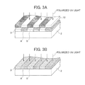
FIG. 3A and 3B are detailed diagram illustrating the exposure process. In the producing method, by irradiation of UV light (polarized UV light) having linear polarization through masks 16 blocking portions corresponding to the right-eye areas A and the left-eye areas B, the photo-alignment material film in the non-blocked left-eye areas B or right-eye areas A is aligned in the desired direction (FIG. 3A). Therefore, in the producing method, the first exposure process is performed. Subsequently, in the producing method, the entire surface is irradiated with UV light having linear polarization the direction of which is different by 90 degrees from the polarization direction in the first exposure process, and the photo-alignment material film in the right-eye areas A or the left-eye areas B which is not exposed in the first exposure process is aligned in a desired direction (FIG. 3B). Therefore, in the producing method, the right-eye areas A and the left-eye areas B are sequentially exposed through the two exposure processes, so that the alignment film 3 is formed.
FIG. 4 is a diagram illustrating equipment used for a first exposure process. In the producing method, a substrate 2 wound around a roll 17 having a large diameter is allowed to be transported, a mask 16 is disposed to face the roll 17, and irradiation of linearly polarized UV light is performed through the mask 16. In the mask 16, slits S extending in the transport direction of the substrate 2 are repetitively formed with a certain pitch in the direction perpendicular to the extension direction, and the substrate 2 is irradiated with UV light through the slits S.
In this manner, in the case where the patterned phase difference film 1 is produced by performing the consecutive processes on the elongated transparent film, it is possible to improve productivity by transporting the substrate 2 at a high speed. Therefore, it is necessary to perform the exposure process in a short time. As a method for shortening the exposure time in the exposure process, there is a method for increasing the light amount of a light source. However, in this method, it is necessary to greatly reform the light source, and in some cases, it may be difficult to perform the reforming.
On the other hand, a method for increasing the light amount irradiated on the substrate 2 by setting the slit S to have a large length may also be considered. However, as illustrated in FIG. 4, in the case of performing the exposure process while transporting the substrate 2 in the state of being wound around the roll 17, it is necessary to secure a certain degree of the distance between the substrate 2 and the mask 16, and it is not possible to maintain the light from the light source as completely parallel light in these types of facilities. Therefore, if the slit S is set to have a large length, the exposing accuracy is reduced so that it is difficult to pattern right-eye areas and left-eye areas of the patterned phase difference film 1 with high accuracy.
In addition, like this, in the case where the formation accuracy of the right-eye areas and the left-eye areas is decreased, the difference in area width between the right-eye areas and the left-eye areas is increased, so that when the patterned phase difference film 1 is installed on the liquid crystal display panel, the difference in area width is seen as a lateral stripe. In addition, if the roll 17 is set to have a large diameter, the deterioration in patterning accuracy caused in the case where the slit S is set to have a large length can be reduced. However, in this case, it is difficult to maintain the substrate 2 at an appropriate temperature due to the increase in heat capacity of the roll 17, so this method is not practical.
Therefore, in the embodiment, one slit S is formed by setting the slit S to have a large length and setting the slit S to have a width of being gradually decreased in the direction toward end portions in the longitudinal direction of the slit S. Accordingly, in the embodiment, the deterioration in accuracy is effectively prevented, and thus, the light amount irradiated on the substrate 2 is increased so that the substrate 2 is transported at a high speed.
FIG. 5 is a plan diagram illustrating the slit S formed on the mask 16. In the area range AR1 where the slit S straightly faces the roll 17 and the exposure process can be performed with sufficient accuracy, the slit S is formed according to the area width of the areas to be exposed. In addition, at the two end sides of the area range AR1, the slit S is formed so as to have a width being gradually decreased in the direction from the central portion of the slit S toward the end portions of the slit S. In the embodiment, in the portions of which the width is gradually decreased, the width is set to be decreased in a linear function so that the slit is formed in a trapezoidal shape.
Accordingly, in the embodiment, even in the case of transporting the substrate 2 at a high speed, the deterioration in accuracy is affectively prevented, and thus, the exposure process is performed with a sufficient light amount so that it is possible to simply and easily produce the patterned phase difference film with high accuracy in mass production. According to the results of various experiments, with respect to the case where the exposure process is performed in the state that the slit S is limited to the length of the area range AR1, it can be observed that in the embodiment the exposure processes can be performed with an equivalent accuracy by setting the transport speed of the substrate 2 to be double speed.
In the embodiment, in the mask used for forming an alignment film, the slits S used for the exposure process are formed to have a width being gradually decreased in the direction toward the end portions in the longitudinal direction of the slits S so that even in the case of performing the exposure process while transporting the substrate at a high speed in the state of being wound around the roll, it is possible to secure sufficient accuracy. Therefore, it is possible to simply and easily produce the patterned phase difference film at high accuracy in mass production.
[Other Embodiments]
Hereinbefore, although specific configurations suitable for embodiments of the present invention are described in detail, the configurations of the above-described embodiments of the present invention can be changed into various configurations without departing from the spirit of the present invention.
In other words, as illustrated in FIG. 6 in comparison to FIG. 5, the slit S may be formed so that each of the two ends in the longitudinal direction has a triangular shape, or so that the width is gradually changed in a curve with a quadratic function or the like instead of being changed in a linear function. In addition, as illustrated in FIG. 7, in the case where sufficient accuracy can be secured in practical use, only the one side of the slit may be set to have a gradually decreasing width.
In addition, in the above-described embodiments, the case of exposing one of the right-eye areas or the left-eye areas in the first exposure process and, after that, irradiating the entire surface with UV light in the second exposure process is described. However, the present invention is not limited thereto, but it may be widely applied to various types of exposure processes using a mask. In addition, these exposure processes include, for example, a case of exposing the entire surface in a first exposure process and partially performing alignment again by using a mask in a second exposure process, a case of performing alignment by exposing each of the right-eye areas and the left-eye areas by using a mask, and the like.
In addition, in the above-described embodiments, although the case of producing the pattern phase difference film on the assumption of the use of a liquid crystal display panel has been described, the present invention is not limited thereto. The present invention may be widely applied to cases where polarizing filters are integrally provided on the assumption of the use of an organic EL panel or a plasma display panel.

Claims (4)

The invention claimed is:
1. A method for producing a patterned phase difference film by sequentially processing an elongated transparent film material while transporting the elongated transparent film material, comprising:
forming a photo-alignment material film on the transparent film material;
forming an alignment film by performing an exposure process on the photo-alignment material film by using a mask through a photo-alignment method; and
forming a phase difference layer of a right-eye area applying phase difference corresponding to right-eye transmitting light and a left-eye area applying phase difference corresponding to left-eye transmitting light on the alignment film,
wherein the exposure process is performed by irradiation of light through the mask disposed to face a roll while transporting the transparent film material wound around the roll,
wherein the mask is formed so that slits which are used for the exposing of the photo-alignment material film a longitudinal direction of which is a direction corresponding to a longitudinal direction of the transparent film material are repetitively formed in a in a direction perpendicular to a longitudinal direction of the slit, and
wherein the slit is formed so that one end side or two end sides in the longitudinal direction of the slit has a width being gradually decreased in the direction toward end portions in the longitudinal direction of the slit.
2. The method for producing a patterned phase difference film according to claim 1, wherein the slit is formed so that a central portion in the longitudinal direction of the slit has a constant width.
3. A mask being retained so as to face a roll for transporting an elongated transparent film material and being used for exposing a photo-alignment material film formed on the transparent film material transported by the roll,
wherein slits used for the exposing of the photo-alignment material film are repetitively formed in a direction perpendicular to a longitudinal direction of the slits, and
wherein the slit is formed so that one end side or two end sides in the longitudinal direction of the slit has a width being gradually decreased in the direction toward end portions in the longitudinal direction of the slit.
4. The mask according to claim 3, wherein the slit is formed so that a central portion in the longitudinal direction of the slit has a constant width.
US14/238,996 2011-08-31 2012-08-02 Method for producing pattern phase difference film Active US8871410B2 (en)

Applications Claiming Priority (3)

Application Number Priority Date Filing Date Title
JP2011-188383 2011-08-31
JP2011188383A JP5418559B2 (en) 2011-08-31 2011-08-31 Pattern retardation film manufacturing method and mask
PCT/JP2012/069660 WO2013031467A1 (en) 2011-08-31 2012-08-02 Method for producing pattern phase difference film

Publications (2)

Publication Number Publication Date
US20140178597A1 US20140178597A1 (en) 2014-06-26
US8871410B2 true US8871410B2 (en) 2014-10-28

Family

ID=47755969

Family Applications (1)

Application Number Title Priority Date Filing Date
US14/238,996 Active US8871410B2 (en) 2011-08-31 2012-08-02 Method for producing pattern phase difference film

Country Status (6)

Country Link
US (1) US8871410B2 (en)
JP (1) JP5418559B2 (en)
KR (1) KR101445521B1 (en)
CN (1) CN103765256B (en)
TW (1) TWI429968B (en)
WO (1) WO2013031467A1 (en)

Families Citing this family (3)

* Cited by examiner, † Cited by third party
Publication number Priority date Publication date Assignee Title
WO2014156530A1 (en) * 2013-03-26 2014-10-02 富士フイルム株式会社 Laminated body manufacturing method
JP6155767B2 (en) * 2013-03-29 2017-07-05 大日本印刷株式会社 Pattern retardation film manufacturing method and pattern retardation film exposure apparatus
JP6427867B2 (en) * 2013-11-26 2018-11-28 大日本印刷株式会社 Method for producing pattern retardation film

Citations (9)

* Cited by examiner, † Cited by third party
Publication number Priority date Publication date Assignee Title
JPS6364337A (en) 1986-09-05 1988-03-22 Hitachi Ltd Semiconductor integrated circuit device
JPH01171454A (en) 1987-12-26 1989-07-06 Sanyo Kokusaku Pulp Co Ltd Mixed sweetener
JP2002098969A (en) 2000-09-26 2002-04-05 Konica Corp Method for manufacturing optical alignment layer
WO2009037889A1 (en) 2007-09-21 2009-03-26 Sharp Kabushiki Kaisha Liquid crystal display and method for manufacturing the same
US20100225864A1 (en) 2006-01-26 2010-09-09 Iichiro Inoue Production method of liquid crystal display device and liquid crystal display device
EP2372433A2 (en) 2009-02-03 2011-10-05 LG Chem, Ltd. Method for manufacturing an optical filter for a stereoscopic image display device
JP2012042530A (en) 2010-08-13 2012-03-01 Fujifilm Corp Method for manufacturing long optical film, and method for manufacturing long circularly polarizing plate
US20120212714A1 (en) * 2011-02-21 2012-08-23 Lg Display Co., Ltd. Manufacturing device of a film patterned retarder for a three dimensional display device
US20130143007A1 (en) * 2011-12-01 2013-06-06 Lg Chem, Ltd. Mask

Family Cites Families (2)

* Cited by examiner, † Cited by third party
Publication number Priority date Publication date Assignee Title
JPH064348Y2 (en) * 1988-05-16 1994-02-02 日立電線株式会社 Original photo mask
JP3925813B2 (en) * 2003-11-17 2007-06-06 シャープ株式会社 Liquid crystal display device, manufacturing method thereof, and hard mask

Patent Citations (9)

* Cited by examiner, † Cited by third party
Publication number Priority date Publication date Assignee Title
JPS6364337A (en) 1986-09-05 1988-03-22 Hitachi Ltd Semiconductor integrated circuit device
JPH01171454A (en) 1987-12-26 1989-07-06 Sanyo Kokusaku Pulp Co Ltd Mixed sweetener
JP2002098969A (en) 2000-09-26 2002-04-05 Konica Corp Method for manufacturing optical alignment layer
US20100225864A1 (en) 2006-01-26 2010-09-09 Iichiro Inoue Production method of liquid crystal display device and liquid crystal display device
WO2009037889A1 (en) 2007-09-21 2009-03-26 Sharp Kabushiki Kaisha Liquid crystal display and method for manufacturing the same
EP2372433A2 (en) 2009-02-03 2011-10-05 LG Chem, Ltd. Method for manufacturing an optical filter for a stereoscopic image display device
JP2012042530A (en) 2010-08-13 2012-03-01 Fujifilm Corp Method for manufacturing long optical film, and method for manufacturing long circularly polarizing plate
US20120212714A1 (en) * 2011-02-21 2012-08-23 Lg Display Co., Ltd. Manufacturing device of a film patterned retarder for a three dimensional display device
US20130143007A1 (en) * 2011-12-01 2013-06-06 Lg Chem, Ltd. Mask

Non-Patent Citations (1)

* Cited by examiner, † Cited by third party
Title
Aug. 27, 2013 Office Action issued in Japanese Patent Application No. 2011-188383 (with English Translation).

Also Published As

Publication number Publication date
CN103765256A (en) 2014-04-30
JP5418559B2 (en) 2014-02-19
US20140178597A1 (en) 2014-06-26
TW201323941A (en) 2013-06-16
CN103765256B (en) 2015-04-01
KR101445521B1 (en) 2014-09-29
TWI429968B (en) 2014-03-11
KR20140004243A (en) 2014-01-10
WO2013031467A1 (en) 2013-03-07
JP2013050575A (en) 2013-03-14

Similar Documents

Publication Publication Date Title
US9217925B2 (en) Method for producing pattern phase difference film, pattern phase difference film, and image display device
US8871410B2 (en) Method for producing pattern phase difference film
JP5810735B2 (en) Method for producing pattern retardation film and method for producing optical film
JP6064627B2 (en) Manufacturing method of optical film
JP6447688B2 (en) Exposure member, exposure mask holding member
JP2014219596A (en) Production method of optical film
JP2014182200A (en) Production method of optical film
JP6024240B2 (en) Method for producing pattern retardation film
JP6048187B2 (en) Pattern retardation film and image display device
JP6155767B2 (en) Pattern retardation film manufacturing method and pattern retardation film exposure apparatus
JP2013097204A (en) Metal mask for scanning exposure and scanning exposure device
JP2015049389A (en) Production method of optical film, exposure apparatus, and mask
JP6136665B2 (en) Process for producing pattern retardation film, mask, and roll body of pattern retardation film
JP6427867B2 (en) Method for producing pattern retardation film
JP6156017B2 (en) Pattern retardation film manufacturing method, exposure apparatus and mask
JP2015060148A (en) Method for manufacturing retardation film
JP2016099540A (en) Optical film, image display device, and manufacturing method of optical film
JP2015184437A (en) Production method of patterned retardation film and production method of optical film
JP2015041064A (en) Method for manufacturing patterned retardation film, and exposure apparatus
JP2015049486A (en) Production method of patterned retardation film, exposure apparatus, and mask
JP2015049418A (en) Production method of patterned retardation film, exposure apparatus, and mask
JP2016188961A (en) Production method of optical film
JP2015041065A (en) Method for manufacturing optical film
JP2012242515A (en) Manufacturing method of pattern phase difference film, and manufacturing method of metal mold for manufacturing pattern phase difference film

Legal Events

Date Code Title Description
AS Assignment

Owner name: DAI NIPPON PRINTING CO., LTD., JAPAN

Free format text: ASSIGNMENT OF ASSIGNORS INTEREST;ASSIGNORS:NISHIMURA, HIROYUKI;NAKAO, YOSHIHIDE;KAWASHIMA, TOMOYA;AND OTHERS;REEL/FRAME:032221/0208

Effective date: 20140131

STCF Information on status: patent grant

Free format text: PATENTED CASE

FEPP Fee payment procedure

Free format text: PAYOR NUMBER ASSIGNED (ORIGINAL EVENT CODE: ASPN); ENTITY STATUS OF PATENT OWNER: LARGE ENTITY

MAFP Maintenance fee payment

Free format text: PAYMENT OF MAINTENANCE FEE, 4TH YEAR, LARGE ENTITY (ORIGINAL EVENT CODE: M1551)

Year of fee payment: 4

MAFP Maintenance fee payment

Free format text: PAYMENT OF MAINTENANCE FEE, 8TH YEAR, LARGE ENTITY (ORIGINAL EVENT CODE: M1552); ENTITY STATUS OF PATENT OWNER: LARGE ENTITY

Year of fee payment: 8