US8866271B2 - Semiconductor device manufacturing method, substrate processing apparatus and semiconductor device - Google Patents
Semiconductor device manufacturing method, substrate processing apparatus and semiconductor device Download PDFInfo
- Publication number
- US8866271B2 US8866271B2 US13/250,708 US201113250708A US8866271B2 US 8866271 B2 US8866271 B2 US 8866271B2 US 201113250708 A US201113250708 A US 201113250708A US 8866271 B2 US8866271 B2 US 8866271B2
- Authority
- US
- United States
- Prior art keywords
- gas
- substrate
- wafer
- microwave
- processing chamber
- Prior art date
- Legal status (The legal status is an assumption and is not a legal conclusion. Google has not performed a legal analysis and makes no representation as to the accuracy of the status listed.)
- Active
Links
Images


Classifications
-
- H—ELECTRICITY
- H10—SEMICONDUCTOR DEVICES; ELECTRIC SOLID-STATE DEVICES NOT OTHERWISE PROVIDED FOR
- H10P—GENERIC PROCESSES OR APPARATUS FOR THE MANUFACTURE OR TREATMENT OF DEVICES COVERED BY CLASS H10
- H10P72/00—Handling or holding of wafers, substrates or devices during manufacture or treatment thereof
- H10P72/04—Apparatus for manufacture or treatment
- H10P72/0431—Apparatus for thermal treatment
- H10P72/0436—Apparatus for thermal treatment mainly by radiation
-
- H01L21/67115—
-
- H—ELECTRICITY
- H10—SEMICONDUCTOR DEVICES; ELECTRIC SOLID-STATE DEVICES NOT OTHERWISE PROVIDED FOR
- H10P—GENERIC PROCESSES OR APPARATUS FOR THE MANUFACTURE OR TREATMENT OF DEVICES COVERED BY CLASS H10
- H10P95/00—Generic processes or apparatus for manufacture or treatments not covered by the other groups of this subclass
-
- C—CHEMISTRY; METALLURGY
- C23—COATING METALLIC MATERIAL; COATING MATERIAL WITH METALLIC MATERIAL; CHEMICAL SURFACE TREATMENT; DIFFUSION TREATMENT OF METALLIC MATERIAL; COATING BY VACUUM EVAPORATION, BY SPUTTERING, BY ION IMPLANTATION OR BY CHEMICAL VAPOUR DEPOSITION, IN GENERAL; INHIBITING CORROSION OF METALLIC MATERIAL OR INCRUSTATION IN GENERAL
- C23C—COATING METALLIC MATERIAL; COATING MATERIAL WITH METALLIC MATERIAL; SURFACE TREATMENT OF METALLIC MATERIAL BY DIFFUSION INTO THE SURFACE, BY CHEMICAL CONVERSION OR SUBSTITUTION; COATING BY VACUUM EVAPORATION, BY SPUTTERING, BY ION IMPLANTATION OR BY CHEMICAL VAPOUR DEPOSITION, IN GENERAL
- C23C16/00—Chemical coating by decomposition of gaseous compounds, without leaving reaction products of surface material in the coating, i.e. chemical vapour deposition [CVD] processes
- C23C16/22—Chemical coating by decomposition of gaseous compounds, without leaving reaction products of surface material in the coating, i.e. chemical vapour deposition [CVD] processes characterised by the deposition of inorganic material, other than metallic material
- C23C16/30—Deposition of compounds, mixtures or solid solutions, e.g. borides, carbides, nitrides
- C23C16/40—Oxides
- C23C16/405—Oxides of refractory metals or yttrium
-
- C—CHEMISTRY; METALLURGY
- C23—COATING METALLIC MATERIAL; COATING MATERIAL WITH METALLIC MATERIAL; CHEMICAL SURFACE TREATMENT; DIFFUSION TREATMENT OF METALLIC MATERIAL; COATING BY VACUUM EVAPORATION, BY SPUTTERING, BY ION IMPLANTATION OR BY CHEMICAL VAPOUR DEPOSITION, IN GENERAL; INHIBITING CORROSION OF METALLIC MATERIAL OR INCRUSTATION IN GENERAL
- C23C—COATING METALLIC MATERIAL; COATING MATERIAL WITH METALLIC MATERIAL; SURFACE TREATMENT OF METALLIC MATERIAL BY DIFFUSION INTO THE SURFACE, BY CHEMICAL CONVERSION OR SUBSTITUTION; COATING BY VACUUM EVAPORATION, BY SPUTTERING, BY ION IMPLANTATION OR BY CHEMICAL VAPOUR DEPOSITION, IN GENERAL
- C23C16/00—Chemical coating by decomposition of gaseous compounds, without leaving reaction products of surface material in the coating, i.e. chemical vapour deposition [CVD] processes
- C23C16/56—After-treatment
-
- H01L21/02189—
-
- H01L21/0228—
-
- H01L21/02337—
-
- H01L21/02345—
-
- H—ELECTRICITY
- H10—SEMICONDUCTOR DEVICES; ELECTRIC SOLID-STATE DEVICES NOT OTHERWISE PROVIDED FOR
- H10P—GENERIC PROCESSES OR APPARATUS FOR THE MANUFACTURE OR TREATMENT OF DEVICES COVERED BY CLASS H10
- H10P14/00—Formation of materials, e.g. in the shape of layers or pillars
- H10P14/60—Formation of materials, e.g. in the shape of layers or pillars of insulating materials
- H10P14/63—Formation of materials, e.g. in the shape of layers or pillars of insulating materials characterised by the formation processes
- H10P14/6326—Deposition processes
- H10P14/6328—Deposition from the gas or vapour phase
- H10P14/6334—Deposition from the gas or vapour phase using decomposition or reaction of gaseous or vapour phase compounds, i.e. chemical vapour deposition
- H10P14/6339—Deposition from the gas or vapour phase using decomposition or reaction of gaseous or vapour phase compounds, i.e. chemical vapour deposition deposition by cyclic CVD, e.g. ALD, ALE or pulsed CVD
-
- H—ELECTRICITY
- H10—SEMICONDUCTOR DEVICES; ELECTRIC SOLID-STATE DEVICES NOT OTHERWISE PROVIDED FOR
- H10P—GENERIC PROCESSES OR APPARATUS FOR THE MANUFACTURE OR TREATMENT OF DEVICES COVERED BY CLASS H10
- H10P14/00—Formation of materials, e.g. in the shape of layers or pillars
- H10P14/60—Formation of materials, e.g. in the shape of layers or pillars of insulating materials
- H10P14/65—Formation of materials, e.g. in the shape of layers or pillars of insulating materials characterised by treatments performed before or after the formation of the materials
- H10P14/6516—Formation of materials, e.g. in the shape of layers or pillars of insulating materials characterised by treatments performed before or after the formation of the materials of treatments performed after formation of the materials
- H10P14/6529—Formation of materials, e.g. in the shape of layers or pillars of insulating materials characterised by treatments performed before or after the formation of the materials of treatments performed after formation of the materials by exposure to a gas or vapour
-
- H—ELECTRICITY
- H10—SEMICONDUCTOR DEVICES; ELECTRIC SOLID-STATE DEVICES NOT OTHERWISE PROVIDED FOR
- H10P—GENERIC PROCESSES OR APPARATUS FOR THE MANUFACTURE OR TREATMENT OF DEVICES COVERED BY CLASS H10
- H10P14/00—Formation of materials, e.g. in the shape of layers or pillars
- H10P14/60—Formation of materials, e.g. in the shape of layers or pillars of insulating materials
- H10P14/65—Formation of materials, e.g. in the shape of layers or pillars of insulating materials characterised by treatments performed before or after the formation of the materials
- H10P14/6516—Formation of materials, e.g. in the shape of layers or pillars of insulating materials characterised by treatments performed before or after the formation of the materials of treatments performed after formation of the materials
- H10P14/6536—Formation of materials, e.g. in the shape of layers or pillars of insulating materials characterised by treatments performed before or after the formation of the materials of treatments performed after formation of the materials by exposure to radiation, e.g. visible light
-
- H—ELECTRICITY
- H10—SEMICONDUCTOR DEVICES; ELECTRIC SOLID-STATE DEVICES NOT OTHERWISE PROVIDED FOR
- H10P—GENERIC PROCESSES OR APPARATUS FOR THE MANUFACTURE OR TREATMENT OF DEVICES COVERED BY CLASS H10
- H10P14/00—Formation of materials, e.g. in the shape of layers or pillars
- H10P14/60—Formation of materials, e.g. in the shape of layers or pillars of insulating materials
- H10P14/69—Inorganic materials
- H10P14/692—Inorganic materials composed of oxides, glassy oxides or oxide-based glasses
- H10P14/6938—Inorganic materials composed of oxides, glassy oxides or oxide-based glasses the material containing at least one metal element, e.g. metal oxides, metal oxynitrides or metal oxycarbides
- H10P14/6939—Inorganic materials composed of oxides, glassy oxides or oxide-based glasses the material containing at least one metal element, e.g. metal oxides, metal oxynitrides or metal oxycarbides characterised by the metal
- H10P14/69395—Inorganic materials composed of oxides, glassy oxides or oxide-based glasses the material containing at least one metal element, e.g. metal oxides, metal oxynitrides or metal oxycarbides characterised by the metal the material containing zirconium, e.g. ZrO2
-
- H—ELECTRICITY
- H10—SEMICONDUCTOR DEVICES; ELECTRIC SOLID-STATE DEVICES NOT OTHERWISE PROVIDED FOR
- H10P—GENERIC PROCESSES OR APPARATUS FOR THE MANUFACTURE OR TREATMENT OF DEVICES COVERED BY CLASS H10
- H10P34/00—Irradiation with electromagnetic or particle radiation of wafers, substrates or parts of devices
- H10P34/40—Irradiation with electromagnetic or particle radiation of wafers, substrates or parts of devices with high-energy radiation
- H10P34/42—Irradiation with electromagnetic or particle radiation of wafers, substrates or parts of devices with high-energy radiation with electromagnetic radiation, e.g. laser annealing
-
- H—ELECTRICITY
- H10—SEMICONDUCTOR DEVICES; ELECTRIC SOLID-STATE DEVICES NOT OTHERWISE PROVIDED FOR
- H10P—GENERIC PROCESSES OR APPARATUS FOR THE MANUFACTURE OR TREATMENT OF DEVICES COVERED BY CLASS H10
- H10P95/00—Generic processes or apparatus for manufacture or treatments not covered by the other groups of this subclass
- H10P95/90—Thermal treatments, e.g. annealing or sintering
-
- H01L28/40—
-
- H—ELECTRICITY
- H10—SEMICONDUCTOR DEVICES; ELECTRIC SOLID-STATE DEVICES NOT OTHERWISE PROVIDED FOR
- H10D—INORGANIC ELECTRIC SEMICONDUCTOR DEVICES
- H10D1/00—Resistors, capacitors or inductors
- H10D1/60—Capacitors
- H10D1/68—Capacitors having no potential barriers
Definitions
- the present disclosure relates to a substrate processing technology for manufacturing a semiconductor device, such as an integrated circuit (IC), on a substrate, and more particularly relates to a semiconductor manufacturing apparatus for manufacturing a semiconductor device by processing a substrate such as a semiconductor wafer (hereinafter, referred to as a wafer), a substrate processing apparatus for processing a substrate, or a semiconductor device manufacturing method.
- a substrate processing technology for manufacturing a semiconductor device, such as an integrated circuit (IC)
- a substrate such as a semiconductor wafer (hereinafter, referred to as a wafer)
- a substrate processing apparatus for processing a substrate or a semiconductor device manufacturing method.
- PVD Physical Vapor Deposition
- CVD Chemical Vapor Deposition
- ALD Atomic Layer Deposition
- a PVD method refers to a method that forms a film of elements contained in a raw material on a substrate by using raw material atoms physically released in gas phase from a solid raw material by ion bombardment or heat energy.
- a CVD method refers to a method that forms a film of atoms contained in raw-material molecules by using the reaction of two or more kinds of raw materials in gas phase or on a substrate surface. Since the CVD method uses the reaction in gas phase or on the substrate surface, it has excellent step coverage as compared to the PVD method.
- the ALD method refers to a method that alternately supplies two or more kinds of raw materials, which are used for film formation, to a substrate one by one under a certain film forming condition (temperature or time) to adsorb the raw materials on the substrate in units of atomic layer, and forms a film through an atomic-layer-level control by using a surface reaction.
- the ALD method can be performed at a lower substrate temperature (processing temperature) than the CVD method and can control film thickness according to the number of film forming cycles.
- an insulating layer formed on a substrate for example, there may be oxide and nitride of hafnium (Hf), zirconium (Zr) or aluminum (Al), which are high-k (high dielectric constant) films having a high relative dielectric constant.
- a hafnium oxide film (HfO x ), a zirconium oxide film (ZrO x ), and the like, which are high-k films are formed by reacting an organic or inorganic material containing Hf or Zr with an oxidized gas such as oxygen (O 2 ) or ozone (O 3 ).
- a capacitor electrode of a capacitor of a Dynamic Random Access Memory (DRAM) or a transistor gate structure has a laminated structure in which an insulating film is interposed between electrodes.
- a capacitor is formed to have a laminated structure in which the high-k film as a capacitive insulating film is interposed between the titanium nitride films being top and bottom electrodes.
- the titanium nitride film is formed using a Ti-containing gas such as titanium tetrachloride (TiCl 4 ) and a nitriding agent (nitrogen(N)-containing gas) such as ammonia (NH 3 ).
- a zirconium oxide film is formed using an oxidizing agent (oxygen(O)-containing gas) such as tetrakis(ethylmethylamino)zirconium (TEMAZ:Zr[N(CH 3 )CH 2 CH 3 ] 4 ) and ozone (O 3 ).
- crystallization annealing may be carried out in order to improve the relative dielectric constant. This is because the relative dielectric constant of the high-k film is dependent on the crystal structure thereof.
- a high-k film is formed on a bottom electrode being made of a titanium nitride film. Due to poor oxidizing ability of an oxidizing agent, instability of process conditions, or requirement for low temperature, all raw materials constituting the high-k film cannot be completely oxidized, and oxygen is liberated when crystallization annealing is carried out in order to improve the relative dielectric constant of the high-k film. For these reasons, defects may occur in the film. For example, oxygen may be lost in the high-k film or carbon (C) may remain in the high-k film. Since these film defects serve as a path through which an electric current flows, phenomenon causing defects such as an increase in leakage current of the capacitor or degradation of the capacitor may occur.
- the present disclosure provides some embodiments of a semiconductor device manufacturing method, a substrate processing apparatus, and a semiconductor device, which can achieve optimization of crystal structure, acceleration of crystallization, reduction of oxygen defect, and reduction of residual impurity, during a manufacturing process of a semiconductor device with a high-k film, and can perform a reforming process suitable for an insulating film.
- a semiconductor device manufacturing method including: loading a substrate, on which a high-k film is formed, into a processing chamber; heating the high-k film through irradiation of a microwave on the substrate; and unloading the substrate from the processing chamber.
- a substrate processing apparatus including: a processing chamber; a microwave generating device configured to generate a microwave; a waveguide configured to supply the microwave generated in the microwave generating device to the processing chamber, and a control unit configured to control the microwave generating device to supply the microwave from the waveguide to the processing chamber accommodating a substrate on which a high-k film is formed.
- a substrate processing apparatus including: a reaction vessel configured to accommodate a plurality of substrates on which a high-k film is formed; a substrate support member configured to support the substrates stacked within the reaction vessel; a microwave generating device configured to generate a microwave; and a waveguide configured to supply the microwave generated in the microwave generating device to the reaction vessel, wherein the substrates are stacked in the substrate support member such that a space having a height of more than half a wavelength of the microwave supplied into the reaction vessel is formed on the top surface of the respective substrates, and the waveguide is installed on a sidewall of the reaction vessel.
- FIG. 1 is a perspective view of a film forming processing apparatus according to a first embodiment of the present disclosure.
- FIG. 2 is a schematic view of a processing furnace and a peripheral structure thereof according to the first embodiment of the present disclosure.
- FIG. 3 is a cross-sectional view taken along line A-A of FIG. 2 .
- FIG. 4 is a vertical sectional view of a reforming processing apparatus according to the first embodiment of the present disclosure.
- FIG. 5 is a diagram illustrating an example of a correlation between a microwave power and a substrate temperature.
- FIG. 6 is a flowchart of a film forming operation of the film forming processing apparatus according to the first embodiment of the present disclosure.
- FIG. 7 is a diagram illustrating gas supply timing in a film forming operation.
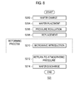
- FIG. 8 is a flowchart of a reforming operation of the reforming processing apparatus according to the first embodiment of the present disclosure.
- FIG. 9 is a vertical sectional view of a reforming processing apparatus according to a second embodiment of the present disclosure.
- FIG. 10 is a vertical sectional view of a reforming processing apparatus according to a third embodiment of the present disclosure.
- FIG. 11A , FIG. 11B and FIG. 11C are schematic views explaining another example of the reforming processing apparatus according to the third embodiment of the present disclosure.
- FIG. 12A , FIG. 12B and FIG. 12C are schematic views explaining an example of a reforming processing apparatus according to a fourth embodiment of the present disclosure.
- FIG. 13 is a schematic view explaining an example of a reforming processing apparatus according to a fifth embodiment of the present disclosure.
- FIG. 14 is a flowchart of a reforming operation of the reforming processing apparatus according to the fifth embodiment of the present disclosure.
- FIG. 15 is a schematic view explaining another example of the reforming processing apparatus according to the fifth embodiment of the present disclosure.
- FIG. 16 is a schematic view explaining another example of the reforming processing apparatus according to the fifth embodiment of the present disclosure.
- FIG. 17 is a schematic view explaining another example of the reforming processing apparatus according to the fifth embodiment of the present disclosure.
- FIG. 18 is a schematic view explaining another embodiment of a reforming processing apparatus according to a sixth embodiment of the present disclosure.
- FIG. 19 is a flowchart of a reforming operation of the reforming processing apparatus according to a seventh embodiment of the present disclosure.
- a substrate processing apparatus system is a semiconductor manufacturing apparatus system that performs a substrate processing process, for example, a film forming process and a reforming process in a method for manufacturing a semiconductor device (Integrated Circuit (IC))
- IC Integrated Circuit
- the substrate processing apparatus system includes a film forming processing apparatus 10 and a reforming processing apparatus 200 .
- FIG. 1 is a perspective view of a film forming processing apparatus 10 according to an embodiment of the present disclosure. Also, in the following description, a case where a batch type vertical apparatus is used as the film forming processing apparatus 10 will be described.
- a cassette 4 is used as a wafer carrier that accommodates a wafer 2 which is a substrate made of silicon or the like.
- the film forming processing apparatus 10 includes a housing 12 . At a lower part of a front wall 12 a of the housing 12 , a front maintenance opening 18 is formed to allow maintenance. At the front maintenance opening 18 , an openable/closable front maintenance door 20 is installed.
- a cassette loading/unloading opening 22 is formed to communicate with the interior and exterior of the housing 12 .
- the cassette loading/unloading opening 22 is configured to be opened or closed by a front shutter 24 .
- a cassette stage 26 is installed inside the housing 12 facing the cassette loading/unloading opening 22 .
- the cassette 4 is carried in onto the cassette stage 26 or is carried out from the cassette stage 26 by an in-plant carrying device (not shown).
- the cassette 4 is loaded onto the cassette stage 26 by means of the in-plant carrying device.
- the wafer 2 is held in a vertical position inside the cassette 4 , and a wafer charging/discharging opening of the cassette 4 faces upward.
- the cassette stage 26 is configured so that the cassette 4 is turned to the right toward the rear of the housing 12 and rotated 90 degrees clockwise, whereby the wafer 2 within the cassette 4 is set in a horizontal position and the wafer charging/discharging opening of the cassette 4 faces toward the rear of the housing 12 .
- a cassette shelf 28 is installed at an approximately center lower part of the inside of the housing 12 in a front and rear direction.
- the cassette shelf 28 is configured such that a plurality of cassettes 4 are stored in multiple stages and in multiple rows.
- a transfer shelf 30 accommodates the cassettes 4 that are transfer targets of a wafer transfer mechanism 36 to be described later.
- a preliminary cassette shelf 32 can store preliminary cassettes 4 .
- a cassette carrier device 34 is located between the cassette stage 26 and the cassette shelf 28 .
- the cassette carrier device 34 includes a cassette elevator 34 a , which holds and elevates the cassettes 4 , and a cassette carrying mechanism 34 b as a carrying mechanism.
- the cassette carrier device 34 carries the cassettes 4 among the cassette stage 26 , the cassette shelf 28 , and the preliminary cassette shelf 32 through the operation of the cassette elevator 34 a and the cassette carrier device 34 b.
- the wafer transfer mechanism 36 includes a wafer transfer device 36 a , which can rotate the wafer 2 in a horizontal direction or move the wafer 2 straight, and a wafer transfer device elevator 36 b , which elevates the wafer transfer device 36 a.
- the wafer transfer device elevator 36 b is installed at a right end of the housing 12 .
- the wafer transfer mechanism 36 picks up the wafer 2 , charges the wafer 2 into a boat 38 and discharges the wafer 2 from the boat 38 with tweezers 36 c of the wafer transfer device 36 a through operation of the wafer transfer device 36 a and the wafer transfer device elevator 36 b.
- a processing furnace 40 is installed at the rear upper part of the housing 12 .
- a lower end of the process furnace 40 is configured to be opened or closed by a furnace throat shutter 42 .
- a boat elevator 44 is installed below the processing furnace 40 to elevate the boat 38 to the processing furnace 40 .
- An arm 46 as a connecting tool is connected to the boat elevator 44 , and a seal cap 48 as a lid is horizontally installed on the arm 46 .
- the boat 38 has a plurality of holding members to horizontally hold a plurality of wafers 2 (for example, about 50 to 150 wafers) with their centers being aligned vertically.
- the seal cap 48 is made of a metal, for example, a stainless steel, and is formed in a disk shape.
- the seal cap 48 vertically supports the boat 38 and is configured to close the lower end of the processing furnace 40 .
- a first clean unit 50 a is installed to supply clean air, which is a cleaned atmosphere.
- the first clean unit 50 a is provided with a supply fan and a dust-proof filter, so that clean air is circulated to the inside of the housing 12 .
- a second clean unit 50 b is installed to supply clean air.
- the second clean unit 50 b also is provided with a supply fan and a dust-proof filter, like the first clean unit 50 a . Clean air supplied from the second clean unit 50 b is circulated to the vicinity of the wafer transfer device 36 a , the boat 38 , and the like, and then, is exhausted from an exhaust device (not shown) to the exterior of the housing 12 .
- the cassette loading/unloading opening 22 Prior to supplying the cassette 4 to the cassette stage 26 , the cassette loading/unloading opening 22 is opened by the front shutter 24 . Thereafter, the cassette 4 is loaded onto the cassette stage 26 through the cassette loading/unloading opening 22 . At this time, the wafer 2 inside the cassette 4 is placed in a vertical position, and the wafer charging/discharging opening of the cassette 4 faces upward.
- the cassette 4 is turned to the right and rotated at 90 degrees clockwise by the cassette stage 26 , so that the wafer 2 within the cassette 4 is set in a horizontal position and the wafer charging/discharging opening of the cassette 4 faces toward the rear of the housing 12 .
- the cassette 4 is automatically transferred to a designated shelf position of the cassette shelf 28 or the preliminary cassette shelf 32 by the cassette transfer device 34 to be temporarily stored therein, and is transferred from the cassette shelf 28 or the preliminary cassette shelf 32 to the transfer shelf 30 by the cassette transfer device 34 , or is directly transferred to the transfer shelf 30 .
- the wafer 2 is picked up from the cassette 4 through the wafer charging/discharging opening by the tweezers 36 c of the wafer transfer device 36 a , and is charged into the boat 38 .
- the wafer transfer device 36 a which transfers the wafer 2 to the boat 38 , is returned to the cassette 4 and charges a next wafer 2 into the boat 38 .
- the furnace throat shutter 42 is opened and the lower end part of the process furnace 40 is opened. Subsequently, the boat 38 holding a wafer 2 group is loaded into the processing furnace 40 by elevating the seal cap 48 by the boat elevator 44 .
- the wafer 2 is processed in the processing furnace 40 . After processing, the cassette 4 and the wafer 2 are discharged outside the housing 12 in a reverse procedure to the above-described procedure.
- FIG. 2 is a schematic view of the processing furnace 40 and its peripheral structure.
- FIG. 3 is a sectional view taken along line A-A of FIG. 2 .
- the processing furnace 40 includes a heater 72 as a heating unit (heating mechanism).
- the heater 72 has a cylindrical shape and is vertically installed by being supported by a heater base (not shown) as a holding plate.
- a reaction tube 74 constituting a reaction vessel (processing vessel) is installed concentrically with the heater 72 .
- a seal cap 48 which can air-tightly close a lower end opening of the reaction tube 74 .
- the seal cap 48 contacts the lower end part of the reaction tube 74 .
- an O-ring 76 is installed as a seal member that contacts the lower end part of the reaction tube 74 .
- a processing chamber 80 is formed in the processing furnace 40 .
- the processing chamber 80 performs a film formation process with at least the reaction tube 74 and the seal cap 48 .
- a rotating mechanism 82 rotates the boat 38 located at an opposite side of the processing chamber as seal cap 48 .
- a rotating shaft 84 of the rotating mechanism 82 passes through the seal cap 48 to be connected to the boat 38 , and rotates the wafer 2 by rotating the boat 38 .
- the boat 38 is loaded into or unloaded from the processing chamber 80 .
- the boat 38 is erected on the seal cap 48 via a quartz cap 86 as a heat insulating member.
- the quartz cap 86 is made of a heat resistant material, for example, quartz or silicon carbide, and functions as a heat insulating unit and simultaneously as a holding body to hold the boat 38 .
- an exhaust pipe 90 is installed to exhaust atmosphere within the processing chamber 80 .
- a vacuum pump 96 as a vacuum exhaust device is connected to the exhaust pipe 90 .
- a pressure sensor 92 which is a pressure detector (pressure detecting unit) to detect pressure inside the processing chamber 80
- APC Auto Pressure Controller
- the vacuum pump 96 performs a vacuum exhaust such that pressure inside the processing chamber 80 is set to a predetermined pressure (vacuum degree).
- the APC valve 94 is an on-off valve that can start or stop the vacuum exhaust inside the processing chamber 80 by opening or closing a valve, and also adjust the pressure by adjusting a valve opening degree.
- an exhaust system is configured by the exhaust pipe 90 , the pressure sensor 92 , the APC valve 94 , and the vacuum pump 96 .
- a temperature sensor 98 is installed as a temperature detector.
- the temperature inside the processing chamber 80 is maintained at a desired temperature distribution by adjusting an on/off state of the heater 72 , based on temperature information detected by the temperature sensor 98 .
- the temperature sensor 98 is formed in an L shape and is installed along the inner wall of the reaction tube 74 .
- nozzles 100 a , 100 b , 100 c and 100 d are installed to pass through the reaction tube 74 at the lower part thereof.
- Gas supply pipes 102 a , 102 b , 102 c and 102 d are connected to the nozzles 100 a , 100 b , 100 c and 100 d , respectively.
- the four nozzles 100 a to 100 d and the four gas supply pipes 102 a to 102 d are installed in the reaction tube 74 , and the processing chamber 80 is configured to supply a plurality of gases to the inside of the reaction tube 74 .
- a mass flow controller (MFC) 104 a that functions as a flow rate controller (flow rate control unit), a vaporizer 106 that functions as a vaporizing device (vaporizing unit) to vaporize liquid raw material and generate a vaporized gas as a raw material gas, and a valve 108 a that functions as an on-off valve are installed in this order from an upstream direction.
- MFC mass flow controller
- valve 108 a By opening the valve 108 a , the vaporized gas generated within the vaporizer 106 a is supplied into the processing chamber 80 via the nozzle 100 a.
- a bent line 110 a connected to the exhaust pipe 90 is connected between the vaporizer 106 a of the gas supply pipe 102 a and the valve 108 a .
- a valve 118 a being an on-off valve is installed in the bent line 110 a . If the raw material gas is not supplied to the processing chamber 80 , the raw material gas may be supplied to the bent line 110 a via the valve 118 a.
- the supply of the vaporized gas into the processing chamber 80 can be stopped while continuing the generation of the vaporized gas in the vaporizer 106 a.
- a predetermined time is required to stably generate the vaporized gas, but, in the current embodiment, it is possible to switch between the supply and non-supply of the vaporized gas into the processing chamber 80 in a short time by the switching operation of the valve 108 a and the valve 118 a.
- an inert gas supply pipe 122 a is connected to a downstream side of the valve 108 a (a side close to the reaction tube 74 ).
- an MFC 124 a and a valve 128 a being an on-off valve are installed in this order from an upstream direction.
- the nozzle 100 a is connected to a front end of the gas supply pipe 102 a .
- the nozzle 100 a is installed in an arc-shaped space between the inner wall of the reaction tube 74 and the wafer 2 to extend in an upward stacking direction of the wafer 2 along the inner wall of the reaction tube 74 .
- the nozzle 100 a is configured with an L-shaped long nozzle. At the side of the nozzle 100 a , a plurality of gas supply holes 130 a through which gas is supplied are formed. The gas supply holes 130 a are opened toward the center of the reaction tube 74 .
- the gas supply holes 130 a are formed from the lower part to the upper part of the reaction tube 74 .
- the openings of respective gas supply holes 130 a have the same area and also are provided at the same opening pitch.
- a first gas supply system is configured by the gas supply pipe 102 a , the bent line 110 a , the MFC 104 a , the vaporizer 106 a , the valves 108 a and 118 a , and the nozzle 100 a.
- a first inert gas supply system is configured by the inert gas supply pipe 122 a , the MFC 124 a , and the valve 128 a.
- an MFC 104 b and a valve 108 b being an on-off valve are installed in this order from an upstream direction.
- an inert gas supply pipe 122 b is connected to a downstream side of the valve 108 b (a side close to the reaction tube 74 ).
- an MFC 124 b and a valve 128 b being an on-off valve are installed in this order from an upstream direction.
- the nozzle 100 b is connected to a front end of the gas supply pipe 102 b .
- the nozzle 100 b is installed in an arc-shaped space between the inner wall of the reaction tube 74 and the wafer 2 to extend in an upward stacked direction of the wafer 2 along the inner wall of the reaction tube 74 in.
- the nozzle 100 b is configured with an L-shaped long nozzle. At the side of the nozzle 100 b , a plurality of gas supply holes 130 b through which gas is supplied are formed, and the gas supply holes 130 b are opened toward the center of the reaction tube 74 .
- the gas supply holes 130 b are formed from the lower part to the upper part of the reaction tube 74 .
- the openings of respective gas supply holes 130 b have the same area and also are provided at the same opening pitch.
- a second gas supply system is configured by the gas supply pipe 102 b , the MFC 104 b , the valve 108 b , and the nozzle 100 b.
- a second inert gas supply system is configured by the inert gas supply pipe 122 b , the MFC 124 b , and the valve 128 b.
- an MFC 104 c a vaporizer 106 c , and a valve 108 c being an on-off valve are installed in this order from an upstream direction.
- valve 108 c By opening the valve 108 c , the vaporized gas generated within the vaporizer 106 c is supplied into the processing chamber 80 via the nozzle 100 c.
- a bent line 110 c connected to the exhaust pipe 90 is connected between the vaporizer 106 c of the gas supply pipe 102 c and the valve 108 c .
- a valve 118 c being an on-off valve is installed in the bent line 110 c . If the raw material gas is not supplied to the processing chamber 80 , the raw material gas may be supplied to the bent line 110 c via the valve 118 c.
- the supply of the vaporized gas into the processing chamber 80 can be stopped while continuing the generation of the vaporized gas in the vaporizer 106 c.
- a predetermined time is required in some embodiments to stably generate the vaporized gas, but, in the current embodiment, it is possible to switch between the supply and non-supply of the vaporized gas into the processing chamber 80 in a short time by the switching operation of the valve 108 a and the valve 118 a.
- an inert gas supply pipe 122 c is connected to a downstream side of the valve 108 c .
- an MFC 124 c and a valve 128 c being an on-off valve are installed in this order from an upstream direction.
- the nozzle 100 c is connected to a front end of the gas supply pipe 102 c .
- the nozzle 100 c is installed in an arc-shaped space between the inner wall of the reaction tube 74 and the wafer 2 to extend in an upward stacked direction of the wafer 2 along the inner wall of the reaction tube 74 .
- the nozzle 100 c is configured with an L-shaped long nozzle. At the side of the nozzle 100 c , a plurality of gas supply holes 130 c through which gas is supplied are formed, and the gas supply holes 130 c are opened toward the center of the reaction tube 74 .
- the gas supply holes 130 c are formed from the lower part to the upper part of the reaction tube 74 .
- the openings of respective gas supply holes 130 c have the same area and also are provided at the same opening pitch.
- a third gas supply system is configured by the gas supply pipe 102 c , the bent line 110 c , the MFC 104 c , the vaporizer 106 c , the valves 108 c and 118 c , and the nozzle 100 c.
- a third inert gas supply system is configured by the inert gas supply pipe 122 c , the MFC 124 c , and the valve 128 c.
- an ozonizer 132 being an ozone (O 3 ) gas generating apparatus
- a valve 134 d an MFC 104 d
- a vaporizer 106 d a vaporizer 106 d
- a valve 108 d being an on-off valve
- An upstream side of the gas supply pipe 102 d is connected to an oxygen gas supply source (not shown) that supplies oxygen (O 2 ) gas.
- O 2 gas supplied to the ozonizer 132 is changed to O 3 gas in the ozonizer, and the O 3 gas is supplied into the processing chamber 80 .
- a bent line 110 d connected to the exhaust pipe 90 is connected between the ozonizer 132 of the gas supply pipe 102 d and the valve 134 d .
- a valve 118 d being an on-off valve is installed at the bent line 110 d . If O 3 gas is not supplied into the processing chamber 80 , O 3 gas may be supplied to the bent line 110 d via the valve 118 d.
- a predetermined time is required in some embodiments to stably generate O 3 gas, but, in the current embodiment, it is possible to switch between the supply and non-supply of the O 3 gas into the processing chamber 80 in a short time by the switching operation of the valve 108 d , the valve 134 d , and the valve 118 d.
- an inert gas supply pipe 122 d is connected to a downstream side of the valve 108 d .
- an MFC 124 d and a valve 128 d being an on-off valve are installed in this order from an upstream direction.
- the nozzle 100 d is connected to a front end of the gas supply pipe 102 d .
- the nozzle 100 d is installed in an arc-shaped space between the inner wall of the reaction tube 74 and the wafer 2 to extend in an upward stacked direction of the wafer 2 along the inner wall of the reaction tube 74 .
- the nozzle 100 d is configured with an L-shaped long nozzle. At the side of the nozzle 100 d , a plurality of gas supply holes 130 d through which gas is supplied are formed, and the gas supply holes 130 d are opened toward the center of the reaction tube 74 .
- the gas supply holes 130 d are formed from the lower part to the upper part of the reaction tube 74 .
- the openings of respective gas supply holes 130 d have the same area and also are provided at the same opening pitch.
- a fourth gas supply system is configured by the gas supply pipe 102 d , the bent line 110 d , the MFC 104 d , the ozonizer 132 , the valves 108 d , 134 d and 118 d , and the nozzle 100 d.
- a fourth inert gas supply system is configured by the inert gas supply pipe 122 d , the MFC 124 d , and the valve 128 d.
- a titanium raw material gas i.e., a titanium (Ti) containing gas (titanium containing gas), as an example of a first raw material gas (processing gas) is supplied into the processing chamber 80 via the MFC 104 a , the vaporizer 106 a , the valve 108 a , and the nozzle 100 a.
- titanium tetrachloride TiCl 4
- TiCl 4 titanium tetrachloride
- the first raw material gas may be any one of solid, liquid, and gas at ordinary temperature and pressure. However, in the current embodiment, the case where the first raw material is a liquid will be described. In the case where the first raw material is a gas at an ordinary temperature and pressure, the vaporizer 106 a may be omitted.
- a nitrogen (N) containing processing gas nitrogen containing gas
- nitrogen containing gas nitrogen containing gas
- a nitriding gas nitriding agent
- nitrogen containing gas ammonia (NH 3 ) gas, nitrogen (N 2 ) gas, nitrogen trifluoride (NF 3 ), or N 3 H 8 gas may be used.
- zirconium raw material gas i.e., zirconium (Zr) containing gas (zirconium containing gas) as the second raw material gas (processing gas) is supplied into the processing chamber 80 via the MFC 104 c , the vaporizer 106 c , the valve 108 c , and the nozzle 100 c.
- tetrakis(ethylmethylamino)zirconium (TEMAZ:Zr(N(CH 3 )C 2 H 5 ) 4 may be used.
- the second raw material gas may be any one of solid, liquid, and gas at ordinary temperature and pressure. However, in the current embodiment, the case where the second raw material is the liquid will be described. In the case where the second raw material is the gas at an ordinary temperature and pressure, the vaporizer 106 c may be omitted.
- O 3 gas as an oxidizing gas is supplied into the processing chamber 80 via the valve 134 d , the MFC 104 d , and the valve 108 d .
- O 3 gas is generated by supplying oxygen (O) containing processing gas (oxygen containing gas) to the ozonizer 132 .
- the oxygen containing gas may use O 2 gas.
- O 2 gas as the oxidizing gas can be supplied into the processing chamber 80 , without generating O 3 gas in the ozonizer 132 .
- nitrogen (N 2 ) gas as an inert gas is supplied into the processing chamber 80 via the corresponding MFC 124 a to 124 d , valves 128 a to 128 d , gas supply pipes 102 a to 102 d , and the nozzles 100 a to 100 d.
- a noble gas such as argon (Ar) gas, helium (He) gas, neon (Ne) gas, and xenon (Xe) gas may be used as the inert gas.
- FIG. 4 is a vertical sectional view of the reforming processing apparatus 200 according to an embodiment of the present disclosure.
- the reforming processing apparatus 200 includes a processing chamber (reforming chamber) 210 , a transfer chamber (not shown), and a microwave supply unit (microwave generating apparatus, a microwave generator).
- the processing chamber 210 reforms the wafer 2 .
- the microwave supply unit includes a microwave generating unit 220 , a waveguide 221 , and a waveguide opening 222 .
- the microwave generating unit 220 generates, for example, a fixed frequency microwave or a variable frequency microwave.
- the microwave generating unit 220 uses, for example, a magnetron, a klystron, or a gyrotron.
- the microwave generated in the microwave generating unit 220 is introduced into the processing chamber 210 from the waveguide opening 222 communicating with the processing chamber 210 via the wave guide 221 .
- the microwave is introduced horizontally to the wafer 2 from a lateral direction, it is not limited thereto.
- the microwave may be introduced from the upper part of the processing chamber 210 in a vertical direction with respect to the wafer 2 .
- there may be a plurality of waveguides 221 and the microwave may be introduced from the plurality of waveguides 221 to the processing chamber 210 .
- the microwave introduced into the processing chamber 210 is repeatedly reflected off the walls of the processing chamber 210 .
- the microwave is reflected in various directions within the processing chamber 210 , so the inside of the processing chamber 210 is filled with the microwaves.
- the microwave contacting the wafer 2 within the processing chamber 210 is absorbed into the wafer 2 , and the wafer 2 is dielectric-heated by the microwave.
- the microwave is a generic term for electromagnetic waves having a frequency band of about 300 MHz to about 300 GHz.
- the microwave is an electromagnetic wave having a wavelength of about 1 m to about 1 mm.
- This microwave includes a millimeter wave of about 30 GHz to about 300 GHz.
- FIG. 5 illustrates correlation data of the microwave power and the wafer temperature when a microwave is irradiated on a silicon wafer.
- FIG. 5 is a diagram illustrating an example of the correlation of the microwave power and the wafer temperature. As illustrated in FIG. 5 , the wafer temperature rises as the microwave power increases.
- the wafer temperature changes depending on the size or shape of the processing chamber, the position of the waveguide of the microwave, and the position of the wafer.
- the wafer temperature value of the data herein is exemplary. However, the correlation that the wafer temperature increases as the microwave power increases is unchanging.
- the processing vessel 218 forming the processing chamber 210 is made of, for example, a metallic material such as aluminum (Al) and stainless steel (SUS), and the processing chamber 210 is microwave-shielded from the exterior.
- a substrate support pin 213 is installed as a substrate support unit that supports the wafer 2 .
- the substrate support pin 213 is installed such that the center of the supported wafer 2 and the center of the processing chamber 210 are approximately aligned with each other in a vertical direction.
- the substrate support pin 213 is configured with a plurality of support pins (in the current embodiment, three support pins) composed of, for example, quartz or Teflon (trademark), and the upper end part thereof supports the wafer 2 .
- a conductive substrate support table (substrate holding table) 212 being a substrate temperature control unit (including a temperature control mechanism) is installed below the wafer 2 .
- the substrate support table 212 is made of, for example, a metallic material being a conductor such as aluminum (Al) or the like.
- the substrate support table 212 has a circular shape whose outer diameter is larger than that of the wafer 2 , when viewed from above the top surface, and is formed in a disk shape or a cylindrical shape.
- the substrate support table 212 is made of a metallic material, the potential of the microwave becomes zero in the substrate support table 212 . Therefore, if the wafer 2 is directly placed on the surface of the substrate support table 212 , the electric field intensity of the microwave becomes weak. Therefore, in the current embodiment, the wafer 2 is placed at a position of quarter wavelength ( ⁇ /4) of the microwave from the substrate support table 212 , or a position of an odd multiple of ⁇ /4. Since the electric field is strong at the position of the odd multiple of ⁇ /4, the wafer 2 can be efficiently heated by the microwave.
- the wavelength of the microwave is 51.7 mm
- the height from the substrate support table 212 to the wafer 2 is set to 12.9 mm.
- a coolant passage 231 through which coolant flows so as to cool the wafer 2 is formed.
- water is used as the coolant, and other coolant such as a cooling chiller may also be used.
- the coolant passage 231 is connected to a coolant supply pipe 232 , which supplies the coolant from the exterior of the processing chamber 210 to the coolant passage 231 , and a coolant discharge pipe 236 , which discharges the coolant from the coolant passage 231 .
- an on-off valve 233 opening/closing the coolant supply pipe 232 , a flow rate control device 234 controlling a coolant flow rate, and a coolant source 35 are installed in this order from a downstream.
- the on-off valve 233 and the flow rate control device 234 are electrically connected to a controller 300 to be described later, and are controlled by the controller 300 .
- a temperature detector 214 detecting the temperature of the wafer 2 and a temperature control mechanism (not shown) are installed in the processing chamber 210 .
- the temperature detector 214 may use, for example, an infrared sensor.
- the temperature detector 214 is electrically connected to the controller 300 . If the temperature of the wafer 2 detected by the temperature detector 214 is higher than a predetermined temperature, the controller 300 adjusts a flow rate of the cooling water flowing through the coolant passage 231 by controlling the on-off valve 233 and the flow rate control device 234 so that the temperature of the wafer 2 becomes the predetermined temperature. On the contrary, if the temperature of the wafer 2 is lower than the predetermined temperature, the wafer 2 may be heated by the temperature control mechanism so as to improve the effect of the reforming processing.
- a gas supply pipe 252 through which nitrogen (N 2 ) gas or the like is introduced is installed at the top wall of the processing chamber 210 .
- a gas supply source 255 a gas supply source 255 , a flow rate control device 254 adjusting a gas flow rate, and a valve 253 opening/closing a gas passage are installed in this order from an upstream.
- a valve 253 opening/closing a gas passage is installed in this order from an upstream.
- gas is introduced from the gas supply pipe 252 into the processing chamber 210 or the introduction of gas is stopped.
- the gas introduced from the gas supply pipe 252 is used to cool the wafer 2 or is used as a purge gas to extrude gas inside the processing chamber 210 .
- a diffuser for diffusing gas uniformly may be installed.
- a gas supply unit is configured by the gas supply source 255 , the gas supply pipe 252 , the flow rate control device 254 , and the valve 253 .
- the flow rate control device 254 and the valve 253 are electrically connected to the controller 300 and are controlled by the controller 300 .
- a gas exhaust pipe 262 is installed at the sidewall of the processing chamber 210 to exhaust gas inside the processing chamber 210 .
- a pressure regulating valve 263 and a vacuum pump 264 being an exhaust device are installed in this order from an upstream, and the pressure inside the processing chamber 210 is regulated to a predetermined value by adjusting the opening degree of the pressure regulating valve 263 .
- a gas exhaust unit is configured by the gas exhaust pipe 262 , the pressure regulating valve 263 , and the vacuum pump 264 .
- the pressure regulating valve 263 and the vacuum pump 264 are electrically connected to the controller 300 and the pressure regulation is controlled by the controller 300 .
- a wafer transfer opening 271 through which the wafer 2 is transferred to the inside and outside of the processing chamber 210 is installed.
- a gate valve 272 is installed at the wafer transfer opening 271 .
- the gate valve 272 is opened by a gate valve driving unit 273 , the inside of the processing chamber 210 and the inside of the transfer chamber communicate with each other.
- a transfer robot (not shown) for transferring the wafer 2 is installed.
- a transfer arm is provided to support the wafer 2 when the wafer 2 is transferred.
- the gate valve 272 By opening the gate valve 272 , the wafer 2 can be transferred between the inside of the processing chamber 210 and the inside of the transfer chamber by the transfer robot.
- the controller 300 being a control unit (control means) is installed, and the controller 300 controls operations of the respective components of the film forming processing apparatus 10 and the reforming processing apparatus 200 .
- the controller 300 is connected to the MFCs 104 a to 104 d and 124 a to 124 d , the valves 108 a to 108 d , 128 a to 128 d , 118 a , 118 c , 118 d and 134 d , the vaporizers 106 a , 106 c and 106 d , the ozonizer 132 , the pressure sensor 92 , the APC valve 94 , the heater 72 , the temperature sensor 98 , the vacuum pump 96 , the rotating mechanism 82 , the boat elevator 44 , and so on.
- the controller 300 controls the flow rate control operation of various gases by the MFCs 104 a to 104 d and 124 a to 124 d , the opening/closing operation of the valves 108 a to 108 d , 128 a to 128 d , 118 a , 118 c , 118 d and 134 d , the operation of the vaporizers 106 a , 106 c and 106 d and the ozonizer 132 , the pressure regulating operation based on the pressure sensor 92 and the opening/closing of the APC valve 94 , the temperature regulating operation of the heater 72 based on the temperature sensor 98 , the start and stop of the vacuum pump 96 , the rotating speed regulating operation of the rotating mechanism 82 , and the elevating operation of the boat elevator 44 .
- the controller 300 controls the operations of the respective components of the microwave generating unit 220 , the gate valve driving unit 273 , the transfer robot, the flow rate control devices 254 and 234 , the valves 253 and 233 , the pressure regulating valve 263 , and so on.
- respective controller for controlling the respective units constituting the respective apparatuses may be installed.
- a CVD method simultaneously supplies a plurality of kinds of gases containing a plurality of elements constituting a film to be formed. Also, an ALD method alternately supplies a plurality of kinds of gases containing a plurality of elements constituting a film to be formed.
- a silicon nitride film (SiN film) or a silicon oxide film (SiO film) is formed.
- supply conditions may be controlled so that a composition ratio of a film to be formed has a predetermined composition ratio different from a stoichiometric composition. That is, supply conditions may be controlled so that at least one element of a plurality of elements constituting a film to be formed becomes more excessive than other elements with respect to a stoichiometric composition.
- a film formation may be performed while controlling a ratio (film composition ratio) of a plurality of elements constituting a film to be formed.
- the term “metal film” refers to a film made of a conductive material containing a metal element.
- the metal film includes a conductive metal nitride film, a conductive metal oxide film, a conductive metal oxynitride film, a conductive metal complex film, a conductive metal alloy film, a conductive metal silicide film, and so on.
- a titanium nitride film is a conductive metal nitride film.
- the film forming processing apparatus 10 forms a laminated film of a metal nitride film and an insulating film by forming a titanium nitride film (TiN film) being a metal nitride film on a substrate (a metal film forming process), and forming a zirconium oxide film (ZrO film) being an insulating film (an insulating film forming process).
- TiN film titanium nitride film
- ZrO film zirconium oxide film
- the zirconium oxide film being a capacitor insulating film is laminated on the titanium nitride film being a bottom electrode on the substrate.
- the operations of the respective units constituting the substrate processing apparatus system are controlled by the controller 300 .
- FIG. 6 is a flowchart of the film forming operation (S 10 ) by the film forming processing apparatus 10 .
- FIG. 7 illustrates a gas supply timing in the film forming operation (S 10 ).
- TiCl 4 gas being a titanium (Ti) containing gas is used as a first raw material gas
- NH 3 gas being a nitrogen containing gas is used as a nitriding gas
- TEMAZ gas being a zirconium (Zr) containing gas and an organic metal raw material gas is used as a second raw material gas
- O 3 gas being an oxygen (O) containing gas is used as an oxidizing gas.
- N 2 gas is used as an inert gas.
- wafer charging a plurality of wafer 2 are charged into the boat 38 (wafer charging).
- the boat 38 holding the plurality of wafers 2 is lifted by the boat elevator 44 and is loaded into the processing chamber 80 (boat loading).
- the seal cap 48 seals the bottom part of the reaction tube 74 via the O-ring 76 .
- the inside of the processing chamber 80 is evacuated by the vacuum pump 96 such that it is set to a desired pressure (vacuum degree). At this time, the pressure inside the processing chamber 80 is measured by the pressure sensor 92 , and the APC valve 94 is feedback controlled based on the measured pressure (pressure regulation).
- the inside of the processing chamber 80 is heated by the heater 72 such that it is set to a desired temperature.
- the electrified state of the heater 72 is feedback controlled based on temperature information detected by the temperature sensor 98 , such that the inside of the processing chamber 80 is set to a desired temperature distribution (temperature regulation).
- a metal film forming process of forming a titanium nitride film being a metal film is performed by supplying TiCl 4 gas and NH 3 gas into the processing chamber 80 .
- the following four steps are sequentially performed.
- step 110 TiCl 4 gas as the first raw material gas is supplied into the processing chamber 80 (first process).
- TiCl 4 is flowed into the gas supply pipe 102 a through the vaporizer 106 a .
- the flow rate of the TiCl 4 gas flowed through the gas supply pipe 102 a is controlled by the MFC 104 a.
- the flow-rate-controlled TiCl 4 gas is supplied from the gas supply holes 130 a of the nozzle 100 a to the inside of the processing chamber 80 and is exhausted from the exhaust pipe 90 .
- valve 128 a is opened to make N 2 gas flow through the inert gas supply pipe 122 a .
- the flow rate of the N 2 gas flowing through the inert gas supply pipe 122 a is controlled by the MFC 124 a .
- the flow-rate-controlled N 2 gas is joined with the TiCl 4 gas to be supplied into the processing chamber 80 and exhausted from the exhaust pipe 90 .
- the pressure inside the processing chamber 80 is set to a range of, for example, 40 to 900 Pa by appropriately adjusting the APC valve 94 .
- the supply flow rate of the TiCl 4 gas controlled by the MFC 104 a is set to a range of, for example, 0.05 to 0.3 g/min.
- Time of exposure of the wafer 2 to the TiCl 4 gas i.e., gas supply time (irradiation time) is set to a range of, for example, 15 to 120 seconds.
- the temperature of the heater 72 is set such that the temperature of the wafer 2 (film forming processing temperature) is set to a range of, for example, 300 to 550° C.
- a first layer containing titanium is formed on a base film of the surface of the wafer 2 . That is, a titanium layer (Ti layer) as a titanium containing layer of less than 1 atomic layer to several atomic layers is formed on the wafer 2 (base film).
- the titanium containing layer may be a chemical adsorption (surface adsorption) layer of TiCl 4 .
- titanium is an element that becomes solid by itself.
- the titanium layer may also include a discontinuous layer or a laminated layer thereof.
- the continuous layer configured by titanium is referred to as a “thin film”.
- the chemical adsorption layer of TiCl 4 includes a discontinuous chemical adsorption layer, as well as a continuous chemical adsorption layer of TiCl 4 molecule.
- the thickness of the titanium containing layer formed on the wafer 2 exceeds several atomic layers, a nitride operation in step 114 does not influence the entire titanium containing layer.
- the minimum value of the titanium containing layer that can be formed on the wafer 2 is less than 1 atomic layer.
- the thickness of the titanium containing layer is in a range from less than 1 atomic layer to several atomic layers.
- the state of the layer formed on the wafer 2 can be adjusted.
- TiCl 4 gas is on a self-decomposition condition, titanium is deposited on the wafer 2 to form a titanium layer. Meanwhile, if TiCl 4 gas is not on the self-decomposition condition, TiCl 4 is chemically adsorbed on the wafer 2 to form a chemical adsorption layer of TiCl 4 gas.
- a film forming rate (film forming speed) can be increased as compared to a case of forming a chemical adsorption layer of TiCl 4 on the wafer 2 .
- a denser layer can be formed as compared to a case of forming a chemical adsorption layer of TiCl 4 on the wafer 2 .
- step 112 gas remaining within the processing chamber 80 is removed (second process).
- valve 108 a is closed and the valve 118 a is opened, so that the supply of TiCl 4 gas into the processing chamber is stopped and TiCl 4 gas is made to flow into the bent line 110 a.
- the APC valve 94 of the exhaust pipe 90 remains opened and the inside of the processing chamber 80 is evacuated by the vacuum pump 96 .
- unreacted TiCl 4 gas remaining within the processing chamber 80 or TiCl 4 gas after contribution to the formation of the titanium containing layer is removed from the processing chamber 80 .
- the valve 128 a remains opened and the supply of N 2 gas into the processing chamber 80 is maintained.
- step 114 NH 3 gas as a nitriding gas is supplied into the processing chamber 80 (third process). After removing a residual gas within the processing chamber 80 , the valve 118 b of the gas supply pipe 102 b is opened so that NH 3 gas is flowed into the gas supply pipe 102 b.
- the flow rate of the NH 3 gas flowed into the gas supply pipe 102 b is controlled by the MFC 104 b .
- the flow-rate-controlled NH 3 gas is supplied from the gas supply holes 130 b to the inside of the processing chamber 80 and is exhausted from the exhaust pipe 90 .
- valve 128 b is opened so that N 2 gas is flowed into the insert gas supply pipe 122 b .
- the flow rate of the N 2 gas flowed into the inert gas supply pipe 122 b is controlled by the MFC 124 b .
- the flow-rate-controlled N 2 gas is joined with the NH 3 gas to be supplied into the processing chamber 80 and exhausted from the exhaust pipe 90 .
- the pressure inside the processing chamber 80 is set to a range of, for example, 40 to 900 Pa.
- the supply flow rate of the NH 3 gas controlled by the MFC 104 b is set to a range of, for example, 6 to 15 slm.
- Time of exposure of the wafer 2 to the NH 3 gas i.e., a gas supply time (irradiation time) is set to a range of, for example, 15 to 120 seconds.
- the temperature of the heater 72 is set such that the temperature of the wafer 2 is set to a range of, for example, 300 to 550° C.
- the gas supplied into the processing chamber 80 is NH 3 gas, and TiCl 4 gas is not supplied into the processing chamber 80 . Therefore, NH 3 gas does not make a vapor phase reaction and reacts with a part of the titanium containing layer being a first layer formed on the wafer 2 in step 110 .
- the titanium containing layer is nitrided to form a second layer containing titanium and nitrogen, i.e., a titanium nitride layer (TiN layer).
- TiN layer titanium nitride layer
- step 116 gas remaining within the processing chamber 80 is removed (fourth process).
- the APC valve 94 of the exhaust pipe 90 remains opened and the inside of the processing chamber 80 is evacuated by the vacuum pump 96 .
- unreacted NH 3 gas remaining within the processing chamber 80 or NH 3 gas after contribution to the nitriding is removed from the processing chamber 80 .
- the valve 128 b remains opened and the supply of N 2 gas into the processing chamber 80 is maintained.
- steps 110 to 116 are set as 1 cycle, and it is determined whether the cycle is performed predetermined number of times. If the cycle is performed the predetermined number of times, the process proceeds to step 120 and, if not, the process proceeds to step 110 .
- the titanium nitride film containing titanium and nitrogen may be formed to a predetermined thickness.
- an insulating film forming process of forming a zirconium oxide film being an insulating film is performed by supplying TEMAZ gas and O 3 gas into the processing chamber 80 .
- the following four steps are sequentially performed.
- step 120 TEMAZ gas as a second raw material is supplied into the processing chamber 80 (fifth process).
- TEMAZ gas is flowed into the gas supply pipe 102 c through the evaporator 106 c.
- the flow rate of the TEMAZ gas flowed into the gas supply pipe 102 c is controlled by the MFC 104 c .
- the flow-rate-controlled TEMAZ gas is supplied from the gas supply holes 130 c to the inside of the processing chamber 80 and is exhausted from the exhaust pipe 90 .
- valve 128 c is opened so that N 2 gas is flowed into the inert gas supply pipe 122 c .
- the flow rate of the N 2 gas flowed into the inert gas supply pipe 122 g is controlled by the MFC 124 c .
- the flow-rate-controlled N 2 gas is joined with the TEMAZ gas to be supplied into the processing chamber 80 and exhausted from the exhaust pipe 90 .
- the pressure inside the processing chamber 80 is set to a range of, for example, 50 to 400 Pa.
- the supply flow rate of the TEMAZ gas controlled by the MFC 104 c is set to a range of, for example, 0.1 to 0.5 g/min.
- Time of exposure of the wafer 2 to the TEMAZ gas i.e., a gas supply time (irradiation time) is set to a range of, for example, 30 to 240 seconds.
- the temperature of the heater 72 is set such that the temperature of the wafer 2 (film forming processing temperature) is set to a range of, for example, 150 to 250° C.
- a third layer containing zirconium is formed on a base film of the surface of the wafer 2 . That is, a zirconium layer (Zr layer) as a zirconium containing layer of less than 1 atomic layer to several atomic layers is formed on the wafer 2 (base film).
- the zirconium containing layer may be a chemical adsorption (surface adsorption) layer of TEMAZ.
- zirconium is an element that becomes solid by itself.
- the zirconium layer may also include a discontinuous layer or a laminated layer thereof.
- the continuous layer configured by zirconium is referred to as a “thin film”.
- the chemical adsorption layer of TEMAZ includes a discontinuous chemical adsorption layer, as well as a continuous chemical adsorption layer of TEMAZ molecule.
- the thickness of the zirconium containing layer formed on the wafer 2 exceeds several atomic layers, an oxidizing operation in step 124 does not influence the entire zirconium containing layer.
- the minimum value of the zirconium containing layer that can be formed on the wafer 2 is less than 1 atomic layer.
- the thickness of the zirconium containing layer is in a range from less than 1 atomic layer to several atomic layers.
- the state of the layer formed on the wafer 2 can be adjusted.
- TEMAZ gas is in a self-decomposition condition, zirconium is deposited on the wafer 2 to form a zirconium layer. Meanwhile, if TEMAZ gas is not in the self-decomposition condition, TEMAZ is chemically adsorbed on the wafer 2 to form a chemical adsorption layer of TEMAZ gas.
- a film forming rate can be increased as compared to a case of forming a chemical adsorption layer of TEMAZ on the wafer 2 .
- a denser layer can be formed as compared to a case of forming a chemical adsorption layer of TEMAZ on the wafer 2 .
- step 122 gas remaining within the processing chamber 80 is removed (sixth process).
- the valve 108 c is opened and the valve 118 c is opened, so that the supply of TEMAZ gas into the processing chamber is stopped and the TEMAZ gas is flowed into the bent line 110 c.
- the APC valve 94 of the exhaust pipe 90 remains opened and the inside of the processing chamber 80 is evacuated by the vacuum pump 96 .
- unreacted TEMAZ gas remaining within the processing chamber 80 or TEMAZ gas after contribution to the formation of the zirconium containing layer is removed from the processing chamber 80 .
- the valve 128 c remains opened and the supply of N 2 gas into the processing chamber 80 is maintained.
- step 124 O 3 gas as an oxidizing gas is supplied into the processing chamber 80 (seventh process).
- O 2 gas is flowed into the gas supply pipe 102 d .
- the O 2 gas flowed into the gas supply pipe 102 d is changed to O 3 gas by the ozonizer 132 .
- the flow rate of the O 3 gas generated in the ozonizer 132 is controlled by the MFC 106 d .
- the flow-rate-controlled O 3 gas is supplied from the gas supply holes 130 d to the inside of the processing chamber 80 and is exhausted from the exhaust pipe 90 .
- valve 128 d is opened so that N 2 gas is flowed into the inert gas supply pipe 122 d .
- the flow rate of the N 2 gas flowed into the inert gas supply pipe 122 d is controlled by the MFC 124 d .
- the flow-rate-controlled N 2 gas is joined with the O 3 gas to be supplied into the processing chamber 80 and exhausted from the exhaust pipe 90 .
- the pressure inside the processing chamber 80 is set to a range of, for example, 50 to 400 Pa.
- the supply flow rate of the O 3 gas controlled by the MFC 104 d is set to a range of, for example, 10 to 20 slm.
- Time of exposure of the wafer 2 to the O 3 gas i.e., a gas supply time (irradiation time) is set to a range of, for example, 60 to 300 seconds.
- the temperature of the heater 72 is set such that the temperature of the wafer 2 is set to a range of, for example, 150 to 250° C.
- the gas supplied into the processing chamber 80 is O 3 gas, and the TEMAZ gas is not supplied into the processing chamber 80 . Therefore, the O 3 does not make a vapor phase reaction and reacts with a part of the zirconium containing layer being a third layer formed on the wafer 2 in step 120 .
- the zirconium containing layer is oxidized to form a fourth layer containing zirconium and oxygen, i.e., a zirconium oxide layer (ZrO 2 layer).
- a zirconium oxide layer ZrO 2 layer
- step 126 gas remaining within the processing chamber 80 is removed (eighth process).
- the APC valve 94 of the exhaust pipe 90 remains opened and the inside of the processing chamber 80 is evacuated by the vacuum pump 96 .
- the valve 128 d remains opened and the supply of N 2 gas into the processing chamber 80 is maintained.
- N 2 gas acts as a purge gas, and gas remaining within the processing chamber 80 is removed from the processing chamber 80 (purge).
- steps 120 to 126 are set as 1 cycle, and it is determined whether the cycle is performed predetermined number of times. If the cycle is performed the predetermined number of times, the process proceeds to step 132 and, if not, the process proceeds to step 120 .
- a zirconium oxide film containing zirconium and oxygen may be formed to a predetermined thickness.
- the pressure inside the processing chamber 80 in which the inside atmosphere is replaced with N 2 gas is returned to normal pressure (atmospheric pressure return).
- the seal cap 48 is moved downwardly by the elevator 44 , so that the lower end part of the reaction tube 74 is opened and simultaneously the processed wafer 2 is unloaded from the lower end part of the reaction tube 74 to the exterior, with being held in the boat 38 (boat unload).
- the processed wafer 2 is discharged from the boat 38 by the wafer transfer device 36 a (wafer discharge).
- the film formation of the titanium nitride film and the film formation of the zirconium oxide film are performed using the film forming processing apparatus 10 of the same substrate processing apparatus system, the film formation of the laminated film may be performed using a separate titanium nitride film forming apparatus and a separate zirconium oxide film forming apparatus having a configuration equivalent to the film forming processing apparatus 10 .
- FIG. 8 is a flowchart of a reforming operation S 20 by the reforming processing apparatus 200 .
- the gate valve 272 is first opened to communicate the processing chamber 210 with the transfer chamber. Then, the wafer 2 being a processing target is loaded from the transfer chamber to the inside of the processing chamber 210 by the transfer robot (wafer charge).
- the wafer 2 loaded into the processing chamber 210 is placed on the upper end of the substrate support pin 213 by the transfer robot and is supported by the substrate support pin 213 . Thereafter, if the transfer robot is returned from the inside of the processing chamber 210 to the inside of the transfer chamber, the gate valve 272 may be closed (wafer placement).
- the inside of the processing chamber 210 is evacuated by the vacuum pump (not shown) such that it is set to a desired pressure (vacuum degree).
- a desired pressure vacuum degree
- the pressure inside the processing chamber 210 is measured by the pressure sensor (not shown), and the pressure regulating valve 263 is feedback controlled based on the measured pressure (pressure regulation).
- the inside of the processing chamber 210 is replaced with nitrogen (N 2 ) atmosphere.
- N 2 nitrogen
- the inside of the processing chamber 210 is replaced with 100% N 2 gas.
- Gas (atmosphere) inside the processing chamber 210 is exhausted from the gas exhaust pipe 262 by the vacuum pump 264 and simultaneously N 2 gas is introduced from the gas supply pipe 252 to the inside of the processing chamber 210 (replacement).
- the pressure inside the processing chamber 210 is regulated to a predetermined value, e.g., atmospheric pressure, within a range of 200 Pa to 200,000 Pa.
- the microwave generated in the microwave generating unit 220 is introduced from the waveguide 222 to the inside of the processing chamber 210 and is irradiated on the surface side of the wafer 2 .
- the zirconium oxide film on the surface of the wafer 2 is heated to 100 to 450° C., e.g., 400° C., and the zirconium oxide film is reformed, i.e., impurities such as C or H are released from the zirconium oxide film, and is densified so that it is reformed to a stable insulating thin film.
- the optimal heating temperature of the wafer 2 is different depending on the kind of film formed on the surface of the wafer 2 .
- the optimal heating temperature is different depending on a base, an interconnection structure, and so on.
- An insulator such as a high-k film including a zirconium oxide film has a different microwave absorption rate depending on a dielectric constant. As the dielectric constant is higher, it is easy to absorb the microwave. According to the research of the present inventors, it was known that if the wafer was processed by irradiating a high-power microwave thereon, an insulator film on the wafer was heated and reformed. In addition, it was known that the heating by the microwave was a dielectric heating depending on a dielectric constant ( ⁇ ) and a dielectric tangent (tan ⁇ ). Thus, if materials having different physical property values were simultaneously heated by the microwave, only a material easy to be heated, i.e., a material having a higher dielectric constant could be selectively heated to a higher temperature.
- the high-k film has a higher dielectric constant ( ⁇ ) than silicon that is a substrate material of the wafer.
- ⁇ dielectric constant
- the relative dielectric constant ( ⁇ r ) of the silicon is 3.9
- the relative dielectric constant ( ⁇ r ) of a HfO film being the high-k film is 25
- the relative dielectric constant ( ⁇ r ) of a ZrO film is 35. Therefore, if the microwave is irradiated on the wafer where the high-k film is formed, the high-k film is selectively heated to a higher temperature. In addition, it is apparent that the temperature difference between the silicon and the high-k film is alleviated by heat transfer.
- irradiation of the high-power microwave gives a greater film reforming effect. If the high-power microwave is irradiated, the temperature of the high-k film can be rapidly raised. However, if a microwave having a relatively lower power than the high-power microwave is irradiated for a long time, the temperature of the entire wafer is raised during the reforming process. This is because, if time passes by, the silicon itself is dielectric heated by the microwave, and the temperature of silicon is raised by heat transfer from the high-k film to the silicon. It is thought that the insulator can be heated to a high temperature by the dielectric heating until the temperature of the wafer is raised and reaches the upper limit temperature by irradiating the high-power microwave. For example, in the case of the HfO film, even though the temperature of the wafer is set to about 400° C. during the reforming, the temperature of the base is further raised. Thus, it is necessary to suppress the temperature rise by cooling.
- the temperature rise of the wafer 2 is suppressed by supplying cooling water to the cooling passage 231 during the irradiation of the microwave.
- the flow rate of the cooling water flowing through the coolant passage 231 is controlled.
- control unit 300 opens the valve 253 to introduce N 2 gas from the gas supply pipe 252 to the inside of the processing chamber 210 and simultaneously exhausts N 2 gas inside the processing chamber 210 from the gas exhaust pipe 262 while regulating the pressure inside the processing chamber 210 to a predetermined value, such as atmospheric pressure in the current embodiment, using the pressure regulating valve 263 . In this manner, in the reforming process, the inside of the processing chamber 210 is maintained at a predetermined pressure value.
- the heating processing was performed for five minutes with the microwave having a frequency of 0.5 to 300 GHz, preferably 1.0 to 50 GHz, more preferably 5.8 to 7.0 GHz, for example 5.8 GHz microwave, at power of 100 W to 2,000 W, for example, power of 1,600 W, and the temperature of the wafer 2 was set to 400° C. and the pressure inside the processing chamber 210 was set to atmospheric pressure.
- the flow rate of N 2 gas introduced into the processing chamber 210 the cooling of the wafer 2 may be performed.
- the gas supply pipe 252 is installed above the substrate support table and gas flows between the substrate and the substrate support table. In this manner, the cooling effect may be improved. By controlling the flow rate of this gas, the temperature control of the substrate may be performed.
- N 2 gas is used in the current embodiment, if there is neither a process problem nor trouble in stability, it is possible to improve the cooling effect of the substrate by adding other gas having a high heat transfer rate, e.g., diluted He gas, or the like.
- reformation such as crystal growth, restoration of oxygen defect, or removal of contained impurity (organic material or the like) is performed by exciting dipoles constituting the zirconium oxide film by vibration or rotation.
- a frequency band in which energy is efficiently absorbed to be used for heating exists in a microwave region. This is because of a peak dielectric dispersion caused by orientation polarization through a polarization phenomena, which occurs when an existing electric field is applied by the microwave and becomes the cause of a high dielectric constant, and a resonance type peak of ion polarization is shifted to a lower frequency band than a typical infrared region by crystallization.
- the heating can be efficiently performed by appropriately selecting a frequency of a microwave for the high-k film.
- the use of a several GHz microwave makes it possible to selectively and relatively easily heat a material such as a high-k film whose orientation polarization is easily attained.
- a higher microwave region above a so-called millimeter wave it can be expected to effectively use the heating effect by the ion polarization of the high-k film.
- a suitable frequency band when it is intended to heat the high-k film more efficiently, it is effective to determine a suitable frequency band according to the following guideline. That is, a frequency characteristic of dielectric relaxation of the high-k film is previously measured. First, an imaginary number term of dielectric relaxation in an AC electric field and electromagnetic field of the high-k film is measured. In this manner, peak frequency unique to the target high-k film is obtained. The use of the microwave having a frequency equal to or more than 1 ⁇ 2 of the peak frequency is effective in the present application.
- the absorption rate of the microwave is about half of the saturation value at the peak frequency and about quarter at 1 ⁇ 2 of the peak frequency.
- the peak of the relaxation of the high-k film tends to be shifted toward the high frequency side together with a temperature rise.
- this guideline is not limited to the Debye type relaxation and it is apparent that it is also effective to other types of dielectric relaxation, or resonance type or oscillator type dispersion.
- microwave introduction As mentioned above, after the reforming processing is performed by introducing the microwave for a predetermined time, the introduction of the microwave is stopped (microwave introduction).
- the heating processing is performed without rotating the wafer 2 in a horizontal direction, but the heating processing may also be performed while rotating the wafer 2 .
- the pressure inside the processing chamber 210 is returned to atmospheric pressure (atmospheric pressure return).
- the processing chamber 210 and the transfer chamber communicate with each other.
- the processed wafer 2 is unloaded from the substrate support table 212 inside the processing chamber 210 to the transfer chamber 270 by the transfer robot (wafer discharge).
- the pressure during the reforming processing is set to atmospheric pressure in the current embodiment but, if the reforming processing is performed under depressurization, the pressure inside the processing chamber 210 is returned to atmospheric pressure by introducing, for example, N 2 gas into the processing chamber 210 , and then, the wafer 2 is unloaded.
- a load lock chamber adjacent to the processing chamber, with a partition wall interposed therebetween it is possible to exchange the wafer without returning to atmospheric pressure and continuously process the wafers.
- mixing-in of an atmospheric component or impurity from the exterior can be suppressed by installing a load lock chamber adjacent to the processing chamber, with a partition wall interposed therebetween. In that case, it is effective to set the pressure inside the processing chamber to be higher than that of the load lock chamber during the transferring.
- a vacuum pump is used to maintain the inside of the processing chamber 210 by depressurization.
- a pump is unnecessary.
- various methods such as a purge using nitrogen gas is applicable, as well as compulsory exhaust using a pump.
- the present disclosure is not limited thereto.
- the present disclosure can also be applied to a batch-type apparatus for processing a plurality of substrates at a time, or a batch-type vertical apparatus for processing a plurality of stacked substrates at a time.
- the power of microwave supplied to the batch-type apparatus may be determined by the number of sheets of wafers multiplied by the amount of power supplied for one sheet of the substrate (i.e., as much as the number of sheets of wafers, as compared to the case of processing one sheet of the substrate).
- the wafer 2 may be cooled after the reforming process.
- the cooling is performed so as to control the crystalline property of the film. Since the crystal growth is also in progress while the wafer temperature is falling, a desired crystal structure can be obtained by suppressing the crystal growth and quenching the crystal growth by cooling as rapidly as possible. Therefore, for example, the wafer 2 is cooled to a predetermined temperature.
- the wafer 2 may be cooled by inert gas after unloading (including a boat down in case of a vertical apparatus) of the wafer 2 from the processing chamber 210 .
- the wafer 2 may be cooled by stopping the microwave and supplying the inert gas to the inside of the processing chamber 210 , preferably to the rear surface of the wafer, for a predetermined time, while the wafer 2 is accommodated in the processing chamber 210 , and then, the wafer 2 may be unloaded when it becomes a predetermined temperature.
- FIG. 9 is a vertical sectional view of a reforming processing apparatus included in the substrate processing apparatus system according to the second embodiment of the present disclosure.
- the reforming process is performed by varying (changing with time) a frequency of a microwave generated in a microwave generating unit 220 in the reforming processing apparatus. Since the other aspects are the same as the first embodiment, their description will be omitted.
- a frequency suitable for excitation of a thin film When a frequency suitable for excitation of a thin film is selected, if the frequency is determined uniquely, a standing wave is generated through interference with a wall surface, and a difference in a local effective power occurs depending on a location.
- the frequency has a plurality of discrete values such as 2-cycle or 3-cycle, the deviation of effective power by the standing wave is somewhat alleviated.
- similar problems occur.
- the height from the substrate support table 212 to the wafer 2 is preferably obtained in some embodiments by the wavelength of a representative frequency of the varying frequency band.
- the representative frequency is set as the center frequency of the varying frequency band and the height from the substrate support table 212 to the wafer 2 is set to 115 mm, based on the 46 mm wavelength of the 6.4 GHz representative frequency.
- FIG. 10 is a vertical sectional view of a reforming processing apparatus included in the substrate processing apparatus system according to the third embodiment of the present disclosure.
- a mechanism that can modify a relative position relation between a substrate and an inner wall of a processing chamber is provided in the reforming processing apparatus. Since the other aspects are the same as the first embodiment or the second embodiment, their description will be omitted.
- a mechanism that can modify a relative position relation between a wafer and a wall is provided.
- the substrate can be rapidly heated by irradiating a high-energy microwave on the substrate.
- the case of directly irradiating the microwave on the wafer showed a higher substrate reforming effect than when processing the wafer in a state that a reflected wave is dominant.
- the size of the waveguide opening is small compared to the area of the wafer.
- the microwave is not spread after the microwave is emitted from the waveguide opening.
- the microwave is directly irradiated on the wafer, all energy is not absorbed into the wafer, and a part of the energy is reflected from the wafer surface or a part of the energy passes through the wafer. This reflected microwave generates a standing wave within the processing chamber.
- the standing wave is generated within the processing chamber, a part of the wafer surface is well heated, and a part of the wafer is not well heated. This leads to a non-uniform heating of the wafer and deteriorates a wafer in-plane uniformity of the film quality.
- the waveguide opening 222 is provided in the top wall of the processing chamber 210 , and the distance between the waveguide opening 222 and the surface of the wafer 2 supported by the substrate support pin 213 is set to be shorter than 1 wavelength of the supplied microwave.
- the frequency of the microwave used is set to 5.8 GHz, and the wavelength of the microwave is set to be shorter than 51.7 mm. It is thought that within a range of 1 wavelength distance from the waveguide opening, the direct microwave emitted from the waveguide opening is dominant. In the above case, since the direct microwave emitted from the waveguide opening 222 is dominant, the influence of the standing wave within the processing chamber can be reduced. Therefore, the wafer near the waveguide opening 222 can be rapidly heated.
- the waveguide opening 222 faces the surface of the wafer 2 supported by the substrate support pin 213 but the center position of the waveguide 222 is eccentric from the center position of the wafer 2 supported by the substrate support pin 213 .
- the diameter of the wafer 2 is 300 mm, and the distance from the center position of the waveguide opening 222 to the center position of the wafer 2 is 90 mm.
- the wafer 3 is rotated by a rotation driving unit 332 to be described later and the wafer surface is scanned by the microwave irradiated from waveguide opening 222 .
- the wafer 2 can be heated more uniformly.
- the substrate support table 212 is supported by a rotating shaft 331 made of a metal such as stainless steel (SUS), and the rotating shaft 331 is rotated in a horizontal direction by the rotation driving unit 332 . Therefore, the rotating shaft 331 , the substrate support table 212 , and the wafer 2 can be rotated in a horizontal direction by the rotation driving unit 332 .
- the rotation driving unit 332 is electrically connected to the control unit 300 and is controlled by the control unit 300 .
- the wafer surface is rapidly heated by the microwave when the wafer stays near the waveguide opening 222 , but, when it is far away from the waveguide opening 222 , it is difficult to heat the wafer surface, so the wafer temperature decreases. As such, rotating the wafer 2 can suppress the temperature rise in the entire wafer. More preferably in some embodiments, by cooling the wafer 2 during the irradiation of the microwave, the temperature rise of the wafer 2 is suppressed. To cool the wafer 2 , for example, an amount of N 2 gas passing through the inside of the processing chamber 210 is increased, or a cooling passage for circulating a coolant is installed in the substrate support table 212 .
- the waveguide opening 222 is eccentric from the center position of the wafer 2 .
- the waveguide opening 222 may be installed at a position facing the center position of the wafer 2
- the rotating shaft 331 may be installed at a position spaced apart from the center position of the substrate support table 212 .
- the waveguide opening 222 may be provided at a position facing the center position of the substrate support table 212 and the wafer 2 may be placed at an end position of the substrate support table such that the center position of the wafer 2 and the center position of the substrate support table 212 are not aligned with each other.
- the waveguide opening 222 may become eccentric from the rotation center of the wafer 2 , as shown in FIG. 11C .
- FIG. 12A , FIG. 12B and FIG. 12C are vertical sectional views of a reforming processing apparatus included in the substrate processing apparatus system according to the fourth embodiment of the present disclosure.
- the third embodiment discloses the invention that reduces the excitation position dependency of the microwave on the substrate surface due to the generation of the standing wave inside the processing chamber, by providing the mechanism that can modify the relative position relation between the substrate and the inner wall of the processing chamber.
- the fourth embodiment reduces the excitation position dependency of the microwave on the substrate surface by installing a reflecting mechanism (diffusing mechanism) within the processing chamber of the reforming processing apparatus to reflect and diffuse the microwave in the processing chamber. Since the other aspects are the same as the third embodiment, their detailed description will be omitted.
- the reflecting mechanism includes a rotating mechanism 411 and a movable reflective plate (movable diffusion plate) 421 .
- a movable reflective plate 421 having the rotating mechanism 411 is installed at the upper wall of the processing vessel 218 adjacent to the sidewall in the upper part of the processing chamber 210 , or at an interface between the upper wall and the sidewall of the processing vessel 218 . If a standing wave is generated within the processing chamber 210 , a hot spot having the maximum amplitude and a cold spot having zero amplitude exist, so uniform excitation on the surface of the wafer 2 is difficult. However, by installing the rotating mechanism, the microwave is reflected and diffused in the processing chamber 210 , so the position dependency can be reduced. In addition, the diffusion effect of the microwave can be further improved by rotating the reflecting mechanism by the rotating mechanism 411 .
- the reflecting mechanism having a rotating mechanism 412 and a movable reflective plate (movable diffusion plate) 422 may be installed on the upper wall of the processing vessel 218 at a position that deviates from the center position of the wafer 2 , in the upper part of the processing chamber 210 .
- the movable reflective plate 422 is installed between the waveguide 221 and the wafer 2 in this way, the position dependency can be reduced by reflecting and diffusing the microwave in the processing chamber 210 .
- the diffusion effect of the microwave can be further improved by rotating the reflecting mechanism by the rotating mechanism 411 .
- the reflecting mechanism having a rotating mechanism 413 and a movable reflective plate (movable diffusion plate) 423 may be installed on the upper wall of the processing vessel 218 at a position corresponding the center position of the wafer 2 , in the upper part of the processing chamber 210 .
- the movable reflective plate 422 is installed between the waveguide 221 and the wafer 2 in this way, the position dependency can be reduced by reflecting and diffusing the microwave in the processing chamber 210 .
- the diffusion effect of the microwave can be further improved by rotating the reflecting mechanism by the rotating mechanism 413 .
- configurations other than FIGS. 12A , 12 B and 12 C can also be applied as long as the excitation position dependency of the microwave is reduced by reflecting and diffusing the microwave in the processing chamber 210 .
- a metal having a low resistance is suitable, for example, copper, SUS, and aluminum may be used.
- a substrate processing apparatus system will be described with reference to FIG. 13 .
- the configuration of the fifth embodiment can be applied to both the first and second embodiments.
- the substrate processing apparatus system has a batch type vertical apparatus as a reforming processing apparatus.
- a film forming processing apparatus is similar to those of the first and second embodiments.
- the reforming processing process is similar to those of the first to fifth embodiments.
- the structure of the processing furnace is different from that of the film forming processing apparatus, but the other aspects are similar. Thus, their description will be omitted.
- the structure of the processing furnace 635 of the current embodiment will be described with reference to FIG. 13 .
- the processing furnace 635 is provided with a shield 636 .
- the shield 636 is made of a conductive material that can effectively prevent leakage of an electromagnetic wave to the exterior.
- a conductive material may be copper, aluminum, stainless steel, platinum, silver, and the like.
- the material used for forming the shield 636 is not limited to the conductive material.
- the shield 636 may be made of a multilayer shield material.
- the multilayer shield material may be constructed by forming a reflection surface, which reflects the electromagnetic wave, and an absorption layer, which absorbs the electromagnetic wave, on the inner surface of the substrate made of a conductive material.
- the shield 636 is formed in a cylindrical shape with one end opened and the other end closed.
- the shield 636 is disposed vertically such that the center line is perpendicular, and thus is fixedly supported.
- the cylindrical hollow part of the shield 636 forms a processing chamber 637 in which a plurality of wafers 2 are accommodated, and the inner diameter of the shield 636 is set to be larger than the maximum outer diameter of the wafer 2 to be treated.
- a furnace throat flange 638 is installed at the lower end part of the shield 636 .
- the furnace throat flange 638 forms a furnace throat 639 of the processing furnace 635 .
- the shield 636 is vertically installed.
- a boat elevator 630 is installed below the processing furnace 635 .
- a seal cap 632 supported on an arm 631 of the boat elevator 630 closes the furnace throat 639 . That is, the seal cap 632 is formed in a disk shape that has a diameter almost equal to the outer diameter of the furnace throat flange 638 , and is moved upwardly by the elevator 630 to air-tightly seal the furnace throat 639 .
- One end of an exhaust pipe 640 is connected to the lower end sidewall of the shield 636 , and the other end of the exhaust pipe 640 is connected to an exhaust device (not shown). The exhaust device exhausts the processing chamber 637 via the exhaust pipe 640 .
- One end of a gas supply pipe 641 for supplying gas to the processing chamber 637 is connected to a different position from the exhaust pipe 640 of the shield 636 .
- a boat (substrate support unit, substrate support member) 642 supporting the wafers 2 is erected and supported.
- the boat 642 holds a plurality of wafers 2 and is loaded into the processing chamber 637 (boat loading) or is unloaded from the processing chamber 637 (boat unloading).
- the boat 642 is made using an insulator such as quartz.
- the boat 642 is provided with a pair of end plates 643 and 644 , and three holding posts 645 . The three holding posts 645 crosslink the two end plates 643 and 644 in a vertical direction.
- a plurality of holding grooves 646 are vertically arranged at equal intervals, and the holding grooves 646 of the same stage constructs the same plane. That is, the boat 642 holds the outer circumference of the wafer 2 using the holding grooves 646 of the same stage, so that the plurality of wafers 2 are retained, with their center aligned.
- a plurality of heat insulation plates 647 are disposed. The heat insulation plates 647 suppress the radiation of heat from the processing chamber 637 .
- a rotary actuator 648 is installed at the bottom center of the seal cap 632 .
- a rotating shaft 649 of the rotary actuator 648 supports the boat 642 . That is, the rotary actuator 648 rotates the boat 642 by the rotating shaft 649 .
- a base 651 is horizontally disposed, and a case 652 is installed on the base 651 in a concentric configuration with the shield 636 .
- the case 652 is formed in a cylindrical shape or polygonal cylindrical shape with an upper end closed and is larger than the shield 636 .
- the case 652 encloses the outside of the shield 636 to prevent leakage of an electromagnetic wave, whereby the shield 636 is protected and simultaneously the surrounding environment is protected.
- the case 652 may be omitted.
- An electromagnetic wave introduction port 653 is drilled at the sidewall of the shield 636 .
- One end of a waveguide 654 for supplying an electromagnetic wave into the processing chamber 637 is connected to the electromagnetic introduction port 653 .
- the other end of the waveguide 654 is connected to a microwave generating unit (electromagnetic wave source) 655 as a heating source that supplies the electromagnetic wave into the processing chamber 637 and heats it.
- the microwave generating unit 655 supplies a microwave (including a millimeter wave) being an electromagnetic wave.
- the microwave generating unit 655 supplies an electromagnetic wave of 0.5 to 300 GHz to the waveguide 654 .
- a controller 300 is connected to the microwave generating unit 655 .
- An upper thermocouple 657 being an upper thermometer that measures temperature of an upper part inside the processing chamber 637
- a lower thermocouple 658 being a lower thermometer that measures temperature of a lower part inside the processing chamber 637 , are connected to the controller 300 .
- a thermal contact point 657 a as a detecting element of the upper thermocouple 657 is disposed on a wafer 2 A set in the uppermost stage of the boat 642 (referred to as an upper monitor wafer) for monitoring an upper temperature
- a thermal contact point 658 a as a detecting element of the lower thermocouple 658 is disposed on a wafer 2 B set in the lowermost stage of the boat 642 (referred to as a lower monitor wafer) for monitoring a lower temperature. Therefore, the upper thermocouple 657 measures the temperature of the upper monitor wafer 2 A and transmits it to the controller 300 , and the lower thermocouple 658 measures the temperature of the lower monitor wafer 2 B and transmits it to the controller 300 .
- the upper monitor wafer 2 A and the lower monitor wafer 2 B are manufactured such that thermal characteristic, in particular, temperature characteristic, becomes equal to the wafer to be thermally treated (hereinafter, in some cases, referred to as a product wafer).
- the upper monitor wafer 2 A and the lower monitor wafer 2 B may use the product wafer 2 that becomes a disused article.
- a plurality of product wafers 2 are disposed between the upper monitor wafer 2 A and the lower monitor wafer 2 B of the boat 642 .
- the number of product wafers 2 disposed is 20 to 30. This is because it corresponds to diffusion of beam when the microwave is introduced from a single electromagnetic introduction port 653 , and a distance between the microwave and an edge of the product wafer 2 is about 150 cm.
- the number of the product wafers 2 is 25. This is because it corresponds to the reception number of the boat 642 and matches the wafer transfer mechanism.
- an auxiliary heater 659 for heating the lower part is installed concentrically, and the auxiliary heater 659 is installed in the vicinity of the lower monitor wafer 2 B.
- the auxiliary heater 659 is made of a resistance heating element or the like and is connected to a power source 660 controlled by the controller 300 .
- the controller 300 controls the microwave generating unit 655 and the power source 660 , such that the temperature of the upper thermocouple 657 and the temperature of the lower thermocouple 658 become equal to each other, by feedback controlling the microwave generating unit 655 based on the measured temperature of the upper thermocouple 657 and feedback controlling the auxiliary heater 659 based on the measured temperature of the lower thermocouple 658 .
- FIG. 14 is a flowchart of a reforming operation (S 30 ) by the batch type reforming processing apparatus.
- the upper monitor wafer 2 A and the lower monitor wafer 2 B having the same thermal characteristic as the product wafer 2 to be thermally treated are disposed at the uppermost stage and the lowermost stage of the boat 642 , respectively. If a predetermined number of wafers 2 are transferred to the boat 642 , the boat elevator 630 moves the boat 642 upward and loads it into the processing chamber 637 of the processing furnace 635 (boat loading), as illustrated in FIG. 14 (wafer charge).
- the interval between the product wafers 2 is equal to or more than half the wavelength of the irradiated electromagnetic wave (microwave or millimeter wave). That is, if the frequency of the electromagnetic wave is 10 GHz, the interval between the product wafers 2 is 15 cm or more; if 6 GHz, 2.5 cm or more; and if 3 GHz, 5 cm or more.
- the seal cap 632 closes the furnace throat 639 and thus the processing chamber 637 is air-tightly closed. If air-tightly closed, the exhaust pipe 640 exhausts the processing chamber 637 (pressure regulation).
- the rotary actuator 648 rotates the boat 642 .
- inert gas such as nitrogen gas is supplied from the gas supply pipe 641 (replacement).
- the pressure inside the processing chamber 637 is regulated to a predetermined value within the range of 200 Pa to 200,000 Pa, for example, atmospheric pressure.
- the microwave generating unit 655 raises the temperature of the wafer 2 to 100 to 450° C., for example, 400° C. That is, the microwave generating unit 655 supplies the microwave or millimeter wave to the inside of the processing chamber 637 through the waveguide 654 . Since the microwave supplied into the processing chamber 637 is incident on the wafer 2 and is efficiently absorbed, the temperature of the wafer 2 is raised very effectively. In addition, the power of the microwave supplied into the processing chamber 637 corresponds to the power supplied for a single wafer, multiplied by the number of sheets of wafers.
- the upper thermocouple 657 and the lower thermocouple 658 measure the temperature of the upper monitor wafer 2 A and the temperature of the lower monitor wafer 2 B, respectively, and transmit the measured temperatures to the controller 300 .
- the controller 300 controls the microwave generating unit 655 and the power source 660 , such that the temperature of the upper thermocouple 657 and the temperature of the lower thermocouple 658 become equal to each other, by feedback controlling the microwave generating unit 655 based on the measured temperature of the upper thermocouple 657 and feedback controlling the auxiliary heater 659 based on the measured temperature of the lower thermocouple 658 . If a preset processing time passes by, the rotation of the boat 642 , the supply of the gas, the supply of the microwave, and the exhaust of the exhaust pipe 640 are stopped (microwave introduction).
- the pressure inside the processing chamber 210 is returned to atmospheric pressure (atmospheric pressure return).
- boat elevator 630 moves the seal cap 632 downward to open the furnace throat 639 and simultaneously unload the boat 642 from the furnace throat 639 to the outside of the processing chamber (boat unloading) (wafer discharge).
- the plurality of wafers 2 are processed in a batch.
- a fixed distributor may be installed to distribute the microwave for each wafer 2 , as illustrated in FIG. 16 .
- a plurality of power sources may be installed.
- a plurality of power sources may be installed for each wafer.
- waveguides are installed between the respective wafers.
- the throughput can be remarkably improved as compared to the case of processing the wafers one by one.
- the substrate processing apparatus system includes a cooling processing apparatus that is separate and different from the reforming processing apparatus as a cooling mechanism for cooling a processed substrate.
- the substrate unloaded from the reforming processing apparatus is loaded into the cooling processing apparatus and is cooled by the cooling processing apparatus.
- a film forming processing apparatus and a reforming processing apparatus are similar to those of the first to fifth embodiments.
- the substrate processing apparatus system includes a load lock chamber 510 , a transfer chamber 520 , a reforming processing chamber (corresponding to the processing chamber of the reforming processing chamber relevant to the first to fourth embodiments) 530 , and a cooling processing chamber (cooling chamber) 540 having a cooling mechanism.
- the substrate is loaded from the load lock chamber 510 through the transfer chamber 530 to the reforming processing chamber 530 by the transfer robot 522 , and the reforming process is performed on the substrate.
- the substrate is loaded from the reforming processing chamber 530 through the transfer chamber 520 to the cooling processing chamber 540 by the transfer robot 522 .
- the substrate is rapidly cooled within the cooling processing chamber 540 .
- the rapid cooling is performed to control the crystalline property of the film. Since the crystal growth is also in progress while the substrate temperature is falling, a desired crystal structure can be obtained by suppressing the crystal growth and quenching the crystal growth by cooling as rapidly as possible. Therefore, for example, the substrate is cooled within the cooling processing apparatus 540 until the temperature of the substrate becomes 100° C. or less.
- the transfer of the substrate by the transfer robot 522 , the heating of the substrate, and the cooling of the substrate are controlled by a controller that is not shown.
- the throughput can be improved by performing the reforming processing of other substrates in the reforming processing chamber.
- the reforming processing apparatus in the seventh embodiment is similar to that of the first embodiment.
- FIG. 19 is a flowchart of the reforming operation performed by the reforming apparatus 200 .
- a target wafer 2 on which a TiN film and a ZrO 2 film are formed is loaded from the inside of the transfer chamber 270 to the inside of the processing chamber 216 by the transfer robot 274 so that it is supported by the transfer arm 274 a (wafer charge).
- the wafer 2 loaded into the processing chamber 216 is placed in the placement groove 234 of the post 232 and is held by the boat 230 . If the transfer arm 274 a of the transfer robot 274 is returned from the inside of the processing chamber 216 to the inside of the transfer chamber 270 , the gate valve 262 is closed (wafer placement).
- the inside of the processing chamber 216 is evacuated by the vacuum pump (not shown) such that it is set to a desired pressure (vacuum degree). At this time, the pressure inside the processing chamber 216 is measured by the pressure sensor (not shown), and the valve V 2 is feedback controlled based on the measured pressure (pressure regulation).
- valve V 2 By opening the valve V 2 , gas (atmosphere) inside the processing chamber 216 is exhausted from the gas exhaust unit 242 and, simultaneously, by opening the valve V 1 , N 2 being an introduction gas is introduced from the gas introduction unit 240 to the inside of the processing chamber 216 . After the inside of the processing chamber 216 is replaced with N 2 atmosphere, the exhaust and introduction of gas are stopped by closing the valves V 1 and V 2 (replacement).
- O 2 gas is flowed through the gas introduction unit 240 to the inside of the processing chamber 216 .
- O 2 gas is supplied into the processing chamber 216 and is exhausted from the gas exhaust unit 242 (O 2 supply).
- the reforming gas in addition to O 2 , O 3 , water (moisture, H 2 O, etc.), and so on, may be used.
- the electromagnetic wave is introduced from the waveguide 224 into the processing chamber 216 .
- the cooling plate 254 By supplying cooling water to the cooling plate 254 , the temperature rise of the wall surface 252 is suppressed.
- microwave introduction After the electromagnetic wave is introduced for a predetermined time, the introduction of the microwave is stopped (microwave introduction).
- the controller 300 opens the valves V 1 and V 2 to introduce N 2 gas from the gas introduction unit 240 into the processing chamber 216 and simultaneously exhaust N 2 gas inside the processing chamber 216 from the gas exhaust unit 242 . In this manner, the wafer 2 is cooled such that it is set to the predetermined temperature.
- the pressure inside the processing chamber 216 is set to a range of, for example, 100 to 100,000 Pa, for example, 5 ⁇ 104 Pa.
- the supply flow rate of O 2 gas is set to a range of 0.1 to 10 slm, for example, 3 slm.
- Time of exposure of the wafer 2 to the O 2 gas i.e., a gas supply time (irradiation time) is set to a range of 10 to 300 seconds, for example, 180 seconds.
- the temperature of the wafer 2 is set to be in a range of 100 to 500° C., for example, 250° C.
- reformation such as crystal growth, restoration of oxygen defect, or removal of contained impurity is achieved by exciting dipole constituting the ZrO 2 film by vibration or rotation.
- NH 3 gas as well as O 2 gas may be supplied.
- the Ti may be nitrided.
- N 2 gas as a purge gas is introduced from the gas introduction unit 240 . Therefore, gas such as O 2 gas remaining within the processing chamber 216 is removed from the processing chamber 216 (purge).
- the inside of the processing chamber 80 in which the internal atmosphere is replaced with N 2 gas is returned to normal pressure (atmospheric pressure return).
- the processing chamber 216 and the transfer chamber 270 communicate with each other.
- the processed wafer 2 is unloaded from the boat 230 inside the processing chamber 216 to the transfer chamber 270 by the transfer robot 274 (wafer discharge).
- crystal particle growth or crystalline orientation improvement can be performed by supplying energy by the electromagnetic wave such as a microwave (including a millimeter wave) with respect to the substrate where an insulating thin film having high dielectric constant or a polarized thin film is formed.
- the electromagnetic wave such as a microwave (including a millimeter wave)
- the reforming processing of the thin film can be efficiently performed by selecting a wavelength of the microwave irradiated on the substrate from a bandwidth to which polarization dipole of the thin film responds or in which it is vibrated or rotated.
- control of the crystalline property is facilitated by controlling a temperature fall profile.
- the reforming processing of the thin film can be effectively performed while suppressing the temperature rise.
- a microwave is irradiated on a thin film made of a polar molecule to excite the polar molecule in the thin film, thereby performing the thin film reformation such as improvement in crystalline property of the thin film, improvement of film density, and oxidation and nitridation by reactive gas.
- N 2 gas instead of N 2 gas
- a slight amount of O 2 gas may be added.
- the addition of the O 2 gas can support the oxidation of the high-k film.
- a zirconium oxide film as an insulating film being a polarized thin film is not limited thereto.
- the present disclosure can be applied to a compound having a dielectric constant of 8 or more and including 20 atom % or more of any one of silicon (Si), aluminum (Al), hafnium (Hf), strontium (Sr), Zr, and Ti, or a laminated film including them.
- the present disclosure can be applied to a hafnium oxide film (HfO 2 film), a titanium oxide film (TiO 2 film), a zirconium aluminum oxide film (ZrAlO film), a hafnium aluminum oxide film (HfAlO film), a strontium titanium oxide film (SrTiO film), and the like.
- the substrate to be treated is not limited to a semiconductor wafer used in LSI, CMOS, and the like, and it may be a substrate used in LED and the like.
- the reforming processing of the thin film can be effectively performed by heating as well as irradiation by microwave.
- a millimeter wave of about 30 to 300 GHz band in a microwave region may be used.
- the high-k film may also be used in a capacitor.
- a laminated structure of a bottom metal electrode or a top metal electrode may be further utilized. If a microwave of several GHz is used for a metal, arcing may occur damaging a capacitor structure. However, in the case of a microwave of several 10 GHz, it is less likely to cause arcing. Thus, in the case of the capacitor application, it is preferable in some embodiments to use a microwave of, for example, 10 to 40 GHz.
- a first aspect of the present disclosure may provide a semiconductor device manufacturing method, which performs a thin film reformation such as improvement in crystalline property of a thin film, improvement of film density, and oxidation and nitridation by reactive gas by exciting a polarized material through the supply of energy by a microwave, and a semiconductor device manufactured using the semiconductor device manufacturing method.
- a thin film reformation such as improvement in crystalline property of a thin film, improvement of film density, and oxidation and nitridation by reactive gas by exciting a polarized material through the supply of energy by a microwave
- a polarized thin film is a compound having a dielectric constant of 8 or more and including 20 atom % or more of any one of Si, Al, Zr, Hf, Ti, and Sr, or a laminated film including the compound.
- a wavelength of the microwave used is set to include a resonant frequency band to which dipole of a material to form a target polarized thin film is responsive.
- At least one of heating and cooling is performed while irradiating a microwave.
- At least an insulating thin film is formed entirely or partially on a substrate except an insulator, and a target object meets at least one of a condition where a film thickness of the insulating thin film with respect to the substrate is 1/100 or less, and a condition where a volume of the insulator with respect to the target object is 1/100 or less.
- a sixth aspect of the present disclosure discloses a substrate processing apparatus including a microwave generating mechanism that is required to excite a target thin film used in the semiconductor device manufacturing methods described in the first to fifth aspects of the present disclosure.
- the substrate processing apparatus in order to control the temperature of the substrate where a thin film is formed during processing, includes at least one of a heating mechanism or a cooling mechanism within a processing chamber, or a temperature control mechanism within a processing chamber or four kinds of cooling mechanisms in separate chambers for controlling a temperature fall profile after processing.
- An eighth aspect of the present disclosure provides a manufacturing apparatus for thin film reformation, which moves a relative position between a substrate and a processing chamber by at least quarter wavelength or more, or agitates a microwave by installing a moving reflective and diffusion plate within the processing chamber, in order to solve in-substrate position dependency of excitation by a microwave due to generation of a standing wave within a processing chamber.
- a plurality of substrates are installed within the processing chamber in parallel by ensuring a distance of half a wavelength or more of the microwave, and the microwave is introduced on a substrate surface by a waveguide installed in a lateral direction of the substrate.
- a wavelength of a microwave has at least one frequency of 0.5 to 300 GHz, preferably, 1 GHz to 50 GHz.
- An eleventh aspect of the present disclosure provides a semiconductor device manufacturing method including: loading a substrate, on which a high-k film is formed, into a processing chamber; performing a reforming process by heating the high-k film through irradiation of a microwave on the substrate; and unloading the substrate from the processing chamber.
- the high-k film is a compound having a dielectric constant of 8 or more and including 20 atom % or more of any one of Si, Al, Zr, Hf, Ti, and Sr, or a laminated film including the compound.
- a frequency of the microwave is selected from a frequency band to which dipole constituting a molecule is responsive.
- a frequency of the microwave is selected based on a frequency characteristic of dielectric relaxation of the high-k film.
- a frequency of the microwave is selected from a frequency band of 0.5 GHz to 300 GHz.
- the substrate when the high-k film is reformed, the substrate is cooled or heated while the microwave is irradiated on the substrate.
- a seventeenth aspect of the present disclosure provides a substrate processing apparatus including: a processing chamber; a microwave generating device configured to generate a microwave; and a waveguide configured to supply the microwave generated in the microwave generating device to the processing chamber, wherein the microwave generating device is controlled to supply the microwave from the waveguide to the processing chamber accommodating a substrate in which a high-k film is formed.
- the substrate processing apparatus includes a substrate support unit that supports the substrate and has a substrate rotating mechanism, and a control unit controls the microwave generating device and the substrate rotating mechanism such that a relative distance between the center position of the waveguide and the center position of the substrate accommodated in the processing chamber is spaced apart by more than quarter wavelength of the microwave, while supplying a microwave to the processing chamber.
- a reflecting mechanism having a reflective plate configured to reflect a microwave and a reflective plate rotating mechanism configured to rotate the reflecting mechanism are provided inside the processing chamber, and the control unit controls the microwave generating device and the reflecting mechanism to supply a microwave to the processing chamber, rotate the reflective plate, and diffuse the microwave within the processing chamber.
- a twentieth aspect of the present disclosure provides a substrate processing apparatus including: a reaction tube or a reaction vessel configured to accommodate a plurality of substrates in which a thin film containing a polarized material is formed; a substrate support member configured to support the substrates stacked within the reaction tube or the reaction vessel; a microwave generating device configured to generate a microwave; and a waveguide configured to supply the microwave generated in the microwave generating device to the reaction tube or the reaction vessel, wherein the substrates are stacked in the substrate support member such that a space having a height of more than half a wavelength of the microwave supplied into the reaction tube is formed on the top surface of the respective substrates, and the waveguide is installed on a sidewall of the reaction tube.
Landscapes
- Chemical & Material Sciences (AREA)
- General Chemical & Material Sciences (AREA)
- Chemical Kinetics & Catalysis (AREA)
- Engineering & Computer Science (AREA)
- Materials Engineering (AREA)
- Mechanical Engineering (AREA)
- Metallurgy (AREA)
- Organic Chemistry (AREA)
- Inorganic Chemistry (AREA)
- Chemical Vapour Deposition (AREA)
- Health & Medical Sciences (AREA)
- Toxicology (AREA)
Abstract
Description
Claims (9)
Applications Claiming Priority (4)
| Application Number | Priority Date | Filing Date | Title |
|---|---|---|---|
| JP2010-227649 | 2010-10-07 | ||
| JP2010227649A JP2012084602A (en) | 2010-10-07 | 2010-10-07 | Semiconductor device manufacturing method and substrate processing device system |
| JP2010-252882 | 2010-11-11 | ||
| JP2010252882A JP2012104703A (en) | 2010-11-11 | 2010-11-11 | Method of manufacturing semiconductor device and substrate processing apparatus |
Publications (2)
| Publication Number | Publication Date |
|---|---|
| US20120086107A1 US20120086107A1 (en) | 2012-04-12 |
| US8866271B2 true US8866271B2 (en) | 2014-10-21 |
Family
ID=45924487
Family Applications (1)
| Application Number | Title | Priority Date | Filing Date |
|---|---|---|---|
| US13/250,708 Active US8866271B2 (en) | 2010-10-07 | 2011-09-30 | Semiconductor device manufacturing method, substrate processing apparatus and semiconductor device |
Country Status (4)
| Country | Link |
|---|---|
| US (1) | US8866271B2 (en) |
| KR (1) | KR101485628B1 (en) |
| CN (1) | CN102446741B (en) |
| TW (1) | TWI440090B (en) |
Cited By (6)
| Publication number | Priority date | Publication date | Assignee | Title |
|---|---|---|---|---|
| TWI603058B (en) * | 2015-02-25 | 2017-10-21 | 日立國際電氣股份有限公司 | Substrate processing apparatus, temperature sensor, protective member and method of manufacturing semiconductor device |
| US10231293B2 (en) | 2015-11-05 | 2019-03-12 | Industrial Technology Research Institute | Multi-mode microwave heating device |
| US10692742B2 (en) | 2015-11-05 | 2020-06-23 | Industrial Technology Research Institute | Operating method of microwave heating device and microwave annealing process using the same |
| US11621168B1 (en) | 2022-07-12 | 2023-04-04 | Gyrotron Technology, Inc. | Method and system for doping semiconductor materials |
| US11629409B2 (en) | 2019-05-28 | 2023-04-18 | Applied Materials, Inc. | Inline microwave batch degas chamber |
| TWI920414B (en) | 2022-03-25 | 2026-04-01 | 日商國際電氣股份有限公司 | Substrate processing apparatus, semiconductor device manufacturing method and substrate support fixture |
Families Citing this family (28)
| Publication number | Priority date | Publication date | Assignee | Title |
|---|---|---|---|---|
| US20090197424A1 (en) * | 2008-01-31 | 2009-08-06 | Hitachi Kokusai Electric Inc. | Substrate processing apparatus and method for manufacturing semiconductor device |
| JP5394360B2 (en) * | 2010-03-10 | 2014-01-22 | 東京エレクトロン株式会社 | Vertical heat treatment apparatus and cooling method thereof |
| JP5466670B2 (en) * | 2010-10-28 | 2014-04-09 | 株式会社日立国際電気 | Substrate processing apparatus and semiconductor device manufacturing method |
| US10237915B2 (en) * | 2011-08-09 | 2019-03-19 | Toyoko Kagaku Co., Ltd. | Heat treatment apparatus |
| US20140042152A1 (en) * | 2012-08-08 | 2014-02-13 | Taiwan Semiconductor Manufacturing Company, Ltd. | Variable frequency microwave device and method for rectifying wafer warpage |
| US8846448B2 (en) * | 2012-08-10 | 2014-09-30 | Taiwan Semiconductor Manufacturing Co., Ltd. | Warpage control in a package-on-package structure |
| US10094988B2 (en) * | 2012-08-31 | 2018-10-09 | Micron Technology, Inc. | Method of forming photonics structures |
| WO2014039194A1 (en) * | 2012-09-07 | 2014-03-13 | Applied Materials, Inc. | Integrated processing of porous dielectric, polymer-coated substrates and epoxy within a multi-chamber vacuum system confirmation |
| JP2014194921A (en) * | 2013-03-01 | 2014-10-09 | Tokyo Electron Ltd | Microwave processor and microwave processing method |
| US10426001B2 (en) * | 2013-03-15 | 2019-09-24 | Tokyo Electron Limited | Processing system for electromagnetic wave treatment of a substrate at microwave frequencies |
| JP6092676B2 (en) * | 2013-03-25 | 2017-03-08 | 株式会社日立国際電気 | Semiconductor device manufacturing method, substrate processing apparatus, and program |
| US20140363903A1 (en) * | 2013-06-10 | 2014-12-11 | Tokyo Ohta Kogyo Co., Ltd. | Substrate treating apparatus and method of treating substrate |
| KR101623113B1 (en) | 2014-06-27 | 2016-05-20 | 부산대학교 산학협력단 | Apparatus and method for learning and classification of decision tree |
| CN107924825B (en) | 2015-09-30 | 2021-12-24 | 株式会社国际电气 | Method for manufacturing semiconductor device, substrate processing apparatus, and recording medium |
| JP6527482B2 (en) * | 2016-03-14 | 2019-06-05 | 東芝デバイス&ストレージ株式会社 | Semiconductor manufacturing equipment |
| US10407310B2 (en) * | 2017-01-26 | 2019-09-10 | Rec Silicon Inc | System for reducing agglomeration during annealing of flowable, finely divided solids |
| US10535538B2 (en) * | 2017-01-26 | 2020-01-14 | Gary Hillman | System and method for heat treatment of substrates |
| JP6887307B2 (en) * | 2017-05-19 | 2021-06-16 | ルネサスエレクトロニクス株式会社 | Manufacturing method of semiconductor devices |
| CN110736345B (en) * | 2018-07-18 | 2021-01-29 | 北京北方华创微电子装备有限公司 | Process chamber and heat treatment furnace for SiC high temperature oxidation process |
| CN110161303B (en) * | 2019-06-14 | 2020-12-01 | 电子科技大学 | A microwave load for 0-6GHz calorimetric microwave power meter |
| KR102228969B1 (en) * | 2019-07-26 | 2021-03-17 | 주식회사 엠디케이 | Microwave chamber with rotating susceptor |
| KR102294220B1 (en) * | 2019-08-14 | 2021-08-30 | 세메스 주식회사 | Supporting unit, substrate processing apparatus including same, and substrate processing method |
| KR102417216B1 (en) | 2020-07-31 | 2022-07-06 | (주)이지켐 | Group 4 organometallic precursor compound into which η6 borata benzene ligand is introduced, a method for manufacturing the same, and a method for forming a thin film using the same |
| US12272573B2 (en) * | 2021-03-11 | 2025-04-08 | Taiwan Semiconductor Manufacturing Company, Ltd. | Load port and methods of operation |
| US12546690B2 (en) * | 2021-03-31 | 2026-02-10 | The Research Foundation For The State University Of New York | Systems and methods for annealing samples |
| US20220415668A1 (en) * | 2021-06-24 | 2022-12-29 | Taiwan Semiconductor Manufacturing Co., Lid. | Annealing system and method for using the same |
| JP7729705B2 (en) * | 2021-08-23 | 2025-08-26 | 東京エレクトロン株式会社 | Semiconductor manufacturing equipment and semiconductor device manufacturing method |
| WO2023212325A1 (en) * | 2022-04-29 | 2023-11-02 | Cornell University | Microwave annealer for semiconductor wafers |
Citations (21)
| Publication number | Priority date | Publication date | Assignee | Title |
|---|---|---|---|---|
| JPH02312254A (en) | 1989-05-26 | 1990-12-27 | Fujitsu Ltd | Low-temperature characteristic measuring device |
| US6428894B1 (en) * | 1997-06-04 | 2002-08-06 | International Business Machines Corporation | Tunable and removable plasma deposited antireflective coatings |
| JP2002280380A (en) | 2001-03-19 | 2002-09-27 | Japan Science & Technology Corp | Semiconductor device film forming method |
| JP2003264187A (en) | 2001-04-03 | 2003-09-19 | Matsushita Electric Ind Co Ltd | Semiconductor device and manufacturing method thereof |
| US20060151491A1 (en) * | 2005-01-04 | 2006-07-13 | Lg Electronics Inc. | Turntable device of microwave oven |
| WO2007002874A1 (en) | 2005-06-29 | 2007-01-04 | Intel Corporation | Block acknowledgements with reduced recipient state information |
| JP2007036206A (en) | 2005-06-23 | 2007-02-08 | National Institute Of Advanced Industrial & Technology | Method for manufacturing ferroelectric film structure |
| US20070167029A1 (en) | 2005-11-11 | 2007-07-19 | Kowalski Jeffrey M | Thermal processing system, components, and methods |
| US20070224839A1 (en) * | 2006-03-22 | 2007-09-27 | Tokyo Electron Limited | Heat treating apparatus, heat treating method and storage medium |
| KR20080019061A (en) | 2005-06-15 | 2008-02-29 | 동경 엘렉트론 주식회사 | Deposition and Cleaning Methods |
| US20080099475A1 (en) * | 2006-11-01 | 2008-05-01 | Lg Electronics Inc. | Cooking apparatus using microwaves |
| US20080135207A1 (en) * | 2006-12-08 | 2008-06-12 | Tokyo Electron Limited | Heat treatment device |
| US20090011602A1 (en) * | 2006-02-24 | 2009-01-08 | Tokyo Electron Limited | Film Forming Method of Amorphous Carbon Film and Manufacturing Method of Semiconductor Device Using the Same |
| JP2009510747A (en) | 2005-09-28 | 2009-03-12 | スティッチング ダッチ ポリマー インスティテュート | Method for generating metal surface structure and apparatus therefor |
| US20090233430A1 (en) * | 2008-02-19 | 2009-09-17 | Hitachi-Kokusai Electric In. | Semiconductor device manufacturing method, semiconductor device manufacturing apparatus, and semiconductor device manufacturing system |
| US7615259B2 (en) * | 2001-02-15 | 2009-11-10 | Tokyo Electron Limited | Method and apparatus for processing workpiece |
| US20090311876A1 (en) * | 2008-06-13 | 2009-12-17 | Hitachi Kokusai Electric Inc. | Manufacturing method of semiconductor device and substrate processing apparatus |
| US20100055884A1 (en) * | 2008-07-31 | 2010-03-04 | Covalent Materials Corporation | Manufacturing method for silicon wafer |
| US7674710B2 (en) * | 2006-11-20 | 2010-03-09 | Tokyo Electron Limited | Method of integrating metal-containing films into semiconductor devices |
| JP2010080537A (en) | 2008-09-24 | 2010-04-08 | Hitachi Kokusai Electric Inc | Substrate treatment apparatus |
| JP2010129790A (en) | 2008-11-27 | 2010-06-10 | Tokyo Electron Ltd | Deposition method |
-
2011
- 2011-09-30 CN CN201110309216.2A patent/CN102446741B/en active Active
- 2011-09-30 US US13/250,708 patent/US8866271B2/en active Active
- 2011-10-03 TW TW100135699A patent/TWI440090B/en active
- 2011-10-04 KR KR20110100908A patent/KR101485628B1/en active Active
Patent Citations (28)
| Publication number | Priority date | Publication date | Assignee | Title |
|---|---|---|---|---|
| JPH02312254A (en) | 1989-05-26 | 1990-12-27 | Fujitsu Ltd | Low-temperature characteristic measuring device |
| US6428894B1 (en) * | 1997-06-04 | 2002-08-06 | International Business Machines Corporation | Tunable and removable plasma deposited antireflective coatings |
| US7615259B2 (en) * | 2001-02-15 | 2009-11-10 | Tokyo Electron Limited | Method and apparatus for processing workpiece |
| US8287967B2 (en) * | 2001-02-15 | 2012-10-16 | Tokyo Electron Limited | Method and apparatus for processing workpiece |
| JP2002280380A (en) | 2001-03-19 | 2002-09-27 | Japan Science & Technology Corp | Semiconductor device film forming method |
| JP2003264187A (en) | 2001-04-03 | 2003-09-19 | Matsushita Electric Ind Co Ltd | Semiconductor device and manufacturing method thereof |
| US20060151491A1 (en) * | 2005-01-04 | 2006-07-13 | Lg Electronics Inc. | Turntable device of microwave oven |
| KR20080019061A (en) | 2005-06-15 | 2008-02-29 | 동경 엘렉트론 주식회사 | Deposition and Cleaning Methods |
| US20090202720A1 (en) * | 2005-06-15 | 2009-08-13 | Kotaro Miyatani | Film Forming and Cleaning Method |
| JP2007036206A (en) | 2005-06-23 | 2007-02-08 | National Institute Of Advanced Industrial & Technology | Method for manufacturing ferroelectric film structure |
| WO2007002874A1 (en) | 2005-06-29 | 2007-01-04 | Intel Corporation | Block acknowledgements with reduced recipient state information |
| JP2009510747A (en) | 2005-09-28 | 2009-03-12 | スティッチング ダッチ ポリマー インスティテュート | Method for generating metal surface structure and apparatus therefor |
| US20090191358A1 (en) | 2005-09-28 | 2009-07-30 | Jolke Perelaer | Method for Generation of Metal Surface Structures and Apparatus Therefor |
| US20070167029A1 (en) | 2005-11-11 | 2007-07-19 | Kowalski Jeffrey M | Thermal processing system, components, and methods |
| JP2009516375A (en) | 2005-11-11 | 2009-04-16 | ディーエスジー テクノロジーズ | Thermal processing system, components, and methods |
| KR100979716B1 (en) | 2006-02-24 | 2010-09-02 | 도쿄엘렉트론가부시키가이샤 | A method of forming an amorphous carbon film and a method of manufacturing a semiconductor device using the same |
| US20090011602A1 (en) * | 2006-02-24 | 2009-01-08 | Tokyo Electron Limited | Film Forming Method of Amorphous Carbon Film and Manufacturing Method of Semiconductor Device Using the Same |
| JP2007258286A (en) | 2006-03-22 | 2007-10-04 | Tokyo Electron Ltd | Heat treatment apparatus, heat treatment method and storage medium |
| US20070224839A1 (en) * | 2006-03-22 | 2007-09-27 | Tokyo Electron Limited | Heat treating apparatus, heat treating method and storage medium |
| US20080099475A1 (en) * | 2006-11-01 | 2008-05-01 | Lg Electronics Inc. | Cooking apparatus using microwaves |
| US7674710B2 (en) * | 2006-11-20 | 2010-03-09 | Tokyo Electron Limited | Method of integrating metal-containing films into semiconductor devices |
| US20080135207A1 (en) * | 2006-12-08 | 2008-06-12 | Tokyo Electron Limited | Heat treatment device |
| US20090233430A1 (en) * | 2008-02-19 | 2009-09-17 | Hitachi-Kokusai Electric In. | Semiconductor device manufacturing method, semiconductor device manufacturing apparatus, and semiconductor device manufacturing system |
| US20090311876A1 (en) * | 2008-06-13 | 2009-12-17 | Hitachi Kokusai Electric Inc. | Manufacturing method of semiconductor device and substrate processing apparatus |
| US8071446B2 (en) * | 2008-06-13 | 2011-12-06 | Hitachi Kokusai Electric Inc. | Manufacturing method of semiconductor device and substrate processing apparatus |
| US20100055884A1 (en) * | 2008-07-31 | 2010-03-04 | Covalent Materials Corporation | Manufacturing method for silicon wafer |
| JP2010080537A (en) | 2008-09-24 | 2010-04-08 | Hitachi Kokusai Electric Inc | Substrate treatment apparatus |
| JP2010129790A (en) | 2008-11-27 | 2010-06-10 | Tokyo Electron Ltd | Deposition method |
Cited By (6)
| Publication number | Priority date | Publication date | Assignee | Title |
|---|---|---|---|---|
| TWI603058B (en) * | 2015-02-25 | 2017-10-21 | 日立國際電氣股份有限公司 | Substrate processing apparatus, temperature sensor, protective member and method of manufacturing semiconductor device |
| US10231293B2 (en) | 2015-11-05 | 2019-03-12 | Industrial Technology Research Institute | Multi-mode microwave heating device |
| US10692742B2 (en) | 2015-11-05 | 2020-06-23 | Industrial Technology Research Institute | Operating method of microwave heating device and microwave annealing process using the same |
| US11629409B2 (en) | 2019-05-28 | 2023-04-18 | Applied Materials, Inc. | Inline microwave batch degas chamber |
| TWI920414B (en) | 2022-03-25 | 2026-04-01 | 日商國際電氣股份有限公司 | Substrate processing apparatus, semiconductor device manufacturing method and substrate support fixture |
| US11621168B1 (en) | 2022-07-12 | 2023-04-04 | Gyrotron Technology, Inc. | Method and system for doping semiconductor materials |
Also Published As
| Publication number | Publication date |
|---|---|
| KR101485628B1 (en) | 2015-01-22 |
| CN102446741A (en) | 2012-05-09 |
| TW201220395A (en) | 2012-05-16 |
| US20120086107A1 (en) | 2012-04-12 |
| KR20120038369A (en) | 2012-04-23 |
| CN102446741B (en) | 2016-01-20 |
| TWI440090B (en) | 2014-06-01 |
Similar Documents
| Publication | Publication Date | Title |
|---|---|---|
| US8866271B2 (en) | Semiconductor device manufacturing method, substrate processing apparatus and semiconductor device | |
| TWI500084B (en) | Manufacturing method of semiconductor device | |
| US10804110B2 (en) | Substrate processing apparatus, method of manufacturing semiconductor device and non-transistory computer-readable recording medium | |
| KR101243632B1 (en) | Substrate processing apparatus and method of manufacturing semiconductor device | |
| US9646862B2 (en) | Substrate processing apparatus, method of manufacturing semiconductor device and non-transitory computer-readable recording medium | |
| US8158535B2 (en) | Method for forming insulating film and method for manufacturing semiconductor device | |
| US20030038127A1 (en) | System and method of fast ambient switching for rapid thermal processing | |
| US8297224B2 (en) | Substrate processing apparatus | |
| JP2013115275A (en) | Substrate processing apparatus | |
| KR20130033336A (en) | Method of manufacturing semiconductor device and substrate processing apparatus | |
| US11101142B2 (en) | Pre-heat processes for millisecond anneal system | |
| WO2012133441A1 (en) | Substrate processing device, method for manufacturing semiconductor device, and substrate processing method | |
| US20090124087A1 (en) | Vertical plasma processing apparatus and method for using same | |
| US20050227500A1 (en) | Method for producing material of electronic device | |
| CN102468158A (en) | Substrate processing apparatus and method of manufacturing semiconductor device | |
| JP2012104703A (en) | Method of manufacturing semiconductor device and substrate processing apparatus | |
| US20090209095A1 (en) | Manufacturing Method for Semiconductor Devices and Substrate Processing Apparatus | |
| JP4522916B2 (en) | Plasma nitriding method, control program, computer storage medium, and plasma processing apparatus | |
| WO2012165263A1 (en) | Method for forming gate insulating film, and device for forming gate insulating film | |
| TW202223979A (en) | Substrate processing device, method for manufacturing semiconductor device, and program | |
| JP2012084602A (en) | Semiconductor device manufacturing method and substrate processing device system | |
| JP2006073758A (en) | Manufacturing method of semiconductor device | |
| JP2009049217A (en) | A method for manufacturing a semiconductor device. |
Legal Events
| Date | Code | Title | Description |
|---|---|---|---|
| AS | Assignment |
Owner name: HITACHI KOKUSAI ELECTRIC INC., JAPAN Free format text: ASSIGNMENT OF ASSIGNORS INTEREST;ASSIGNORS:YAMAMOTO, KATSUHIKO;TAKEBAYASHI, YUJI;SAITO, TATSUYUKI;AND OTHERS;SIGNING DATES FROM 20111108 TO 20111121;REEL/FRAME:027425/0318 |
|
| STCF | Information on status: patent grant |
Free format text: PATENTED CASE |
|
| MAFP | Maintenance fee payment |
Free format text: PAYMENT OF MAINTENANCE FEE, 4TH YEAR, LARGE ENTITY (ORIGINAL EVENT CODE: M1551) Year of fee payment: 4 |
|
| AS | Assignment |
Owner name: KOKUSAI ELECTRIC CORPORATION, JAPAN Free format text: ASSIGNMENT OF ASSIGNORS INTEREST;ASSIGNOR:HITACHI KOKUSAI ELECTRIC INC.;REEL/FRAME:047995/0490 Effective date: 20181205 |
|
| MAFP | Maintenance fee payment |
Free format text: PAYMENT OF MAINTENANCE FEE, 8TH YEAR, LARGE ENTITY (ORIGINAL EVENT CODE: M1552); ENTITY STATUS OF PATENT OWNER: LARGE ENTITY Year of fee payment: 8 |
|
| MAFP | Maintenance fee payment |
Free format text: PAYMENT OF MAINTENANCE FEE, 12TH YEAR, LARGE ENTITY (ORIGINAL EVENT CODE: M1553); ENTITY STATUS OF PATENT OWNER: LARGE ENTITY Year of fee payment: 12 |