US8865375B2 - Halftone phase shift blank photomasks and halftone phase shift photomasks - Google Patents
Halftone phase shift blank photomasks and halftone phase shift photomasks Download PDFInfo
- Publication number
- US8865375B2 US8865375B2 US13/706,978 US201213706978A US8865375B2 US 8865375 B2 US8865375 B2 US 8865375B2 US 201213706978 A US201213706978 A US 201213706978A US 8865375 B2 US8865375 B2 US 8865375B2
- Authority
- US
- United States
- Prior art keywords
- pattern
- shift
- thickness
- halftone phase
- light shielding
- Prior art date
- Legal status (The legal status is an assumption and is not a legal conclusion. Google has not performed a legal analysis and makes no representation as to the accuracy of the status listed.)
- Active, expires
Links
Images


Classifications
-
- G—PHYSICS
- G03—PHOTOGRAPHY; CINEMATOGRAPHY; ANALOGOUS TECHNIQUES USING WAVES OTHER THAN OPTICAL WAVES; ELECTROGRAPHY; HOLOGRAPHY
- G03F—PHOTOMECHANICAL PRODUCTION OF TEXTURED OR PATTERNED SURFACES, e.g. FOR PRINTING, FOR PROCESSING OF SEMICONDUCTOR DEVICES; MATERIALS THEREFOR; ORIGINALS THEREFOR; APPARATUS SPECIALLY ADAPTED THEREFOR
- G03F1/00—Originals for photomechanical production of textured or patterned surfaces, e.g., masks, photo-masks, reticles; Mask blanks or pellicles therefor; Containers specially adapted therefor; Preparation thereof
- G03F1/26—Phase shift masks [PSM]; PSM blanks; Preparation thereof
- G03F1/32—Attenuating PSM [att-PSM], e.g. halftone PSM or PSM having semi-transparent phase shift portion; Preparation thereof
Definitions
- the present inventive concept generally relates to semiconductor devices and, more particularly, to halftone phase shift blank photomasks, halftone phase shift photomasks, and related methods.
- photolithography technology is used to form various patterns of a semiconductor device on a wafer.
- contact patterns or interconnection patterns are becoming smaller, and thus making it more difficult to use conventional photomasks and photolithography technology.
- Halftone phase shift photomasks may be used to address some of the difficulties with conventional technologies.
- Some embodiments of the inventive concept provide halftone phase shift blank photomasks, halftone phase shift photomasks, and methods of manufacturing the same in which a light shielding layer can become a thin film to improve the resolution of a fine pattern.
- FIG. 1 For embodiments of the inventive concept, the method including preparing a blank photomask, the blank photomask including a shift layer, a light shielding layer, and a first resist layer stacked on a substrate; patterning the first resist layer to expose portions of the light shielding layer in a pattern area of the substrate and to cover portions of the light shielding layer in a blind area of the substrate by exposing and developing the first resist layer; selectively removing the light shielding layer using the patterned first resist layer as an etch mask to provide a light shielding pattern selectively exposing the shift layer; selectively removing the exposed shift layer using the light shielding pattern as an etch mask to form a half shift pattern that does not expose a surface of the substrate; forming a second resist layer on the light shielding pattern and the half shift pattern; patterning the second resist layer to provide a second resist pattern on a portion of the light shielding pattern and the half shift pattern by exposing and developing the second resist layer; removing a portion of the light shield
- selectively removing the exposed shift layer may be preceded by removing the patterned first resist layer and partially removing the half shift pattern may be preceded by removing the second resist pattern.
- the half shift pattern may define a half shift opening; the shift layer may be an etch target layer; forming the half shift pattern may include half-etching the shift layer in the half shift opening; half-etching the shift layer may include only partially etching the shift layer; and the remaining portion of the shift layer may remain on the substrate such that the substrate is not exposed through the remaining portion of the shift layer.
- forming the half shift pattern may include etching the shift layer such that a portion of the shift layer remains in a half shift opening defined by the half shift pattern by a difference between the thickness of the first shift pattern and the thickness of the second shift pattern.
- forming the second shift pattern may include reducing the thickness of the second shift pattern such that the thickness of the second shift pattern is smaller than a thickness of one of the half shift pattern and the thickness of the first shift pattern by a difference between the thickness of the first shift pattern and the thickness of the second pattern.
- forming the second shift pattern may include etching the second shift pattern to define a second shift pattern opening without exposing any portion of the substrate.
- the thickness of the second shift pattern may be half of one of a thickness of the half shift pattern and a thickness of the first shift pattern.
- the substrate may be a transparent substrate.
- Still further embodiments of the inventive concept provide methods of forming a halftone phase shift photomask, the method including forming a shift layer on a surface of a substrate; forming a light shielding layer on a surface of the shift layer; forming a first resist layer on a surface of the light shielding layer; forming a first resist pattern including a blind area and a pattern area of the substrate by performing a first exposure and development process on the first resist layer; etching the light shielding layer to provide a light shielding pattern using the first resist pattern as an etch mask; half-etching the shift layer using the light shielding pattern as an etch mask to form a half shift pattern that defines a half shift opening; forming a second resist layer on the light shielding pattern and the half shift pattern; forming a second resist pattern opening in the pattern area of the substrate by performing a second exposure and development process on the second resist layer; etching the light shielding layer according to the second resist pattern and removing the light shielding pattern in the pattern area of the substrate; and performing a
- half etching the shift layer may be preceded by removing the first resist pattern and performing a partial etching process may be preceded by removing the second resist pattern.
- forming the half shift pattern may include half-etching the shift layer until a depth of the half shift opening in the shift layer is substantially the same as a thickness of the second shift pattern.
- forming the half shift pattern may include half-etching the shift layer until a height of a remaining portion of the shift layer in the half shift opening is substantially the same as a difference between a thickness of the half shift pattern and the thickness of the second shift pattern.
- forming the second shift pattern may include etching the shift layer until a thickness of the half shift pattern is reduced to the thickness of the second shift pattern so that the half shift pattern becomes the second shift pattern and a remaining portion of the shift layer in the half shift opening may be removed such that the half shift opening becomes a second shift opening.
- the method may include etching the half-shift opening such that a surface of the substrate exposed through a bottom surface of the half shift opening.
- Still further embodiment provide halftone phase shift photomasks including a substrate configured to transmit light; a shift pattern on the substrate, the shift pattern including a pattern area on a center portion of the substrate and a blind area disposed on a periphery of the substrate, the shift pattern of the blind area having a greater thickness than a thickness that of the pattern area, and being configured to partially transmit the light; and a light shielding pattern formed on the shift pattern in the blind area and being configured to shield the light.
- the shift pattern in the pattern area may have a transmittance of from about 1.0 percent to about 30 percent to the light and maintains a phase difference of about 180° to the light for phase shift between the shift pattern and a shift opening defined by the shift pattern and the shift pattern in the blind area may provide an optical density of greater than about 2.5 for light shielding.
- the thickness of the shift pattern in the blind area may be from about 1.5 times to about 2.5 times the thickness of the shift pattern in the pattern area.
- the thickness of the shift pattern and a thickness of the light shielding pattern may vary according to materials used for the shift pattern and the light shielding pattern and a sum of the thicknesses of the light shielding pattern and the shift pattern in the blind area may be greater than about 1090 ⁇ .
- a thickness of the light shielding pattern in the blind area may be from about 100 ⁇ to about 160 ⁇ .
- the shift pattern may include molybdenum silicon oxynitride (MoSiON), the light shielding pattern may include Chromium (Cr) and a wavelength may be 193 nm, the MoSiON shift pattern in the blind area may have a thickness of about 1320 ⁇ , the MoSiON shift pattern in the pattern area may have a thickness of about 660 ⁇ and the Cr light shielding pattern may have a thickness of about 160 ⁇ .
- MoSiON molybdenum silicon oxynitride
- Cr Chromium
- an optical density of the blind area may be about 3.0 when light has a wavelength of about 193 nm.
- Some embodiments provide a halftone phase shift blank photomask including a transparent substrate; a molybdenum silicon oxynitride (MoSiON) shift layer stacked on the transparent substrate and having a thickness of from about 930 ⁇ to about 1320 ⁇ ; a Chromium (Cr) light shielding layer stacked on the shift layer and having a thickness of from about 100 ⁇ to about 160 ⁇ ; and a resist layer stacked on the light shielding layer and having a thickness of from about 1000 ⁇ to about 1200 ⁇ .
- MoSiON molybdenum silicon oxynitride
- Cr Chromium
- a sum of the thicknesses of the shift layer and the light shielding layer may be greater than about 1090 ⁇ with an optical density of greater than about 3.0.
- the pattern may be provided in the resist layer and have an aspect ratio of leas than about 1:2.5.
- the transparent substrate may include one of glass or quartz.
- FIG. 1 is a cross section of a halftone phase shift photomask according to some embodiments of the inventive concept.
- FIG. 2 is a cross section of a halftone phase shift photomask having a sub-resolution assist feature (SRAF) pattern according to some embodiments of the inventive concept.
- SRAF sub-resolution assist feature
- FIG. 3 is a graph illustrating the relationship between thicknesses of molybdenum silicon oxynitride (MoSiON) and Chromium (Cr) and optical transmittance in a blind area according to some embodiments of the inventive concept.
- MoSiON molybdenum silicon oxynitride
- Cr Chromium
- FIG. 4 is a graph illustrating the relationship between the thicknesses of MoSiON and Cr and optical density in a blind area according to some embodiments of the inventive concept.
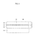
- FIG. 5 is a cross section of a halftone phase shift blank photomask.
- FIGS. 6A-6H are cross sections illustrating processing steps in the fabrication of halftone phase shift photomask in accordance with some embodiments of the inventive concept.
- first, second, third, etc. may be used herein to describe various elements, components, regions, layers and/or sections, these elements, components, regions, layers and/or sections should not be limited by these terms. These terms are only used to distinguish one element, component, region, layer or section from another region, layer or section. Thus, a first element, component, region, layer or section discussed below could be termed a second element, component, region, layer or section without departing from the teachings of the present inventive concept.
- spatially relative terms such as “beneath,” “below,” “lower,” “above,” “upper” and the like, may be used herein for ease of description to describe one element's or feature's relationship to another element(s) or feature(s) as illustrated in the figures. It will be understood that the spatially relative terms are intended to encompass different orientations of the device in use or operation in addition to the orientation depicted in the figures. For example, if the device in the figures is turned over, elements described as “below” or “beneath” other elements or features would then be oriented “above” the other elements or features. Thus, the term “below” can encompass both an orientation of above and below. The device may be otherwise oriented (rotated 90 degrees or at other orientations) and the spatially relative descriptors used herein interpreted accordingly.
- Embodiments are described herein with reference to cross-sectional illustrations that are schematic illustrations of idealized embodiments (and intermediate structures). As such, variations from the shapes of the illustrations as a result, for example, of manufacturing techniques and/or tolerances, are to be expected. Thus, embodiments should not be construed as limited to the particular shapes of regions illustrated herein but are to include deviations in shapes that result, for example, from manufacturing. For example, an implanted region illustrated as a rectangle will, typically, have rounded or curved features and/or a gradient of implant concentration at its edges rather than a binary change from implanted to non-implanted region. Likewise, a buried region formed by implantation may result in some implantation in the region between the buried region and the surface through which the implantation takes place. Thus, the regions illustrated in the figures are schematic in nature and their shapes are not intended to illustrate the actual shape of a region of a device and are not intended to limit the scope of the present inventive concept.
- embodiments the present inventive concept relate to halftone phase shift blank photomasks, halftone phase shift photomasks, and related methods of fabrication.
- FIG. 1 is a cross section illustrating a halftone phase shift photomask according to some embodiments of the inventive concept.
- FIG. 2 is a cross section of a halftone phase shift photomask having a sub-resolution assist feature (SRAF) pattern according to some embodiments of the inventive concept.
- FIG. 3 is a graph illustrating the relationship between the thicknesses of molybdenum silicon oxynitride (MoSiON) and Chromium (Cr) and optical transmittance in a blind area according to some embodiments of the inventive concept.
- FIG. 4 is a graph illustrating the relationship between the thicknesses of MoSiON and Cr and optical density in a blind area according to some embodiments of the inventive concept.
- a photomask 100 includes a pattern area P disposed at the center thereof and a blind area B disposed around the pattern area P.
- the pattern area P includes a main pattern 126 , such as a circuit pattern (e.g., a contact pattern or interconnection pattern), to be transferred to a wafer.
- the blind area B may include an alignment key (not shown) by which the photomask 100 is aligned with an exposure apparatus.
- the photomask 100 includes a transparent substrate 110 adapted to transmit the light, a light shielding pattern 142 adapted to shield the light, and shift patterns 124 and 126 interposed between the transparent substrate 110 and the light shielding pattern 142 and adapted to transmit the light in a predetermined ratio.
- the shift patterns 124 and 126 include a first shift pattern 124 disposed in the blind area B and a second shift pattern 126 disposed in the pattern area P.
- the blind area B has a transmittance of about zero percent to reduce, or possibly prevent, the light from being transmitted through the edge of the photomask 100 during exposure, thereby functioning to form a precise pattern on the wafer.
- an optical density of the blind area B may be greater than about 2.5 to reduce, or possibly prevent, unnecessary light from being transmitted to the wafer during exposure, and may be greater than about 3.0 for safety in some embodiments.
- the thickness of the light shielding pattern 142 gradually decreases, and it may be difficult to ensure an optical density.
- the sum of the thickness of the light shielding pattern 142 and the thickness of the first shift pattern 124 is about 1090 ⁇ or more in the blind area B to increase the likelihood of an optical density of 2.5 or more.
- the thickness of the light shielding pattern 142 does not typically exceed 160 ⁇ in the blind area B.
- the second shift pattern 126 has first and second portions in the pattern area P, a main pattern portion 126 a and an SRAF portion 126 b .
- an SRAF pattern 126 b may be additionally used.
- An SRAF pattern 126 b is an auxiliary pattern of a limited resolution or less, and functions to correct an optical proximity effect (OPE).
- the width of a critical dimension of the SRAF pattern 126 b is smaller than that of a critical dimension of the main pattern 126 a , it is important to form the SRAF pattern 126 b , and it is more difficult to increase the resolution of the SRAF pattern 126 b .
- the width of a critical dimension of the SRAF pattern 126 b is reduced to about half the width of a critical dimension of the main pattern 126 a with decrease in design rule, it is difficult to form the SRAF pattern 126 b using current photomask manufacturing technology.
- a photomask is manufactured, it is very important to set several exposure conditions to stably form the SRAF pattern 126 b.
- a thick light shielding layer may be used to increase the likelihood of an optical density of 2.5 or more in the blind area B, as mentioned above, a resist layer sufficiently thick in proportion to the light shielding layer is used to etch the thick light shielding layer.
- a resist layer sufficiently thick in proportion to the light shielding layer is used to etch the thick light shielding layer.
- an aspect ratio of the SRAF pattern 126 b is 1:2.5 (bottom:height) or more
- the SRAF pattern 126 b easily collapses. In particular, this is remarkable in a 45 nm pattern manufacturing process.
- there is a predetermined limit to increasing a thickness T 1 of a first resist layer see 150 of FIG. 5 ).
- the thickness T 1 of the first resist layer 150 exceeds 1500 ⁇ , it is difficult to form a fine pattern.
- the thickness T 1 of the first resist layer 150 may be determined within a range of from about 1000 ⁇ to about 1200 ⁇ .
- a thickness T 2 of a light shielding layer may also need to be reduced to satisfy the requirements of a thin film resist.
- the thickness T 2 of the light shielding layer 140 may be determined within a range of from about 100 ⁇ to about 160 ⁇ .
- the thickness T 2 of the light shielding pattern 142 needs to be reduced, the overall thickness T 2 +T 3 of the blind area B needs to be increased.
- the thickness T 2 of the light shielding pattern 142 is reduced and a thickness T 3 of the first shift pattern 124 is increased at least in the blind area B.
- the thickness T 3 of the first shift pattern 124 is greater than about 930 ⁇ .
- the thickness T 3 of the first shift pattern 124 in the blind area B is different from a thickness T 4 of the second shift pattern 126 in the pattern area P.
- the thickness T 4 of the second shift pattern 126 may not exceed 720 ⁇ , unlike the first shift pattern 124 .
- the thickness T 4 of the second shift pattern 126 may be determined to be about 660 ⁇ so that light maintains a phase difference of from about 90° to about 270° between the second shift pattern 126 having a transmittance of from about 1.0% to about 30% to the light and a second shift opening 134 defined by the shift pattern 126 .
- the thickness T 4 of the second shift pattern 126 tends to be gradually reduced from about 720 ⁇ to about 590 ⁇ or about 480 ⁇ .
- the second shift pattern 126 has a thickness of about 660 ⁇ .
- the thickness of each pattern for ensuring an optical density may vary.
- the relationship between the optical density and the thickness of each pattern may be observed when MoSiON is used for the shift patterns 124 and 126 and Cr is used for the light shielding pattern 142 .
- a graph of FIG. 3 can be obtained by calculating optical transmittance using equation 1. Also, a graph of FIG. 4 can be obtained by calculating optical density using equation 2.
- the optical density of the blind area B can be adjusted.
- the thickness of MoSiON is 1200 ⁇ and the thickness of Cr is increased from 100 ⁇ to 160 ⁇ , 180 ⁇ , and then 200 ⁇
- the optical density increases from 2.5 to 3.0.
- the thickness of Cr is 160 ⁇ and the thickness of MoSiON is increased from 1200 ⁇ to 1300 ⁇
- the optical density increases from 2.7 to 3.0.
- the thickness of MoSiON doubles from a generally used value of 660 ⁇ to 1320 ⁇ , it is possible to ensure an optical density of 3.0 or more even under the condition of the thickness of Cr being 160 ⁇ .
- the thickness T 3 of MoSiON in the blind area B is 1320 ⁇ and the thickness T 4 of MoSiON in the pattern area P is 660 ⁇ , it is possible to realize a phase difference of 180° in the pattern area P while ensuring an optical density of 3.0 or more in the blind area B because the thickness T 3 of MoSiON in the blind area B becomes at least two times the thickness T 4 of MoSiON in the pattern area P.
- the thickness T 4 of the second shift pattern 126 is reduced to form a fine pattern in the pattern area P, and the thickness T 3 of the first shift pattern 124 is increased in the blind area B to maintain an optimum optical density, so that the conflicting goals can be achieved.
- Halftone phase shift blank photomasks and methods of manufacturing halftone phase shift photomasks according to some embodiments of the inventive concept will be discussed below with reference to drawings.
- FIG. 5 is a cross section of a halftone phase shift blank photomask and FIGS. 6A to 6H are cross sections illustrating processing steps in the fabrication of halftone phase shift photomask in accordance with some embodiments of the inventive concept.
- a blank photomask 102 includes the transparent substrate 110 , a shift layer 120 stacked on the transparent substrate 110 , the light shielding layer 140 stacked on the shift layer 120 , and the first resist layer 150 stacked on the light shielding layer 140 .
- an anti-reflective layer ARL
- the transparent substrate 110 may be a transparent crystalline quartz (Qz) or glass through which light can be transmitted.
- the shift layer 120 may include a material such as molybdenum silicon nitride (MoSiN), molybdenum silicon carbonitride (MoSiCN), molybdenum silicon oxynitride (MoSiON), or molybdenum silicon carbon oxynitride (MoSiCON).
- MoSiN molybdenum silicon nitride
- MoSiCN molybdenum silicon carbonitride
- MoSiON molybdenum silicon oxynitride
- MoSiCON molybdenum silicon carbon oxynitride
- Chromium (Cr), chromium carbide (CrC), chromium nitride (CrN), chromium carbonitride (CrCN), etc. may be used for the light shielding layer 140 .
- the light shielding layer 140 may be formed to a thickness of from about 100 ⁇ to about 160 ⁇ to implement the thin first resist layer 150 .
- a positive or negative photosensitive film may be used as the first resist layer 150 .
- the first resist layer 150 have a thickness of from about 1000 ⁇ to about 1200 ⁇ to improve the resolution of a pattern and reduce the size of the pattern.
- a first exposure and development process is performed on the first resist layer 150 using an electron beam.
- the first resist layer 150 may be selectively patterned to form a first resist pattern 152 in the pattern area P.
- the first resist pattern 152 defines a first resist opening 156 , and may be formed as a hole type to form a contact pattern or formed as a line-and-space type to form an interconnection pattern.
- the light shielding layer 140 is dry-etched using the first resist pattern 152 as an etch mask.
- the light shielding pattern 142 that selectively exposes the shift layer 120 is formed.
- the first resist pattern 152 is stripped and cleaned and the shift layer 120 is partially or half-etched using the light shielding pattern 142 as a hard mask, thereby forming a half shift pattern 122 that defines the half shift opening 132 as illustrated in FIG. 6D .
- half refers to partial or less than all and not necessarily 50% or 1 ⁇ 2.
- the degree of half-etching is a ratio in which the shift layer 120 , an etch target layer, is partially, but not completely, etched.
- the degree of half-etching may denote that a portion of the shift layer 120 in the half shift opening 132 left without being etched has a height equal to a difference t between the thickness T 3 of the first shift pattern 124 in the blind area B and the thickness T 4 of the shift pattern 126 in the pattern area P as illustrated in FIG. 1 .
- the half shift pattern 122 may be formed as a predetermined contact pattern or interconnection pattern.
- the half shift pattern 122 has the thickness T 3 , which is thicker than the thickness T 4 of the second shift pattern 126 to be formed in the later process ( FIG. 6H ), by the difference t.
- the half shift opening 132 does not expose a surface of the transparent substrate 110 .
- an etching end time may be appropriately set to determine a ratio in which a part of the shift layer 120 is recessed, that is, the degree of half-etching.
- the degree of half-etching is determined to be half the thickness of the shift layer 120
- the depth D of the half shift opening 132 becomes the same as the height H left after the recess process
- the thickness T 4 of the second shift pattern 126 becomes half the thickness T 3 of the half shift pattern 122 .
- the thickness T 3 of the first shift pattern 124 in the blind area B may be double the thickness T 4 of the second shift pattern 126 in the pattern area P
- an optical density in the blind area B may be 3.0 or more
- a phase difference in the pattern area P may be 180°.
- the degree of half-etching is 1 ⁇ 2 in the drawings, however, embodiments are not limited to this configuration.
- a second resist layer (not shown) is stacked, and a photolithography process of opening the pattern area P is performed.
- a second exposure and development process is performed on the second resist layer to form a second resist pattern 162 defining a second resist opening 166 .
- an etching process is performed using the second resist pattern 162 as an etch mask to strip the light shielding pattern 142 in the pattern area P.
- the second resist pattern 162 is stripped as illustrated in FIG. 6G .
- the light shielding pattern 142 in the blind area B remains as is.
- an etching process is performed using the light shielding pattern 142 in the blind area B as an etch mask to reduce the height of the half shift pattern 122 in the pattern area P.
- the second shift pattern 126 is formed in the pattern area P.
- the half shift pattern 122 in the pattern area P is removed by the thickness t, so that the thickness T 4 of the half shift pattern 122 is reduced to the thickness T 3 of the second shift pattern 126 and the thickness T 3 of the portion in the half shift opening 132 is substantially removed.
- the second shift opening 134 is formed, and the transparent substrate 110 is exposed.
- the substrate 110 may be exposed through the half shift opening 132 .
- the etching end time in the etching process may be a time point when the transparent substrate 110 is exposed through the bottom surface of the half shift opening 132 formed while the etching process is performed.
- a shift pattern in a blind area may become thicker than a conventional shift pattern to increase the likelihood of an optical density of 3.0 or more, and the thickness of the shift pattern in a pattern area is maintained as is to realize a phase difference of 180°.
- the shift pattern in the blind area becomes thicker, the likelihood of an optical density can be increased as is, and as a result, a light shielding pattern can become a thin film.
- the light shielding pattern becomes a thin film, a resist layer functioning as a mask can also become a thin film, and the resolution of the pattern can be improved.
Landscapes
- Physics & Mathematics (AREA)
- General Physics & Mathematics (AREA)
- Preparing Plates And Mask In Photomechanical Process (AREA)
- Exposure And Positioning Against Photoresist Photosensitive Materials (AREA)
Abstract
Description
transmittance=exp(−2π/λ×2k×thickness)
optical density=log(−Δtransmittance)
Claims (19)
Priority Applications (1)
| Application Number | Priority Date | Filing Date | Title |
|---|---|---|---|
| US13/706,978 US8865375B2 (en) | 2009-10-30 | 2012-12-06 | Halftone phase shift blank photomasks and halftone phase shift photomasks |
Applications Claiming Priority (4)
| Application Number | Priority Date | Filing Date | Title |
|---|---|---|---|
| KR1020090104504A KR101656456B1 (en) | 2009-10-30 | 2009-10-30 | Half-tone phase shift photomask blank and half-tone phase shift photomask and methods of fabricating the same |
| KR10-2009-0104504 | 2009-10-30 | ||
| US12/909,395 US8329363B2 (en) | 2009-10-30 | 2010-10-21 | Methods of fabricating halftone phase shift blank photomasks and halftone phase shift photomasks |
| US13/706,978 US8865375B2 (en) | 2009-10-30 | 2012-12-06 | Halftone phase shift blank photomasks and halftone phase shift photomasks |
Related Parent Applications (1)
| Application Number | Title | Priority Date | Filing Date |
|---|---|---|---|
| US12/909,395 Continuation US8329363B2 (en) | 2009-10-30 | 2010-10-21 | Methods of fabricating halftone phase shift blank photomasks and halftone phase shift photomasks |
Publications (2)
| Publication Number | Publication Date |
|---|---|
| US20130101926A1 US20130101926A1 (en) | 2013-04-25 |
| US8865375B2 true US8865375B2 (en) | 2014-10-21 |
Family
ID=43925804
Family Applications (2)
| Application Number | Title | Priority Date | Filing Date |
|---|---|---|---|
| US12/909,395 Active 2031-03-02 US8329363B2 (en) | 2009-10-30 | 2010-10-21 | Methods of fabricating halftone phase shift blank photomasks and halftone phase shift photomasks |
| US13/706,978 Active 2030-11-01 US8865375B2 (en) | 2009-10-30 | 2012-12-06 | Halftone phase shift blank photomasks and halftone phase shift photomasks |
Family Applications Before (1)
| Application Number | Title | Priority Date | Filing Date |
|---|---|---|---|
| US12/909,395 Active 2031-03-02 US8329363B2 (en) | 2009-10-30 | 2010-10-21 | Methods of fabricating halftone phase shift blank photomasks and halftone phase shift photomasks |
Country Status (3)
| Country | Link |
|---|---|
| US (2) | US8329363B2 (en) |
| JP (1) | JP5662101B2 (en) |
| KR (1) | KR101656456B1 (en) |
Families Citing this family (6)
| Publication number | Priority date | Publication date | Assignee | Title |
|---|---|---|---|---|
| JP5286455B1 (en) | 2012-03-23 | 2013-09-11 | Hoya株式会社 | Mask blank, transfer mask, and manufacturing method thereof |
| JP5686216B1 (en) * | 2013-08-20 | 2015-03-18 | 大日本印刷株式会社 | Mask blank, phase shift mask, and manufacturing method thereof |
| KR102260188B1 (en) * | 2014-04-08 | 2021-06-04 | 다이니폰 인사츠 가부시키가이샤 | Mask blank, phase shift mask, and phase-shift mask manufacturing method |
| JP6524614B2 (en) * | 2014-05-27 | 2019-06-05 | 大日本印刷株式会社 | Mask blanks, mask blanks with negative resist film, phase shift mask, and method of manufacturing patterned body using the same |
| CN104849958B (en) * | 2015-05-29 | 2019-04-05 | 京东方科技集团股份有限公司 | A semi-transparent and semi-shielding panel, a touch panel, a manufacturing method thereof, and a display device |
| US11226562B2 (en) * | 2018-09-20 | 2022-01-18 | Taiwan Semiconductor Manufacturing Company Ltd. | Semiconductor structure and manufacturing method thereof |
Citations (7)
| Publication number | Priority date | Publication date | Assignee | Title |
|---|---|---|---|---|
| KR0166854B1 (en) | 1996-06-27 | 1999-01-15 | 문정환 | How to fix defects in phase inversion mask |
| JP2001188335A (en) | 1999-12-28 | 2001-07-10 | Toshiba Corp | Exposure mask and pattern forming method using the same |
| US20010009745A1 (en) * | 2000-01-18 | 2001-07-26 | Kim Hyoung-Joon | Half tone phase shift mask having a stepped aperture |
| US20050069788A1 (en) * | 2003-09-30 | 2005-03-31 | Renesas Technology Corp. | Photomask, photomask manufacturing method and semiconductor device manufacturing method using photomask |
| JP2008102402A (en) | 2006-10-20 | 2008-05-01 | Toppan Printing Co Ltd | Method for manufacturing halftone phase shift mask |
| JP2009080510A (en) | 2003-04-09 | 2009-04-16 | Hoya Corp | Photomask manufacturing method and photomask blank |
| US7678509B2 (en) | 2003-08-15 | 2010-03-16 | Hoya Corporation | Method of producing phase shift masks |
Family Cites Families (3)
| Publication number | Priority date | Publication date | Assignee | Title |
|---|---|---|---|---|
| US7442472B2 (en) * | 2004-08-10 | 2008-10-28 | Micron Technology, Inc. | Methods of forming reticles |
| JP2007279440A (en) * | 2006-04-07 | 2007-10-25 | Toshiba Corp | Halftone phase shift mask and manufacturing method thereof |
| JP5067313B2 (en) * | 2008-08-19 | 2012-11-07 | 富士通セミコンダクター株式会社 | Method for manufacturing halftone phase shift mask and method for manufacturing semiconductor device |
-
2009
- 2009-10-30 KR KR1020090104504A patent/KR101656456B1/en active Active
-
2010
- 2010-10-18 JP JP2010233841A patent/JP5662101B2/en active Active
- 2010-10-21 US US12/909,395 patent/US8329363B2/en active Active
-
2012
- 2012-12-06 US US13/706,978 patent/US8865375B2/en active Active
Patent Citations (7)
| Publication number | Priority date | Publication date | Assignee | Title |
|---|---|---|---|---|
| KR0166854B1 (en) | 1996-06-27 | 1999-01-15 | 문정환 | How to fix defects in phase inversion mask |
| JP2001188335A (en) | 1999-12-28 | 2001-07-10 | Toshiba Corp | Exposure mask and pattern forming method using the same |
| US20010009745A1 (en) * | 2000-01-18 | 2001-07-26 | Kim Hyoung-Joon | Half tone phase shift mask having a stepped aperture |
| JP2009080510A (en) | 2003-04-09 | 2009-04-16 | Hoya Corp | Photomask manufacturing method and photomask blank |
| US7678509B2 (en) | 2003-08-15 | 2010-03-16 | Hoya Corporation | Method of producing phase shift masks |
| US20050069788A1 (en) * | 2003-09-30 | 2005-03-31 | Renesas Technology Corp. | Photomask, photomask manufacturing method and semiconductor device manufacturing method using photomask |
| JP2008102402A (en) | 2006-10-20 | 2008-05-01 | Toppan Printing Co Ltd | Method for manufacturing halftone phase shift mask |
Also Published As
| Publication number | Publication date |
|---|---|
| KR20110047756A (en) | 2011-05-09 |
| US20110104591A1 (en) | 2011-05-05 |
| KR101656456B1 (en) | 2016-09-12 |
| JP2011095744A (en) | 2011-05-12 |
| US8329363B2 (en) | 2012-12-11 |
| US20130101926A1 (en) | 2013-04-25 |
| JP5662101B2 (en) | 2015-01-28 |
Similar Documents
| Publication | Publication Date | Title |
|---|---|---|
| KR101135246B1 (en) | Method of producing photomask and photomask blank | |
| KR100775382B1 (en) | Method of manufacturing a mask blank, a phase shift mask and a template | |
| KR101676082B1 (en) | Photo mask blank, method for manufacturing photo mask, and method for manufacturing phase shift mask | |
| US8865375B2 (en) | Halftone phase shift blank photomasks and halftone phase shift photomasks | |
| KR102195696B1 (en) | Halftone phase shift photomask blank | |
| KR101319659B1 (en) | Photomask blank, photomask manufacturing method and semiconductor device manufacturing method | |
| KR102249017B1 (en) | Photomask blank | |
| US20180267398A1 (en) | Photomask blank, method for manufacturing photomask, and mask pattern formation method | |
| KR101407230B1 (en) | Blankmask, Photomask and method for fabricating the same | |
| JP6573591B2 (en) | Photomask manufacturing method, photomask, and display device manufacturing method | |
| US6410191B1 (en) | Phase-shift photomask for patterning high density features | |
| US5888678A (en) | Mask and simplified method of forming a mask integrating attenuating phase shifting mask patterns and binary mask patterns on the same mask substrate | |
| US8592105B2 (en) | Photomasks and methods of fabricating the same | |
| US9057961B2 (en) | Systems and methods for lithography masks | |
| US7838173B2 (en) | Structure design and fabrication on photomask for contact hole manufacturing process window enhancement | |
| US20030226819A1 (en) | Single trench alternating phase shift mask fabrication | |
| US20040180548A1 (en) | Dual trench alternating phase shift mask fabrication | |
| US6562521B1 (en) | Semiconductor feature having support islands | |
| US6296987B1 (en) | Method for forming different patterns using one mask | |
| US7445159B2 (en) | Dual trench alternating phase shift mask fabrication | |
| KR20010019170A (en) | Method for fabricating photomask and structure thereof |
Legal Events
| Date | Code | Title | Description |
|---|---|---|---|
| AS | Assignment |
Owner name: SAMSUNG ELECTRONICS CO., LTD., KOREA, REPUBLIC OF Free format text: ASSIGNMENT OF ASSIGNORS INTEREST;ASSIGNORS:JANG, IL-YONG;KIM, HOON;LEE, HYE-KYOUNG;AND OTHERS;REEL/FRAME:030013/0055 Effective date: 20130227 |
|
| AS | Assignment |
Owner name: SAMSUNG ELECTRONICS CO., LTD., KOREA, REPUBLIC OF Free format text: DUTY INVENTION ASSIGNMENT;ASSIGNOR:WOO, SANG-GYUN;REEL/FRAME:030091/0812 Effective date: 20091102 |
|
| STCF | Information on status: patent grant |
Free format text: PATENTED CASE |
|
| MAFP | Maintenance fee payment |
Free format text: PAYMENT OF MAINTENANCE FEE, 4TH YEAR, LARGE ENTITY (ORIGINAL EVENT CODE: M1551) Year of fee payment: 4 |
|
| MAFP | Maintenance fee payment |
Free format text: PAYMENT OF MAINTENANCE FEE, 8TH YEAR, LARGE ENTITY (ORIGINAL EVENT CODE: M1552); ENTITY STATUS OF PATENT OWNER: LARGE ENTITY Year of fee payment: 8 |
|
| MAFP | Maintenance fee payment |
Free format text: PAYMENT OF MAINTENANCE FEE, 12TH YEAR, LARGE ENTITY (ORIGINAL EVENT CODE: M1553); ENTITY STATUS OF PATENT OWNER: LARGE ENTITY Year of fee payment: 12 |