US8862005B2 - Image forming apparatus - Google Patents
Image forming apparatus Download PDFInfo
- Publication number
- US8862005B2 US8862005B2 US13/749,907 US201313749907A US8862005B2 US 8862005 B2 US8862005 B2 US 8862005B2 US 201313749907 A US201313749907 A US 201313749907A US 8862005 B2 US8862005 B2 US 8862005B2
- Authority
- US
- United States
- Prior art keywords
- developer
- toner
- developer transport
- voltages
- waveforms
- Prior art date
- Legal status (The legal status is an assumption and is not a legal conclusion. Google has not performed a legal analysis and makes no representation as to the accuracy of the status listed.)
- Active, expires
Links
Images


Classifications
-
- G03G15/0825—
-
- G—PHYSICS
- G03—PHOTOGRAPHY; CINEMATOGRAPHY; ANALOGOUS TECHNIQUES USING WAVES OTHER THAN OPTICAL WAVES; ELECTROGRAPHY; HOLOGRAPHY
- G03G—ELECTROGRAPHY; ELECTROPHOTOGRAPHY; MAGNETOGRAPHY
- G03G15/00—Apparatus for electrographic processes using a charge pattern
- G03G15/06—Apparatus for electrographic processes using a charge pattern for developing
- G03G15/08—Apparatus for electrographic processes using a charge pattern for developing using a solid developer, e.g. powder developer
- G03G15/0822—Arrangements for preparing, mixing, supplying or dispensing developer
- G03G15/0848—Arrangements for testing or measuring developer properties or quality, e.g. charge, size, flowability
- G03G15/0849—Detection or control means for the developer concentration
- G03G15/0853—Detection or control means for the developer concentration the concentration being measured by magnetic means
-
- G—PHYSICS
- G03—PHOTOGRAPHY; CINEMATOGRAPHY; ANALOGOUS TECHNIQUES USING WAVES OTHER THAN OPTICAL WAVES; ELECTROGRAPHY; HOLOGRAPHY
- G03G—ELECTROGRAPHY; ELECTROPHOTOGRAPHY; MAGNETOGRAPHY
- G03G15/00—Apparatus for electrographic processes using a charge pattern
- G03G15/06—Apparatus for electrographic processes using a charge pattern for developing
- G03G15/08—Apparatus for electrographic processes using a charge pattern for developing using a solid developer, e.g. powder developer
- G03G15/0806—Apparatus for electrographic processes using a charge pattern for developing using a solid developer, e.g. powder developer on a donor element, e.g. belt, roller
-
- G—PHYSICS
- G03—PHOTOGRAPHY; CINEMATOGRAPHY; ANALOGOUS TECHNIQUES USING WAVES OTHER THAN OPTICAL WAVES; ELECTROGRAPHY; HOLOGRAPHY
- G03G—ELECTROGRAPHY; ELECTROPHOTOGRAPHY; MAGNETOGRAPHY
- G03G15/00—Apparatus for electrographic processes using a charge pattern
- G03G15/06—Apparatus for electrographic processes using a charge pattern for developing
- G03G15/08—Apparatus for electrographic processes using a charge pattern for developing using a solid developer, e.g. powder developer
- G03G15/0822—Arrangements for preparing, mixing, supplying or dispensing developer
- G03G15/0848—Arrangements for testing or measuring developer properties or quality, e.g. charge, size, flowability
- G03G15/0849—Detection or control means for the developer concentration
- G03G15/0851—Detection or control means for the developer concentration the concentration being measured by electrical means
-
- G—PHYSICS
- G03—PHOTOGRAPHY; CINEMATOGRAPHY; ANALOGOUS TECHNIQUES USING WAVES OTHER THAN OPTICAL WAVES; ELECTROGRAPHY; HOLOGRAPHY
- G03G—ELECTROGRAPHY; ELECTROPHOTOGRAPHY; MAGNETOGRAPHY
- G03G15/00—Apparatus for electrographic processes using a charge pattern
- G03G15/06—Apparatus for electrographic processes using a charge pattern for developing
- G03G15/08—Apparatus for electrographic processes using a charge pattern for developing using a solid developer, e.g. powder developer
- G03G15/0822—Arrangements for preparing, mixing, supplying or dispensing developer
- G03G15/0887—Arrangements for conveying and conditioning developer in the developing unit, e.g. agitating, removing impurities or humidity
- G03G15/0891—Arrangements for conveying and conditioning developer in the developing unit, e.g. agitating, removing impurities or humidity for conveying or circulating developer, e.g. augers
-
- G—PHYSICS
- G03—PHOTOGRAPHY; CINEMATOGRAPHY; ANALOGOUS TECHNIQUES USING WAVES OTHER THAN OPTICAL WAVES; ELECTROGRAPHY; HOLOGRAPHY
- G03G—ELECTROGRAPHY; ELECTROPHOTOGRAPHY; MAGNETOGRAPHY
- G03G15/00—Apparatus for electrographic processes using a charge pattern
- G03G15/06—Apparatus for electrographic processes using a charge pattern for developing
- G03G15/08—Apparatus for electrographic processes using a charge pattern for developing using a solid developer, e.g. powder developer
- G03G15/0896—Arrangements or disposition of the complete developer unit or parts thereof not provided for by groups G03G15/08 - G03G15/0894
Definitions
- the present invention relates to an image forming apparatus.
- an image forming apparatus includes a latent image carrier that rotates and that has a surface on which an electrostatic latent image to be developed by a charged toner is formed; a container that contains a developer including the toner; plural developer transport members disposed side by side so that peripheral surfaces thereof face the latent image carrier and so that the peripheral surfaces of adjacent ones thereof face each other, the developer transport members distributing the developer supplied from the container among one another and transporting the developer to the surface of the latent image carrier by carrying the developer on the peripheral surfaces and rotating in circumferential directions of the peripheral surfaces; a power supply that supplies voltages having plural waveforms having an identical period to the plural developer transport members; a detector that detects a toner concentration of the developer contained in the container; and a controller.
- the controller performs control so that the power supply supplies to the plural developer transport members, when the toner concentration detected by the detector is higher than a predetermined upper limit, voltages having the waveforms that generate a potential difference therebetween, the potential difference causing the toner concentration of the developer distributed to a most downstream developer transport member to decrease and the toner concentration of the developer distributed to at least one of the developer transport members that is disposed upstream of the most downstream developer transport member to increase, the most downstream developer transport member being one of the developer transport members that is disposed at a most downstream position in a movement direction in which a region on the surface of the latent image carrier facing the plural developer transport members moves.
- FIG. 1 is a schematic view of an image forming apparatus according to a first exemplary embodiment of the present invention
- FIG. 2 is a sectional view of a developing device illustrated in FIG. 1 ;
- FIG. 3 is a diagram illustrating the waveforms of voltages supplied by power supplies
- FIG. 4 is a flowchart of an operation of the image forming apparatus illustrated in FIG. 1 ;
- FIG. 5 is a diagram illustrating the waveforms of voltages supplied to a downstream roller and an upstream roller according to a second exemplary embodiment
- FIG. 6 is a schematic sectional view of a developing device according to a third exemplary embodiment
- FIG. 7 is a chart illustrating the relationship between the toner concentration of a developer in a container and the trends of the toner concentrations of the developer supported on three development rollers;
- FIGS. 8A and 8B are diagrams illustrating the waveforms of voltages according to the third exemplary embodiment
- FIG. 9 is flowchart of an operation of an image forming apparatus according to the third exemplary embodiment.
- FIGS. 10A and 10B are diagrams illustrating the waveforms of voltages supplied to the downstream roller, the center roller, and the upstream roller according to a fourth exemplary embodiment.
- FIG. 1 is a schematic view of an image forming apparatus according to a first exemplary embodiment of the present invention.
- An image forming apparatus 1 illustrated in FIG. 1 is a tandem-type color printer in which image forming units 10 Y, 10 M, 10 C, and 10 K for yellow (Y), magenta (M), cyan (C), and black (K) are parallelly arranged.
- the image forming apparatus 1 is capable of printing a single-color image and a full-color image composed of four color toner images.
- Toner cartridges 18 Y, 18 M, 18 C, and 18 K contain yellow, magenta, cyan, and black toners.
- the image forming unit 10 Y includes a photoconductor drum 11 Y, a charger 12 Y, an exposure unit 13 Y, a developing device 20 Y, a first transfer unit 15 Y, and a photoconductor cleaner 16 Y.
- the photoconductor drum 11 Y includes a cylindrical body and a photoconductor layer disposed on a surface of the cylindrical body.
- the photoconductor drum 11 Y holds an image on a surface thereof and rotates around an axis in the direction of arrow A.
- the charger 12 Y, the exposure unit 13 Y, the developing device 20 Y, the first transfer unit 15 Y, and the photoconductor cleaner 16 Y are disposed so as to surround the photoconductor drum 11 Y in the direction of arrow A.
- the charger 12 Y charges the surface of the photoconductor drum 11 Y.
- the charger 12 Y is a charging roller that contacts the surface of the photoconductor drum 11 Y.
- a voltage having a polarity the same as the polarity of a toner used in the developing device 20 Y is applied to the charger 12 Y.
- the charger 12 Y charges the surface of the photoconductor drum 11 Y that is in contact with the charger 12 Y.
- the exposure unit 13 Y performs exposure by irradiating the surface of the photoconductor drum 11 Y with light.
- the exposure unit 13 Y emits a laser beam in accordance with an image signal supplied to the image forming apparatus 1 from the outside, and scans the photoconductor drum 11 Y with the laser beam.
- the developing device 20 Y develops the surface of the photoconductor drum 11 Y by using a developer.
- the toner cartridge 18 Y supplies a toner to the developing device 20 Y.
- the developing device 20 Y agitates the developer, in which the toner and a magnetic carrier are mixed together, and thereby charges the toner and the magnetic carrier, and develops the surface of the photoconductor drum 11 Y using the charged toner.
- the first transfer unit 15 Y is a roller that faces the photoconductor drum 11 Y with an intermediate transfer belt 30 therebetween.
- the first transfer unit 15 Y to which a voltage relative to the photoconductor drum 11 Y is applied, transfers a toner image on the photoconductor drum 11 Y to the intermediate transfer belt 30 .
- the photoconductor cleaner 16 Y cleans the surface of the photoconductor drum 11 Y by removing waste substances such as toner that remains on a part of the surface of the photoconductor drum 11 Y on which the first transfer unit 15 Y has performed a transfer operation.
- the image forming apparatus 1 further includes the intermediate transfer belt 30 , a fixing unit 60 , a sheet transport unit 80 , and a controller 1 A.
- the intermediate transfer belt 30 is an endless belt that is looped over belt support rollers 31 to 35 .
- the intermediate transfer belt 30 rotates in the direction of arrow B and moves past the image forming units 10 Y, 10 M, 10 C, 10 K, and a second transfer unit 50 .
- Color toner images are transferred to the intermediate transfer belt 30 from the image forming units 10 Y, 10 M, 10 C, and 10 K.
- the intermediate transfer belt 30 moves while carrying the color toner images thereon.
- the second transfer unit 50 is a roller that rotates with the intermediate transfer belt 30 and a sheet P interposed between the second transfer unit 50 and a backup roller 34 , which is one of the belt support rollers 31 to 35 .
- the second transfer unit 50 to which a voltage having a polarity opposite to that of the toner is applied, transfers a toner image from the intermediate transfer belt 30 to the sheet P.
- the fixing unit 60 fixes a toner image to the sheet P.
- the fixing unit 60 includes a pressing roller 62 and a heating roller 61 , in which a heater is disposed.
- the heating roller 61 and the pressing roller 62 heat and press the toner of an unfixed toner image formed on the sheet P by pressing the sheet P while the sheet P passes through a gap therebetween, and thereby fix the toner image to the sheet P.
- the sheet transport unit 80 transfers the sheet P along a sheet transport path R, which extends through the second transfer unit 50 and the fixing unit 60 .
- the sheet transport unit 80 includes a pick-up roller 81 , transport rollers 82 , registration rollers 84 , and output rollers 86 .
- the pick-up roller 81 picks up the sheet P contained in the sheet container T, and the transport rollers 82 transport the sheet P.
- the registration rollers 84 transport the sheet P to the second transfer unit 50 , and the output rollers 86 output the sheet P to the outside.
- the photoconductor drum 11 Y rotates in the direction of arrow A, and the charger 12 Y charges the surface of the photoconductor drum 11 Y.
- the exposure unit 13 Y irradiates the photoconductor drum 11 Y with light in accordance with data for yellow included in an image signal.
- the exposure unit 13 Y forms an electrostatic latent image on the surface of the photoconductor drum 11 Y by irradiating the surface of the photoconductor drum 11 Y with light based on an image signal for yellow included in the image signal supplied from the outside.
- the toner cartridge 18 Y supplies yellow toner to the developing device 20 Y.
- the developing device 20 Y forms a toner image by developing the electrostatic latent image on the photoconductor drum 11 Y using the toner.
- the photoconductor drum 11 Y rotates while holding the yellow toner image formed thereon.
- the first transfer unit 15 Y transfers the toner image formed on the surface of the photoconductor drum 11 Y to the intermediate transfer belt 30 .
- the photoconductor cleaner 16 Y removes toner remaining on the photoconductor drum 11 Y.
- the intermediate transfer belt 30 rotates in the direction of arrow B.
- the image forming units 10 M, 10 C, and 10 K for colors other than yellow form toner images of the other colors in the same way as the image forming unit 10 Y does, and transfers the toner images to the intermediate transfer belt 30 so as to overlap each other.
- the pick-up roller 81 picks up the sheet P from the sheet container T.
- the transport rollers 82 and the registration rollers 84 transport the sheet P along the sheet transport path R in the direction of arrow C toward the second transfer unit 50 .
- the registration rollers 84 transport the sheet P to the second transfer unit 50 on the basis of the timings at which the toner images are transferred to the intermediate transfer belt 30 .
- the second transfer unit 50 transfers the toner images from the intermediate transfer belt 30 to the sheet P.
- the sheet P, on which the toner images have been transferred, is transported from the second transfer unit 50 to the fixing unit 60 , and the transferred toner images are fixed to the sheet P. Thus, an image is formed on the sheet P.
- the output rollers 86 output the sheet P, on which an image has been formed, to the outside of the image forming apparatus 1 .
- a belt cleaner 70 removes toner remaining on the intermediate transfer belt 30 after the second transfer unit 50 has performed a transfer operation.
- FIG. 2 is a sectional view of the developing device illustrated in FIG. 1 .
- Power supplies 291 and 292 illustrated in FIG. 2 supply development bias voltages to the developing device 20 .
- the developing devices 20 Y to 20 K for respective colors illustrated in FIG. 1 which have the same structure, will be collectively described as the developing device 20 .
- the developing device 20 includes a container 21 , a downstream roller 22 , a first magnet 23 , an upstream roller 24 , a second magnet 25 , a first agitation member 26 A, a second agitation member 26 B, a paddle member 27 , and a toner concentration sensor 28 .
- the downstream roller 22 and the upstream roller 24 are respectively examples of a most downstream developer transport member and a most upstream developer transport member.
- the toner concentration sensor 28 is an example of a detector.
- the container 21 contains a developer and supports the members of the developing device 20 .
- the downstream roller 22 and the upstream roller 24 which are cylindrical development rollers extending in the axial direction Y, are disposed in the container 21 so that the peripheral surfaces thereof face the photoconductor drum 11 .
- the downstream roller 22 and the upstream roller 24 are disposed so that there is a gap between each of these rollers 22 and 24 and the photoconductor drum 11 .
- the downstream roller 22 is disposed downstream of the upstream roller 24 in a direction in which a peripheral surface of the photoconductor drum 11 , which rotates in the direction of arrow A, moves.
- the first magnet 23 which is disposed in the downstream roller 22 , attracts the developer toward the downstream roller 22 .
- the second magnet 25 which is disposed in the upstream roller 24 , attracts the developer toward the upstream roller 24 .
- the first magnet 23 has plural magnetic poles arranged in the circumferential direction of the downstream roller 22 .
- the second magnet 25 has plural magnetic poles arranged in the circumferential direction of the upstream roller 24 .
- Each of the downstream roller 22 and the upstream roller 24 rotates and thereby transports the developer in the container 21 to a surface of the photoconductor drum 11 .
- the downstream roller 22 rotates in the direction of arrow D
- the upstream roller 24 rotates in the direction of arrow E, which is opposite to the direction of arrow D. That is, the downstream roller 22 and the upstream roller 24 rotate so that parts of the peripheral surfaces thereof that face each other move in substantially the same direction.
- a part of the peripheral surface of the downstream roller 22 that faces a part the photoconductor drum 11 in a first development region d1 moves in a direction substantially the same as that of the part of the peripheral surface of the photoconductor drum 11 (“with”).
- a part of the peripheral surface of the upstream roller 24 that faces a part of the photoconductor drum 11 in a second development region d2 moves in a direction opposite to that of the part of the peripheral surface of the photoconductor drum 11 (“against”).
- the first agitation member 26 A and the second agitation member 26 B agitate the developer in the container 21 .
- Each of the first agitation member 26 A and the second agitation member 26 B has spiral blades disposed around a rotary shaft extending in the axial direction Y.
- the first agitation member 26 A and the second agitation member 26 B are disposed adjacent to each other, and the first agitation member 26 A is disposed adjacent to the downstream roller 22 .
- the first agitation member 26 A and the second agitation member 26 B rotate and thereby transport the developer in opposite directions along the axial direction Y.
- the developer circulates in the container 21 while being agitated by the first agitation member 26 A and the second agitation member 26 B.
- toner and magnetic carrier of the developer While being agitated, toner and magnetic carrier of the developer are charged with opposite polarities.
- the toner is negatively charged, and the magnetic carrier is positively charged.
- the toner concentration sensor 28 detects the toner concentration of the developer by detecting the magnetism of the magnetic carrier in the container 21 .
- the developer transported by the first agitation member 26 A is attracted to the downstream roller 22 , is supported on the downstream roller 22 , and moves in the direction of arrow D.
- a layer regulation member 205 which has a plate-like shape, is disposed near a part of the peripheral surface of the downstream roller 22 between the first agitation member 26 A and the upstream roller 24 .
- the layer regulation member 205 regulates the thickness, that is, the amount of the developer transported on the downstream roller 22 .
- a part of the developer is distributed to the upstream roller 24 in a region in which the downstream roller 22 and the upstream roller 24 face each other.
- the upstream roller 24 transports the developer distributed thereto to a second development region d2 of the photoconductor drum 11 .
- the downstream roller 22 transports the developer that remains on the downstream roller 22 to a first development region d1 of the photoconductor drum 11 .
- the developer is distributed on the basis of the magnetic forces of the first magnet 23 and the second magnet 25 and the electric potentials of the downstream roller 22 and the upstream roller 24 .
- the toner of the developer is negatively charged, if the potential difference (voltage) between the downstream roller 22 and the upstream roller 24 is greater than a movement threshold voltage, the toner tends to move toward one of the downstream and upstream rollers 22 and 24 having a higher potential (positive side). The greater the potential difference, the larger the amount of toner that moves.
- the toner concentration of the developer distributed to the downstream roller 22 and the upstream roller 24 are controlled by the voltages supplied by the power supplies 291 and 292 .
- the controller 1 A controls the voltage of DC component (mean value), the amplitude of AC component, and the phase of waveform of each of the voltages output from the power supplies 291 and 292 .
- the photoconductor drum 11 contacts the developer in the second development region d2 and the first development region d1.
- the toner of the developer adheres to an electrostatic latent image on the photoconductor drum 11 A, and thereby a toner image is formed.
- the developer that has not adhered to the photoconductor drum 11 in the first development region d1 is transported by the downstream roller 22 and is returned to the first agitation member 26 A.
- the developer that has not adhered to the photoconductor drum 11 in the second development region d2 is transported by the upstream roller 24 and is returned to the first agitation member 26 A.
- the peripheral surface of the upstream roller 24 moves in a direction opposite to that of the photoconductor drum 11 . Therefore, the upstream roller 24 has development ability that is higher than that of the downstream roller 22 , whose peripheral surface moves in a direction the same as that of the peripheral surface of the photoconductor drum 11 . That is, if conditions other than the rotation direction (for example, the electric potential) are the same, the upstream roller 24 causes a larger amount of toner to adhere to the photoconductor drum 11 than the downstream roller 22 does. However, the upstream roller 24 is more likely to cause toner fog, which is a phenomenon in which the toner adheres to a background region (non-image region) in which an electrostatic latent image has not been formed.
- toner fog is a phenomenon in which the toner adheres to a background region (non-image region) in which an electrostatic latent image has not been formed.
- downstream roller 22 is less likely to cause toner fog, although the development ability of the downstream roller 22 is lower than that of the upstream roller 24 .
- the downstream roller 22 is capable of preventing toner fog by attracting toner that the upstream roller 24 has caused to adhere to a background region.
- the upstream roller 24 which moves in a direction opposite to that of the photoconductor drum 11 , causes a large amount of toner to adhere to the photoconductor drum 11
- the downstream roller 22 which moves in a direction the same as that of the photoconductor drum 11 , prevents toner fog while compensating for shortage of toner in an image.
- the controller 1 A controls the voltages supplied by the power supplies 291 and 292 and thereby controls the amount of toner of the developer distributed by the downstream roller 22 and the upstream roller 24 .
- FIG. 3 is a diagram illustrating the waveforms of voltages supplied by the power supplies.
- FIG. 3 illustrates the waveform of a voltage Vdev1 supplied from the power supply 291 to the downstream roller 22 and the waveform of a voltage Vdev2 supplied from the power supply 292 to the upstream roller 24 .
- FIG. 3 also illustrates the electric potentials of the peripheral surfaces of the photoconductor drums 11 ( 11 Y to 11 K).
- each of the two power supplies 291 and 292 outputs a voltage in which an AC voltage is superimposed on a DC voltage.
- the DC voltage Vdc of the two power supplies 291 and 292 is a voltage between a charge potential VH, which is the potential of the peripheral surface of the photoconductor drum 11 (one of 11 Y to 11 K) that have been charged by the charger 12 (one of 12 Y to 12 K), and an exposure potential VL, which is the potential of the peripheral surface of the photoconductor drum 11 that has been exposed to light by the exposure unit 13 (one of 13 Y to 13 K).
- the waveforms of the two voltages Vdev1 and Vdev2 for one period are the same.
- the waveform for one period is asymmetric with respect to time.
- the waveform is a sawtooth wave.
- the waveforms of the AC components of the two voltages Vdev1 and Vdev2 are also the same.
- the waveforms of the two voltages Vdev1 and Vdev2 are the same waveforms whose phases are displaced from each other. As a result of the phase displacement, there are periods t1 in which the voltage Vdev2 of the upstream roller 24 is higher than (has a negative value whose absolute value is smaller than) the voltage Vdev1 of the downstream roller 22 .
- the amount of toner that moves to the upstream roller 24 increases in a region in which the upstream roller 24 and the downstream roller 22 face each other.
- periods t0 which are the periods excluding the periods t1
- the voltage Vdev1 of the downstream roller 22 is higher than the voltage Vdev2 of the upstream roller 24 .
- the (absolute value of the) voltage difference in the periods t0 is smaller than that in the periods t1.
- the difference between the voltages Vdev1 and Vdev2 in the periods t1 influences the movement of toner.
- the voltages Vdev1 and Vdev2 illustrated in FIG. 3 are supplied to the downstream roller 22 and the upstream roller 24 , the toner concentration of the developer distributed to the upstream roller 24 becomes higher than that of the developer distributed to the downstream roller 22 .
- the toner concentration of the developer distributed to the upstream roller 24 becomes substantially the same as that of the developer distributed to the downstream roller 22 .
- the waveform and amplitude of the alternative current and the DC voltage Vdc do not change. Therefore, the toner concentrations of the developer distributed to the downstream roller 22 and upstream roller 24 are controlled while maintaining the voltages of the downstream roller 22 and upstream roller 24 relative to the photoconductor drum 11 .
- the controller 1 A controls the relative phases of the waveforms of the voltages supplied by the power supplies 291 and 292 , and thereby controls the toner concentrations of the developer distributed to the downstream roller 22 and upstream roller 24 .
- FIG. 4 is a flowchart of an operation of the image forming apparatus illustrated in FIG. 1 .
- the controller 1 A controls the components of the image forming apparatus 1 .
- the controller 1 A causes the toner concentration sensor 28 to measure the toner concentration (step S 11 ).
- the controller 1 A controls the amount of toner supplied to the developing device 20 in accordance with the measured toner concentration.
- the controller 1 A decreases the amount of toner supplied from the toner cartridges 18 Y to 18 K.
- the controller 1 A increases the amount of toner supplied from the toner cartridges 18 Y to 18 K.
- the controller 1 A determines that toner fog is likely to occur. In this case, the controller 1 A controls distribution of the developer to the downstream roller 22 and the upstream roller 24 so that the toner concentration of the developer distributed to the downstream roller 22 is decreased (step S 14 ), and performs an image forming operation (step S 18 ).
- the standard range is a range of toner concentration with which a thin spot and toner fog are not visually recognized in an image that is developed when the developer having substantially the same toner concentrations in this range is distributed to the downstream roller 22 and the upstream roller 24 .
- step S 14 the controller 1 A causes the power supplies 291 and 292 to supply, to the downstream roller 22 and the upstream roller 24 , voltages having waveforms with which the toner concentration of the developer distributed to the downstream roller 22 is decreased and the toner concentration of the developer distributed to the upstream roller 24 is increased.
- the power supply 291 supplies the voltage Vdev1 illustrated in FIG. 3 to the downstream roller 22 .
- the power supply 292 supplies the voltage Vdev2 illustrated in FIG. 3 to the upstream roller 24 .
- the voltages Vdev1 and Vdev2 illustrated in FIG. 3 have the periods t1, in which there is a potential difference that influences movement of toner from the upstream roller 24 to the downstream roller 22 .
- the toner concentration of the developer distributed to the downstream roller 22 becomes lower than that of the developer in the container 21 , and the toner concentration of the developer distributed to the upstream roller 24 becomes higher than that of the developer in the container 21 .
- the toner causing the toner fog is absorbed by the downstream roller 22 , which subsequently passes.
- step S 13 If it is determined in step S 13 that the toner concentration is lower than or equal to the upper limit of the predetermined standard range (“No” in step S 13 ), the controller 1 A compares the measured toner concentration with the lower limit of the standard range (step S 15 ). If the measured toner concentration is lower than the lower limit of the predetermined standard range (“Yes” in step S 15 ), the controller 1 A determines that a thin spot or a thin region is likely to be generated. In this case, the controller 1 A controls distribution of the developer to the downstream roller 22 and the upstream roller 24 so that the toner concentration of the developer distributed to the upstream roller 24 is increased (step S 16 ), and performs an image forming operation (step S 18 ). The operation performed in step S 16 is similar to that of step S 14 described above.
- step S 16 the toner concentration of the developer distributed to the downstream roller 22 becomes lower than that of the developer in the container 21 , and the toner concentration of the developer distributed to the upstream roller 24 becomes higher than that of the developer in the container 21 .
- developer whose toner concentration is higher than that of toner in the container 21 is supplied to the upstream roller 24 , which has a higher development ability than the downstream roller 22 , so that generation of a thin spot and decrease in the density of an image are reduced.
- step S 15 If it is determined in step S 15 that the measured toner concentration is higher than or equal to the lower limit of the predetermined standard range (“No” in step S 15 ), the toner concentration is in the standard range.
- the controller 1 A makes the toner concentrations of the developer distributed to the downstream roller 22 and the upstream roller 24 be substantially the same (step S 17 ), and performs an image forming operation (step S 18 ).
- the controller 1 A causes the power supplies 291 and 292 to supply voltages having waveforms whose phases are the same as each other. In this case, between the voltages supplied to the downstream roller 22 and the upstream roller 24 , there is no difference that influences the movement of toner. Therefore, the toner concentrations of the developer distributed to the downstream roller 22 and the upstream roller 24 are substantially the same.
- the voltages supplied to the downstream roller 22 and the upstream roller 24 so as to change the toner concentrations of the developer distributed to these rollers have rectangular waveforms, instead of the sawtooth waveforms of the first exemplary embodiment.
- the elements the same as those of the exemplary embodiment described above will be denoted by the same numerals, and the difference between the first and second exemplary embodiments will be described.
- FIG. 5 is a diagram illustrating the waveforms of voltages supplied to a downstream roller and an upstream roller according to the second exemplary embodiment.
- the waveform of the voltage Vdev1 supplied to the downstream roller 22 and the waveform of the voltage Vdev2 supplied to the upstream roller 24 include pulses rising in opposite directions.
- the duty ratio of the pulses is lower than 50%.
- the waveform of the voltage Vdev1 for one period is asymmetric with respect to time, and the waveform of the voltage Vdev2 is also asymmetric with respect to time.
- the DC components Vdc (mean voltage) of the voltages Vdev1 and Vdev2 are substantially the same.
- FIG. 6 is a schematic sectional view of a developing device according to the third exemplary embodiment.
- a developing device 320 illustrated in FIG. 6 includes three development rollers, which are a downstream roller 322 , a center roller 324 , and an upstream roller 327 .
- a magnet is disposed in each of the development rollers 322 , 324 , and 327 .
- the poles of the magnets are denoted by “N” and “S”.
- Three power supplies 3291 , 3292 , and 3293 supply voltages to the three development rollers 322 , 324 , and 327 . Because the developing device 320 includes three development rollers, the developing device 320 has development ability higher than that of the developing device according to the first exemplary embodiment.
- the developing device 320 includes four agitation members 26 A to 26 D.
- Parts of the peripheral surfaces of the downstream roller 322 and the center roller 324 facing parts of the peripheral surface of the photoconductor drum 11 move in a direction substantially the same as the direction in which the parts of the peripheral surface of the photoconductor drum 11 move (“with”).
- a part of the peripheral surface of the upstream roller 327 facing a part of the photoconductor drum 11 moves in a direction opposite to the direction in which the part of the peripheral surface of the photoconductor drum 11 moves (“against”).
- the upstream roller 327 has the highest development ability among the three development rollers 322 , 324 , and 327 .
- the downstream roller 322 and the center roller 324 serve to reduce toner fog of an image.
- the downstream roller 322 which is disposed at the most downstream position, has a larger influence on the reduction of toner fog than the center roller 324 does.
- the developer is supplied from the first agitation member 26 A to the downstream roller 322 .
- the layer regulation member 205 regulates the amount of the developer to be transported, and a part of the developer is distributed to the center roller 324 .
- the developer that has been distributed to the center roller 324 moves while being supported on the peripheral surface of the center roller 324 , and a part of the developer is distributed to the upstream roller 327 .
- the developer that has been distributed to the upstream roller 327 passes through a region in which the upstream roller 327 and the photoconductor drum 11 face each other.
- the developer is transported to the agitation members 26 C and 26 D disposed at upper positions, and transported back to the agitation members 26 A and 26 B disposed at lower positions.
- FIG. 7 is a chart illustrating the relationship between the toner concentration of the developer in a container and control of the toner concentrations of the developer supplied to the three development rollers.
- the developing device 320 includes the toner concentration sensor 28 , which measures the toner concentration of the developer in a developer container 321 . If the toner concentration measured by the toner concentration sensor 28 is higher than the upper limit of the standard range (TC high), toner fog is likely to occur in an image. In this case, the toner concentration of the developer supplied to the downstream roller 322 , which is disposed at the most downstream position among the three development rollers 322 , 324 , and 327 , is decreased by the largest amount, and thereby the occurrence of toner fog in an image is reduced. In this case, the toner concentration of the developer supplied to the center roller 324 is made higher than the toner concentration supplied to the downstream roller 322 . The toner concentration of the developer supplied to the upstream roller 327 is made higher than the toner concentration supplied to the center roller 324 .
- the toner concentration measured by the toner concentration sensor 28 is lower than the lower limit of the standard range (TC low), a thin spot or a thin region is likely to be formed in an image.
- the toner concentration of the developer supplied to the upstream roller 327 which has the highest development ability among the three development rollers 322 , 324 , and 327 , is made higher than the developer supplied to the center roller 324 .
- the toner concentration of the developer supplied to the downstream roller 322 which is disposed at the most downstream position, is made higher than the developer supplied to the center roller 324 .
- the toner concentration of the developer supplied to the downstream roller 322 which is disposed at the most downstream position, is prevented from becoming excessively low.
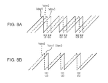
- FIGS. 8A and 8B are diagrams illustrating the waveforms of voltages according to a third exemplary embodiment.
- FIG. 8A illustrates the waveforms of voltages supplied in the case of “TC high” in FIG. 7
- FIG. 8B illustrates the waveforms of voltages supplied in the case of “TC low” in FIG. 7 .
- the voltage Vdev1 is a voltage supplied to the downstream roller 322 from the power supply 3291 .
- the voltage Vdev2 is a voltage supplied to the center roller 324 from the power supply 3292
- the voltage Vdev3 is a voltage supplied to the upstream roller 327 from a power supply 3293 .
- each of the three voltages Vdev1, Vdev2, and Vdev3 illustrated in FIG. 8A an AC voltage is superposed on a DC voltage.
- the AC components of the three voltages Vdev1, Vdev2, and Vdev3 are sawtooth waves having amplitudes and frequencies that are respectively the same as each other.
- the phases of the AC components are displaced from each other.
- t31 in which the voltage Vdev2 of the center roller 324 is higher than (has a negative value whose absolute value is smaller than) the voltage Vdev1 of the downstream roller 322 .
- the toner concentration of the developer distributed to the center roller 324 becomes higher than that of the developer distributed to the downstream roller 322 . Due to the presence of the periods t32, the toner concentration of the developer distributed to the upstream roller 327 becomes higher than that of the developer distributed to the center roller 324 . As a result, the toner concentration of the developer supported on the downstream roller 322 becomes the lowest.
- the phases of the voltages Vdev1 and Vdev3 illustrated in FIG. 8B are the same as each other and are displaced from the phase of the voltage Vdev2.
- the toner concentrations of the developer distributed to the upstream roller 327 and the downstream roller 322 become higher than that of the developer distributed to the center roller 324 .
- FIG. 9 is flowchart of an operation of an image forming apparatus according to the third exemplary embodiment.
- step S 34 The operation according to the third exemplary embodiment differs from that of the first exemplary embodiment illustrated in FIG. 4 in step S 34 , step S 36 , and step S 37 .
- Step S 34 in FIG. 9 is performed if the measured toner concentration is higher than the upper limit of the predetermined standard range (“Yes” in step S 13 ).
- step S 34 the toner concentration of the developer distributed to the downstream roller 322 is made the lowest.
- the controller 1 A illustrated in FIG. 6 causes the three power supplies 3291 , 3292 , and 3293 to respectively supply the voltages Vdev1, Vdev2, and Vdev3 having the waveforms illustrated in FIG. 8A . In this case, occurrence of toner fog due to excessively high toner concentration is reduced.
- Step S 36 is performed if the measured toner concentration is lower than the lower limit of the predetermined standard range (“Yes” in step S 15 ).
- the toner concentrations of the developer distributed to the upstream roller 327 and the downstream roller 322 are made higher than the developer distributed to the center roller 324 .
- the controller 1 A illustrated in FIG. 6 causes the three power supplies 3291 , 3292 , and 3293 to supply the voltages Vdev1, Vdev2, and Vdev3 having the waveforms illustrated in FIG. 8B . In this case, generation of a thin spot and decrease in the density of an image are reduced.
- Step S 37 is performed if the measured toner concentration is within the standard range (“No” in step S 15 ).
- the toner concentrations of the developer distributed to the upstream roller 327 , the center roller 324 , and the downstream roller 322 are made substantially the same.
- the controller 1 A illustrated in FIG. 6 causes the three power supplies 3291 , 3292 , and 3293 to supply the voltages Vdev1, Vdev2, and Vdev3 having substantially the same phase.
- the waveforms of voltages supplied to the upstream roller 327 , the center roller 324 , and the downstream roller 322 are rectangular wave, instead of the sawtooth waves.
- the difference between the fourth exemplary embodiment and the third exemplary embodiment will be described.
- FIGS. 10A and 10B are diagrams illustrating the waveforms of voltages supplied to the downstream roller, the center roller, and the upstream roller according to a fourth exemplary embodiment.
- FIG. 10A illustrates the waveforms of voltages supplied when in the case of “TC high” in FIG. 7
- FIG. 10B illustrates the waveforms of voltages supplied when in the case of “TC low” in FIG. 7 .
- the waveform of the voltage Vdev1 supplied to the downstream roller 322 and the waveform of the voltage Vdev3 supplied to the upstream roller 327 include pulses rising in opposite directions.
- the waveform of the voltage Vdev2 supplied to the center roller 324 includes positive pulses and negative pulses that alternately occur. That is, the pulses of the waveform of the voltage Vdev2 rise in a direction opposite to that of the pulses of the waveforms of the voltage Vdev1 and the voltage Vdev3.
- FIG. 10B illustrates the waveforms of the two voltages Vdev1 and Vdev3, which are the same as each other, and the waveform of the voltage Vdev2.
- Vdev1 and Vdev3 which are the same as each other
- Vdev2 the waveform of the voltage Vdev2.
- the toner concentration of the developer distributed to the upstream roller 327 becomes higher than that of the developer distributed to the center roller 324 .
- the toner concentration of the developer distributed to the downstream roller 322 becomes higher than that of the developer distributed to the center roller 324 .
- a sawtooth wave and a pulse wave are used as examples of a voltage waveform.
- the present invention is not limited to the exemplary embodiments, and the waveform may include, for example, curves having different rise and fall angles.
- the detector is the toner concentration sensor 28 , which detects the toner concentration in the container 21 .
- the present invention is not limited to the exemplary embodiments, and the detector may be a sensor that detects, for example, the toner concentration from the density of a reference image (batch image).
- two or three development rollers are used as examples of plural developer transport members.
- the present invention is not limited to the exemplary embodiments, and the number of the development rollers may be, for example, four or more.
- a tandem-type color printer is used as an example of an image forming apparatus.
- an image forming apparatus is not limited to this, and may be, for example, a monochrome printer that does not include an intermediate transfer belt.
- a photoconductor is used as an example of a latent image carrier.
- a latent image carrier is not limited to a photoconductor, and may be, for example, an object to which a voltage is directly applied by through an electrode.
Landscapes
- Physics & Mathematics (AREA)
- General Physics & Mathematics (AREA)
- Dry Development In Electrophotography (AREA)
- Control Or Security For Electrophotography (AREA)
- Developing For Electrophotography (AREA)
Abstract
Description
Claims (6)
Applications Claiming Priority (2)
| Application Number | Priority Date | Filing Date | Title |
|---|---|---|---|
| JP2012-185038 | 2012-08-24 | ||
| JP2012185038A JP5966770B2 (en) | 2012-08-24 | 2012-08-24 | Image forming apparatus |
Publications (2)
| Publication Number | Publication Date |
|---|---|
| US20140056603A1 US20140056603A1 (en) | 2014-02-27 |
| US8862005B2 true US8862005B2 (en) | 2014-10-14 |
Family
ID=50148074
Family Applications (1)
| Application Number | Title | Priority Date | Filing Date |
|---|---|---|---|
| US13/749,907 Active 2033-03-14 US8862005B2 (en) | 2012-08-24 | 2013-01-25 | Image forming apparatus |
Country Status (2)
| Country | Link |
|---|---|
| US (1) | US8862005B2 (en) |
| JP (1) | JP5966770B2 (en) |
Families Citing this family (6)
| Publication number | Priority date | Publication date | Assignee | Title |
|---|---|---|---|---|
| JP6451169B2 (en) * | 2014-09-18 | 2019-01-16 | 富士ゼロックス株式会社 | Powder coating apparatus, program, and powder coating method |
| JP6365212B2 (en) * | 2014-10-14 | 2018-08-01 | 京セラドキュメントソリューションズ株式会社 | Development device manufacturing method |
| JP6500456B2 (en) * | 2015-01-28 | 2019-04-17 | 富士ゼロックス株式会社 | Image forming device |
| JP6543992B2 (en) * | 2015-03-26 | 2019-07-17 | 富士ゼロックス株式会社 | Powder coating apparatus and powder coating method |
| JP2020052147A (en) * | 2018-09-25 | 2020-04-02 | 富士ゼロックス株式会社 | Image forming apparatus |
| JP7287021B2 (en) * | 2019-03-15 | 2023-06-06 | 富士フイルムビジネスイノベーション株式会社 | Developing device and image forming device |
Citations (4)
| Publication number | Priority date | Publication date | Assignee | Title |
|---|---|---|---|---|
| US5030996A (en) * | 1989-08-31 | 1991-07-09 | Canon Kabushiki Kaisha | Image forming apparatus with AC bias voltages for preventing developer mixture |
| JP2000098730A (en) | 1998-09-18 | 2000-04-07 | Fuji Xerox Co Ltd | Image forming device |
| US20100008692A1 (en) * | 2008-07-11 | 2010-01-14 | Samsung Electronics Co., Ltd. | Image forming apparatus and control method thereof |
| US20110299893A1 (en) * | 2010-06-08 | 2011-12-08 | Konica Minolta Business Technologies, Inc. | Developing device and developing method |
Family Cites Families (5)
| Publication number | Priority date | Publication date | Assignee | Title |
|---|---|---|---|---|
| JP5624279B2 (en) * | 2009-04-01 | 2014-11-12 | コニカミノルタ株式会社 | Development device |
| JP5458984B2 (en) * | 2010-03-15 | 2014-04-02 | 富士ゼロックス株式会社 | Developing device, assembly, and image forming apparatus |
| JP2011191664A (en) * | 2010-03-16 | 2011-09-29 | Ricoh Co Ltd | Image forming apparatus |
| JP5585142B2 (en) * | 2010-03-18 | 2014-09-10 | 富士ゼロックス株式会社 | Developing device and image forming apparatus |
| JP2012073572A (en) * | 2010-08-30 | 2012-04-12 | Ricoh Co Ltd | Developing device and image forming apparatus |
-
2012
- 2012-08-24 JP JP2012185038A patent/JP5966770B2/en not_active Expired - Fee Related
-
2013
- 2013-01-25 US US13/749,907 patent/US8862005B2/en active Active
Patent Citations (4)
| Publication number | Priority date | Publication date | Assignee | Title |
|---|---|---|---|---|
| US5030996A (en) * | 1989-08-31 | 1991-07-09 | Canon Kabushiki Kaisha | Image forming apparatus with AC bias voltages for preventing developer mixture |
| JP2000098730A (en) | 1998-09-18 | 2000-04-07 | Fuji Xerox Co Ltd | Image forming device |
| US20100008692A1 (en) * | 2008-07-11 | 2010-01-14 | Samsung Electronics Co., Ltd. | Image forming apparatus and control method thereof |
| US20110299893A1 (en) * | 2010-06-08 | 2011-12-08 | Konica Minolta Business Technologies, Inc. | Developing device and developing method |
Also Published As
| Publication number | Publication date |
|---|---|
| JP5966770B2 (en) | 2016-08-10 |
| JP2014044234A (en) | 2014-03-13 |
| US20140056603A1 (en) | 2014-02-27 |
Similar Documents
| Publication | Publication Date | Title |
|---|---|---|
| US8862005B2 (en) | Image forming apparatus | |
| CN102778831A (en) | Image forming apparatus | |
| US9829829B2 (en) | Developing device and image forming apparatus provided with same | |
| JP2010020281A (en) | Image forming apparatus | |
| JP2008287036A (en) | Developing method and device for image forming apparatus | |
| JP5820666B2 (en) | Image forming apparatus | |
| JP2016200619A (en) | Image forming apparatus | |
| JP2017219666A (en) | Image forming apparatus | |
| JP7604260B2 (en) | Image forming device | |
| US10423114B2 (en) | Power supply device, image forming apparatus, and output control method | |
| US20250053131A1 (en) | Image forming apparatus | |
| JP5255971B2 (en) | Developing device and image forming apparatus including the same | |
| JP2015203731A (en) | Developing device, process cartridge, and image forming apparatus | |
| JP5255972B2 (en) | Developing device and image forming apparatus including the same | |
| JP5264534B2 (en) | Image forming apparatus | |
| JP5847056B2 (en) | Image forming apparatus | |
| US9436118B2 (en) | Image forming apparatus for forming an image to change the potential of a photoconductor | |
| JP2014160222A (en) | Developing apparatus and image forming apparatus | |
| CN114167701B (en) | Image forming apparatus having a plurality of image forming units | |
| JP2015075729A (en) | Developing device and image forming apparatus having the same | |
| JP5193784B2 (en) | Developing device and image forming apparatus including the same | |
| JP4734358B2 (en) | Developing device and image forming apparatus | |
| JP2010243893A (en) | Developing device and image forming apparatus using the same | |
| JP2009244730A (en) | Development device and image forming apparatus having it | |
| JP2016090713A (en) | Developing device and image forming apparatus |
Legal Events
| Date | Code | Title | Description |
|---|---|---|---|
| AS | Assignment |
Owner name: FUJI XEROX CO., LTD., JAPAN Free format text: ASSIGNMENT OF ASSIGNORS INTEREST;ASSIGNORS:ABE, JUN;OBA, SHOTA;ONUKI, TOMIO;AND OTHERS;REEL/FRAME:029694/0393 Effective date: 20121210 |
|
| STCF | Information on status: patent grant |
Free format text: PATENTED CASE |
|
| MAFP | Maintenance fee payment |
Free format text: PAYMENT OF MAINTENANCE FEE, 4TH YEAR, LARGE ENTITY (ORIGINAL EVENT CODE: M1551) Year of fee payment: 4 |
|
| AS | Assignment |
Owner name: FUJIFILM BUSINESS INNOVATION CORP., JAPAN Free format text: CHANGE OF NAME;ASSIGNOR:FUJI XEROX CO., LTD.;REEL/FRAME:058287/0056 Effective date: 20210401 |
|
| MAFP | Maintenance fee payment |
Free format text: PAYMENT OF MAINTENANCE FEE, 8TH YEAR, LARGE ENTITY (ORIGINAL EVENT CODE: M1552); ENTITY STATUS OF PATENT OWNER: LARGE ENTITY Year of fee payment: 8 |