US8860216B1 - Method and system for providing a laser submount for an energy assisted magnetic recording head - Google Patents
Method and system for providing a laser submount for an energy assisted magnetic recording head Download PDFInfo
- Publication number
- US8860216B1 US8860216B1 US13/952,932 US201313952932A US8860216B1 US 8860216 B1 US8860216 B1 US 8860216B1 US 201313952932 A US201313952932 A US 201313952932A US 8860216 B1 US8860216 B1 US 8860216B1
- Authority
- US
- United States
- Prior art keywords
- submount
- facets
- silicon
- metallization
- laser diode
- Prior art date
- Legal status (The legal status is an assumption and is not a legal conclusion. Google has not performed a legal analysis and makes no representation as to the accuracy of the status listed.)
- Active
Links
- 238000000034 method Methods 0.000 title abstract description 21
- XUIMIQQOPSSXEZ-UHFFFAOYSA-N Silicon Chemical compound [Si] XUIMIQQOPSSXEZ-UHFFFAOYSA-N 0.000 claims abstract description 107
- 229910052710 silicon Inorganic materials 0.000 claims abstract description 107
- 239000010703 silicon Substances 0.000 claims abstract description 107
- 239000000758 substrate Substances 0.000 claims abstract description 74
- 229910000679 solder Inorganic materials 0.000 claims abstract description 37
- 239000002184 metal Substances 0.000 claims abstract description 10
- 229910052751 metal Inorganic materials 0.000 claims abstract description 10
- 239000004065 semiconductor Substances 0.000 claims 4
- 238000001465 metallisation Methods 0.000 abstract description 58
- 239000012212 insulator Substances 0.000 abstract description 9
- 238000000151 deposition Methods 0.000 description 15
- 229920002120 photoresistant polymer Polymers 0.000 description 13
- VYPSYNLAJGMNEJ-UHFFFAOYSA-N Silicium dioxide Chemical compound O=[Si]=O VYPSYNLAJGMNEJ-UHFFFAOYSA-N 0.000 description 12
- 238000004519 manufacturing process Methods 0.000 description 7
- 239000000463 material Substances 0.000 description 7
- 238000000206 photolithography Methods 0.000 description 6
- 235000012239 silicon dioxide Nutrition 0.000 description 6
- 239000000377 silicon dioxide Substances 0.000 description 6
- 230000004888 barrier function Effects 0.000 description 5
- 238000010586 diagram Methods 0.000 description 5
- 238000000227 grinding Methods 0.000 description 5
- 230000008569 process Effects 0.000 description 5
- 229910052581 Si3N4 Inorganic materials 0.000 description 4
- HQVNEWCFYHHQES-UHFFFAOYSA-N silicon nitride Chemical compound N12[Si]34N5[Si]62N3[Si]51N64 HQVNEWCFYHHQES-UHFFFAOYSA-N 0.000 description 4
- 229910052719 titanium Inorganic materials 0.000 description 4
- 230000008021 deposition Effects 0.000 description 3
- 229910052737 gold Inorganic materials 0.000 description 3
- 238000000059 patterning Methods 0.000 description 3
- 229910052697 platinum Inorganic materials 0.000 description 3
- 239000004593 Epoxy Substances 0.000 description 2
- 229910052804 chromium Inorganic materials 0.000 description 2
- 238000007796 conventional method Methods 0.000 description 2
- 229910052802 copper Inorganic materials 0.000 description 2
- 230000008878 coupling Effects 0.000 description 2
- 238000010168 coupling process Methods 0.000 description 2
- 238000005859 coupling reaction Methods 0.000 description 2
- 229910052738 indium Inorganic materials 0.000 description 2
- 238000000992 sputter etching Methods 0.000 description 2
- 239000000725 suspension Substances 0.000 description 2
- 229910052715 tantalum Inorganic materials 0.000 description 2
- 229910001218 Gallium arsenide Inorganic materials 0.000 description 1
- 239000000853 adhesive Substances 0.000 description 1
- 230000001070 adhesive effect Effects 0.000 description 1
- 230000002411 adverse Effects 0.000 description 1
- 229910045601 alloy Inorganic materials 0.000 description 1
- 239000000956 alloy Substances 0.000 description 1
- 229910052782 aluminium Inorganic materials 0.000 description 1
- 229910052787 antimony Inorganic materials 0.000 description 1
- 229910052797 bismuth Inorganic materials 0.000 description 1
- 230000008030 elimination Effects 0.000 description 1
- 238000003379 elimination reaction Methods 0.000 description 1
- 238000010438 heat treatment Methods 0.000 description 1
- 229910052745 lead Inorganic materials 0.000 description 1
- 229910052759 nickel Inorganic materials 0.000 description 1
- 229910052763 palladium Inorganic materials 0.000 description 1
- 230000009467 reduction Effects 0.000 description 1
- 229910052709 silver Inorganic materials 0.000 description 1
- -1 thermal tape Substances 0.000 description 1
- 229910052718 tin Inorganic materials 0.000 description 1
- 229910052721 tungsten Inorganic materials 0.000 description 1
Images


Classifications
-
- H—ELECTRICITY
- H01—ELECTRIC ELEMENTS
- H01L—SEMICONDUCTOR DEVICES NOT COVERED BY CLASS H10
- H01L23/00—Details of semiconductor or other solid state devices
- H01L23/48—Arrangements for conducting electric current to or from the solid state body in operation, e.g. leads, terminal arrangements ; Selection of materials therefor
- H01L23/488—Arrangements for conducting electric current to or from the solid state body in operation, e.g. leads, terminal arrangements ; Selection of materials therefor consisting of soldered or bonded constructions
- H01L23/498—Leads, i.e. metallisations or lead-frames on insulating substrates, e.g. chip carriers
- H01L23/49811—Additional leads joined to the metallisation on the insulating substrate, e.g. pins, bumps, wires, flat leads
-
- G—PHYSICS
- G11—INFORMATION STORAGE
- G11B—INFORMATION STORAGE BASED ON RELATIVE MOVEMENT BETWEEN RECORD CARRIER AND TRANSDUCER
- G11B5/00—Recording by magnetisation or demagnetisation of a record carrier; Reproducing by magnetic means; Record carriers therefor
- G11B5/127—Structure or manufacture of heads, e.g. inductive
- G11B5/31—Structure or manufacture of heads, e.g. inductive using thin films
- G11B5/3109—Details
- G11B5/313—Disposition of layers
- G11B5/3133—Disposition of layers including layers not usually being a part of the electromagnetic transducer structure and providing additional features, e.g. for improving heat radiation, reduction of power dissipation, adaptations for measurement or indication of gap depth or other properties of the structure
- G11B5/314—Disposition of layers including layers not usually being a part of the electromagnetic transducer structure and providing additional features, e.g. for improving heat radiation, reduction of power dissipation, adaptations for measurement or indication of gap depth or other properties of the structure where the layers are extra layers normally not provided in the transducing structure, e.g. optical layers
-
- B—PERFORMING OPERATIONS; TRANSPORTING
- B23—MACHINE TOOLS; METAL-WORKING NOT OTHERWISE PROVIDED FOR
- B23K—SOLDERING OR UNSOLDERING; WELDING; CLADDING OR PLATING BY SOLDERING OR WELDING; CUTTING BY APPLYING HEAT LOCALLY, e.g. FLAME CUTTING; WORKING BY LASER BEAM
- B23K26/00—Working by laser beam, e.g. welding, cutting or boring
- B23K26/36—Removing material
- B23K26/362—Laser etching
- B23K26/364—Laser etching for making a groove or trench, e.g. for scribing a break initiation groove
-
- B—PERFORMING OPERATIONS; TRANSPORTING
- B23—MACHINE TOOLS; METAL-WORKING NOT OTHERWISE PROVIDED FOR
- B23K—SOLDERING OR UNSOLDERING; WELDING; CLADDING OR PLATING BY SOLDERING OR WELDING; CUTTING BY APPLYING HEAT LOCALLY, e.g. FLAME CUTTING; WORKING BY LASER BEAM
- B23K26/00—Working by laser beam, e.g. welding, cutting or boring
- B23K26/36—Removing material
- B23K26/40—Removing material taking account of the properties of the material involved
-
- G—PHYSICS
- G11—INFORMATION STORAGE
- G11B—INFORMATION STORAGE BASED ON RELATIVE MOVEMENT BETWEEN RECORD CARRIER AND TRANSDUCER
- G11B7/00—Recording or reproducing by optical means, e.g. recording using a thermal beam of optical radiation by modifying optical properties or the physical structure, reproducing using an optical beam at lower power by sensing optical properties; Record carriers therefor
- G11B7/12—Heads, e.g. forming of the optical beam spot or modulation of the optical beam
-
- B—PERFORMING OPERATIONS; TRANSPORTING
- B23—MACHINE TOOLS; METAL-WORKING NOT OTHERWISE PROVIDED FOR
- B23K—SOLDERING OR UNSOLDERING; WELDING; CLADDING OR PLATING BY SOLDERING OR WELDING; CUTTING BY APPLYING HEAT LOCALLY, e.g. FLAME CUTTING; WORKING BY LASER BEAM
- B23K2103/00—Materials to be soldered, welded or cut
- B23K2103/50—Inorganic material, e.g. metals, not provided for in B23K2103/02 – B23K2103/26
-
- G—PHYSICS
- G11—INFORMATION STORAGE
- G11B—INFORMATION STORAGE BASED ON RELATIVE MOVEMENT BETWEEN RECORD CARRIER AND TRANSDUCER
- G11B5/00—Recording by magnetisation or demagnetisation of a record carrier; Reproducing by magnetic means; Record carriers therefor
- G11B2005/0002—Special dispositions or recording techniques
- G11B2005/0005—Arrangements, methods or circuits
- G11B2005/0021—Thermally assisted recording using an auxiliary energy source for heating the recording layer locally to assist the magnetization reversal
-
- H—ELECTRICITY
- H01—ELECTRIC ELEMENTS
- H01L—SEMICONDUCTOR DEVICES NOT COVERED BY CLASS H10
- H01L2924/00—Indexing scheme for arrangements or methods for connecting or disconnecting semiconductor or solid-state bodies as covered by H01L24/00
- H01L2924/0001—Technical content checked by a classifier
- H01L2924/0002—Not covered by any one of groups H01L24/00, H01L24/00 and H01L2224/00
Definitions
- FIG. 1 depicts a side view of portion of a conventional energy assisted magnetic recording (EAMR) disk drive 10 .
- the conventional EAMR disk drive 10 includes a recording media 12 , a conventional slider 20 , and a conventional laser diode 30 that are typically attached to a suspension (not shown).
- the conventional slider 20 has a leading edge 22 , a trailing edge 26 , and a back side 24 . Although termed “edges”, the leading edge 22 and trailing edge 26 are surfaces of the slider 20 . The leading edge 22 and trailing edge 26 are so termed because of the direction the conventional media 12 travels with respect to the EAMR transducer 28 . Other components that may be part of the conventional EAMR disk drive 10 are not shown.
- the conventional slider 20 is typically attached to the suspension at its back side 24 .
- a conventional EAMR transducer 28 is coupled with the slider 20 .
- the laser diode 30 is typically mounted on a conventional submount 32 .
- the laser diode 30 and conventional submount 32 are coupled in proximity to the EAMR transducer 28 on the back side 24 of the slider 20 .
- the conventional submount 32 is typically SiC, which is a high thermal conductivity insulator. The conventional submount may thus act as a heat sink for the laser diode 30 .
- the conventional submount 32 may also have bond pads (not shown) and electrical traces (not shown). Thus, the conventional submount 32 is typically also desired to provide electrical and thermal connection as well as mechanical support to the laser diode 30 .
- light from the conventional laser diode 30 is provided to the EAMR transducer 28 . More specifically, light from the laser diode 30 is provided to a waveguide (not shown) of conventional EAMR transducer 28 .
- the waveguide directs the light toward the conventional media 12 , heating a small region of the conventional media 12 .
- the conventional EAMR transducer 28 magnetically writes to the conventional media 12 in the region the conventional media 12 is heated.
- FIG. 2 depicts a conventional method 50 for mounting the laser diode 20 on the conventional EAMR disk drive 10 .
- the conventional submount 32 is prepared from a SiC substrate. Electrical traces for the submounts on the SiC substrate are provided, via step 52 .
- the SiC substrate is lapped to reduce the thickness of the substrate, via step 54 .
- the SiC substrate is then diced into the individual conventional submounts 32 , via step 56 .
- the faces of the substrate correspond to the faces of the submount to which the laser diode 30 is coupled.
- the laser 30 is affixed to the submount, via step 58 .
- the laser diode 30 and conventional submount 32 are then mounted to the slider 20 , via step 60 . Fabrication of the conventional EAMR disk drive 10 may then be completed.
- the conventional EAMR disk drive 10 and method 50 may function, improvements are desired. More specifically, properly aligning and coupling the laser diode 30 to the slider 20 and conventional submount 32 may be problematic.
- the sidewalls of the conventional submount 32 may be rough and chipped due to dicing.
- proper alignment of the conventional submount 32 to the slider 20 may be challenging. This may affect alignment of the laser diode 30 , which is affixed to the conventional submount 32 .
- the laser diode 30 may be tilted from vertical or otherwise misaligned as is shown in FIG. 1 .
- the lapped surface of the conventional submount 32 may also be rounded, which is undesirable.
- the back surface of the conventional submount 32 shows such rounding in FIG. 1 .
- the electrical traces on the submount 32 may be misaligned.
- proper alignment of the laser diode 30 may be challenging. Such misalignments may adversely affect performance of the conventional EAMR disk drive 10 .
- a method and system for providing a laser diode submount for use in an EAMR disk drive is described.
- a portion of a silicon substrate is removed to form trenches therein.
- the trenches have sidewalls and surround silicon islands corresponding to a laser diode submounts.
- Each of the trenches corresponds to a thickness of the laser diode submount.
- the silicon island has a top surface and a plurality of facets corresponding to the sidewalls of the plurality of trenches. At least one insulator for the top surface and the plurality of facets of the silicon island is provided.
- Metallization is provided on the top surface and the facets of the silicon island.
- a first portion of the metallization on the top surface corresponds to under bump metal (UBM) for at least one solder pad.
- a second portion of the metallization corresponds to electrical traces. At least one solder pad is provided on the UBM on the top surface of the silicon island. The silicon island is released from the silicon substrate.
- UBM under bump metal
- FIG. 1 is a diagram depicting a portion of a conventional energy assisted magnetic recording disk drive.
- FIG. 2 is a flow chart depicting a conventional method for fabricating a conventional EAMR disk drive.
- FIG. 3 is a flow chart depicting an exemplary embodiment of a method for fabricating a laser submount usable in an EAMR disk drive.
- FIG. 4 is a diagram depicting an exemplary embodiment of a submount.
- FIG. 5 is a flow chart depicting another exemplary embodiment of a method for fabricating a laser submount usable in an EAMR disk drive.
- FIG. 6A-6B are diagrams depicting an exemplary embodiment of an EAMR head during fabrication.
- FIGS. 7A-21 are diagrams depicting an exemplary embodiment of an EAMR head during fabrication.
- FIG. 3 is a flow chart depicting an exemplary embodiment of a method 100 for a laser submount that may be used in conjunction with EAMR heads. Although certain steps are shown, some steps may be omitted, interleaved, performed in another order, and/or combined. Further, although described in the context of mounting a laser for an EAMR head, in other embodiments, the submount may be used for other purposes.
- the EAMR heads may be merged heads, each of which includes an EAMR write transducer, a read transducer (not shown) and resides on a slider.
- the method commences with a silicon substrate.
- the silicon substrate has a high thermal conductivity.
- a portion of a silicon substrate is removed, via step 102 .
- step 102 include performing a silicon reactive ion etch (RIE), such as a deep RIE.
- Step 102 may include forming a hard mask having apertures corresponding to the trenches. Stated differently, the size, shape, and location of the apertures correspond to the trench size, shape, and location.
- the hard mask may be formed by depositing a hard mask layer, providing a photoresist mask on the hard mask layer using photolithography, and transferring the pattern of the photoresist mask to the hard mask layer. In other embodiments, the mask may be other than a hard mask and/or be formed in another manner.
- the hard mask may include silicon dioxide, silicon nitride, Ti, Ta, and/or Ni. However, in other embodiments, other materials may be used.
- the silicon RIE then removes the silicon exposed by the apertures. Thus, trenches are formed in the silicon substrate.
- Each trench corresponds to one or more silicon island.
- the trenches can be considered to surround silicon islands.
- a single trench surrounds a single silicon island.
- trenches may combine to define one or more silicon islands.
- Trenches correspond to a thickness of the laser diode submount.
- the depth of the trench is a desired thickness for the laser diode submount.
- the trenches are at least fifty microns deep.
- the trenches are at least one hundred microns deep.
- the trenches are at one hundred fifty microns deep.
- the trenches may be at least two hundred microns deep, depending upon the desired thickness for the submount.
- the silicon islands formed in step 102 have top surfaces and facets (side faces) corresponding to the sidewalls of the trenches. Each silicon island corresponds to a laser submount. A single laser submount may be used for mounting one or more laser diodes.
- the top surface and facets form well controlled angles. In some embodiments, these angles are right angles. In some embodiments, the angles formed by the top surface and facets are at least 89.5 degrees and not more than 90.5 degrees.
- At least one insulator is provided for the top surface and the facets of the silicon island, via step 104 . In some embodiments, this includes forming insulator(s) on all surfaces of the silicon substrate, including the trench bottoms. In some embodiments, an insulating layer is deposited on the silicon substrate. In other embodiments, the insulating layer may be grown. The insulating layer may include materials such as silicon dioxide and silicon nitride.
- Metallization is provided on the top surface and the plurality of facets of the silicon island, via step 106 .
- a first portion of the metallization on the top surface of the islands corresponds to under bump metal (UBM) for solder pad(s).
- a second portion of the metallization corresponds to electrical traces. Because the metallization is provided on both the top surfaces and the facets of the silicon islands, the solder pads and electrical traces may be on the top surfaces and/or the facets of the silicon islands.
- Step 106 may include providing a mask having apertures corresponding to the locations of the electrical traces and UBM.
- the metallization may then be deposited. After deposition, the metallization mask may be removed. Deposition of the metallization may include depositing multiple layers.
- step 106 generally includes blanket depositing multiple layers for at least the UBM.
- an adhesion layer, a barrier layer and a top metal layer may be deposited.
- the adhesion layer assists ensuring that subsequent layers, including the solder pad(s), adhere to the silicon.
- the adhesion layer may include one or more of Ti, Cr, and Ta.
- the barrier layer aids in ensuring that the adhesion layer is not melted or otherwise disturbed by the use of the solder and the processing temperatures required.
- the barrier layer includes at least one of Pt, Ni, Pd, and W.
- the top metal layer may include materials such as Au, Al and/or Cu.
- the same metallization may be used for the UBM and for the electrical traces. However, in other embodiments, different masks and/or different metallization may be used for the UBM and the electrical traces.
- At least one solder pad is provided on the UBM on the top surfaces of the silicon islands, via step 108 .
- solder pads may also be provided on the UBM on the desired facets of the silicon island.
- Step 108 may be performed by providing a mask having apertures corresponding to the desired locations of the solder pads and depositing solder pads. The mask may then be removed.
- Step 110 may include temporarily mounting the silicon substrate to a carrier substrate top side down.
- the surface of the silicon substrate in which the trenches and silicon islands are formed is bonded to the carrier substrate.
- Temporary adhesive such as thermal tape, epoxy, and/or wax might be used to bond the silicon substrate to the carrier substrate.
- the silicon substrate is then thinned from the back side.
- the silicon substrate may be ground down. The grinding ceases before the trenches in the silicon substrate have been exposed. In some embodiments, grinding ceases a distance of at least ten microns from the bottom of the trench. In other embodiments, the grinding is terminated when the exposed surface of the silicon is at least twenty microns from the bottom of the trench.
- a silicon substrate having a total thickness of seven hundred microns and a trench depth of two hundred microns might have approximately four hundred ninety microns of silicon removed from the backside by grinding.
- the silicon substrate may then be etched to the trench bottom.
- a silicon RIE might be used.
- a wet etch might be employed.
- the silicon substrate is removed to the bottom of the trench.
- only the insulating layer and/or the metallization connect the islands to the remaining portion of the silicon substrate.
- the insulating layer and metallization may then be removed, for example via appropriate ion milling.
- no additional materials reside at the trench bottom.
- removal of the silicon substrate separates the silicon islands.
- the silicon islands are no longer connected to the remaining portions of the substrate.
- the silicon islands may then be released from the carrier substrate.
- individual laser diode submounts have been formed.
- FIGS. 4A and 4B depict top and side views, respectively, of an exemplary embodiment of a laser submount 150 fabricated using the method 100 .
- the substrate 152 for the laser submount 150 is a silicon substrate.
- the submount 150 has a thickness, t, of not more than two hundred microns thick. In other embodiments, the submount 150 is not more than one hundred and fifty microns thick.
- the silicon island has been separated from the remaining silicon substrate by trenches (not shown) and the process described above and used to form the submount 150 . Also shown are insulating layer 154 , metallization 156 and solder pads 158 .
- the metallization 156 also underlies the solder pads 158 .
- the insulator 154 underlies the metallization 156 .
- some structures are labeled 154 / 156 / 158 to indicate the presence of multiple layers.
- laser submount 150 may be fabricated. As can be seen in FIG. 4B , the angle, ⁇ , between the facet (side) of the submount 150 and the top surface is well controlled and in the embodiment shown, approximately ninety degrees. This is because as a removal process such as an RIE was used to define the silicon islands. The RIE also results in reduction or elimination of chipping and analogous issues with the sidewalls. Consequently, alignment of the laser (not shown) to a slider (not shown) may be improved.
- metallization 156 may be provided on the top surface and facets of the laser submount. Because of the insulating layer 154 , the metallization is not shorted through the silicon substrate. Further, solder pads 158 have been formed.
- solder pads may also be provided on the facets of the laser submount 150 . Because wafer level photolithography is used in providing the metallization/UBM 156 and the solder pads 158 , the alignment of the electrical traces and solder pads so formed may be improved. Furthermore, the silicon substrate 152 has a relatively high thermal conductivity while being electrically insulated by insulator 154 . Thus, heat management of the laser can be provided while allowing for electrical connection to be made to desired portions of the slider and laser. As such, fabrication of an EAMR head or other device using a laser, as well as performance of the EAMR head or other device may be improved.
- FIG. 5 is a flow chart depicting another exemplary embodiment of a method 200 for fabricating a laser submount.
- FIGS. 6A-20B are diagrams depicting portions of a laser submount during fabrication. For clarity, FIGS. 6A-20B are not to scale. Further, for simplicity, not all components are labeled in FIGS. 6A-20B .
- the laser submount 250 being fabricated may be used in connection with an EAMR head and reside on a slider of a disk drive. However, the laser submount may be used in another device.
- the method 200 is described in the context of a single laser submount depicted in FIGS. 6A-20B , multiple laser submounts are typically fabricated in parallel.
- the laser submount depicted in FIGS. 6A-20B may be used to mount a laser diode, such as a GaAs laser diode.
- a laser diode such as a GaAs laser diode.
- other lasers, other diodes, and/or other components may be mounted on the submount.
- a hard mask is first formed on a silicon substrate in steps 202 - 206 .
- a hard mask layer is deposited on the silicon substrate, via step 202 .
- the hard mask layer consists of silicon dioxide.
- the hard mask may include or consist of other materials such as silicon nitride.
- the silicon substrate has a top surface and a back surface opposite to the top surface.
- the hard mask layer is on the top surface of the substrate.
- FIGS. 6A and 6B depict top and side views of the laser submount 250 after step 202 has been performed.
- a silicon substrate 252 having a hard mask layer 254 deposited on the top is shown.
- step 204 includes depositing a photoresist layer and patterning the photoresist layer using photolithography.
- FIGS. 7A and 7B depict top and side views of the submount 250 after step 204 is performed. Thus, a mask 256 having aperture 258 is shown.
- the pattern of the photoresist mask 256 is transferred to the hard mask layer, via step 206 .
- a RIE or other etch process appropriate to the hard mask is used.
- the photoresist mask may also be stripped as part of step 206 .
- a hard mask having apertures corresponding to the pattern is formed.
- FIGS. 8A and 8B depict top and side views of the submount 250 after step 206 is performed.
- the apertures 258 ′ have thus been transferred to the hard mask 254 ′.
- the underlying portion of the silicon substrate 252 is exposed.
- a deep silicon RIE is performed, via step 208 .
- the silicon RIE removes a portion of the silicon substrate 252 exposed by apertures 258 ′. Trenches are thus formed in the silicon substrate 252 .
- FIGS. 9A and 9B depict top and side views of the submount 250 after step 208 is performed. Trenches 260 have been formed in the silicon substrate. Each of the trenches 260 surrounding a silicon island 261 corresponding to a laser diode submount being formed. Each trench 260 has a trench bottom, sidewalls, and a depth, d. The depth corresponds to a desired thickness for the laser diode submount 250 . The depth is at least one hundred microns. In some embodiments, the depth is at least two hundred microns.
- the trench may be wide.
- the trenches 260 are at least one hundred microns and not more than one hundred fifty microns wide. However, other widths may be used.
- a typical silicon substrate 252 is approximately seven hundred microns thick. Thus, the depth of the trenches 260 is less than seven hundred microns (e.g. less than the depth of the silicon substrate). This is because the silicon islands 21 are desired to remain attached to the substrate 252 during fabrication.
- the silicon island 261 has a top face (shown in FIG. 9A ) and facets corresponding to the sidewalls of the trenches 260 . In some embodiments, the top face of the silicon island 261 measures approximately 400 microns by 700 microns. However, in other embodiments, the dimensions may differ.
- the dimensions may be 350 microns by 400 microns.
- the top face and the facets forming a top angle, ⁇ , of at least 89.5 degrees and not more than 90.5 degrees.
- the same angle, ⁇ is shown at multiple facets.
- different facets may make different angles with the top surface of the silicon island 261 . However, in some embodiments, all of these angles are within 0.5 degree of ninety degrees.
- the hard mask 254 ′ is removed, via step 210 .
- a solution such as buffered HF may be used to remove the hard mask.
- Step 212 may include depositing or growing the insulating layer.
- the insulating layer may be silicon dioxide, silicon nitride, or some other insulator on the top face and the facets of the silicon island 261 .
- the insulating layer 262 is used to electrically insulate the silicon substrate 252 from the metallization, described below.
- a metallization mask is provided, via step 214 .
- Step 214 may include depositing a photoresist layer and patterning the photoresist layer using photolithography.
- the metallization mask has a metallization mask pattern. This pattern includes one or more apertures for the metallization to be provided. The apertures thus correspond to one under bump metal (UBM) to be provided on the top surface and/or facets of the silicon island 261 and for electrical traces for the silicon island 261 .
- FIGS. 11A and 11B depict top and side views of the submount 250 after step 214 is performed.
- a metallization mask 264 has been provided.
- the metallization mask 264 only exposes regions in which the metallization is desired.
- part of the metallization mask 264 resides in and covers portions of the trenches 260 .
- the metallization layer(s) are deposited, via step 216 .
- the metallization is blanket deposited.
- Deposition of the metallization layer(s) in step 216 may include depositing an adhesion layer, depositing a barrier layer, and depositing an additional metal layer. These layers may be desirable for use as the UBM for solder pads.
- the portion of the metallization layer(s) to be used as UBM is fabricated at substantially the same time as the layers for the electrical traces. Thus, the same materials (including adhesion, barrier, and metal layers) may be used for both. Processing may thus be simplified.
- the metallization for the electrical traces may be provided separately from the metallization for the UBM.
- FIGS. 12A and 12B depict top and side views of the submount 250 after step 216 is performed. Some underlying features are denoted in the top view by dashed or dotted lines. The metallization 266 is thus shown. Portions of the metallization are on the metallization mask 264 .
- Step 218 may include stripping the photoresist metallization mask 264 .
- a solder pad mask is provided, via step 220 .
- Step 220 may include depositing a photoresist layer and patterning the photoresist layer using photolithography.
- the solder pad mask has solder pad mask pattern. This pattern includes apertures corresponding to the size, shape, and location of the desired solder pads.
- FIGS. 14A and 14B depict side and top views of the submount 250 after step 220 is performed. Some underlying features are denoted in the top view by dashed or dotted lines.
- a solder bond pad mask 268 is shown. Some underlying features are denoted in the top view by dashed or dotted lines.
- the mask 268 includes apertures 270 therein. The apertures 270 expose the underlying metallization 266 ′.
- step 222 includes depositing at least one of Ti, In, Pt, Au, Sn, In, Pb, Bi, Sb, Cu, Ag, and their alloys.
- solder pad mask is removed, via step 224 .
- solder pads have been provided in steps 220 - 224 .
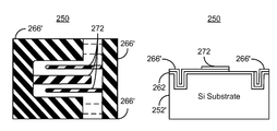
- FIGS. 15A and 15B depict top and side views, respectively, of the submount 250 after step 224 is performed.
- Solder pads 272 have been deposited on a portion of the metallization 266 ′. This portion of the metallization 266 ′ may be considered to be UBM for these solder pads 272 .
- the silicon islands 261 are then separated from the silicon substrate 252 , using step 226 - 236 .
- the top surface of the silicon substrate 252 ′ is temporarily bonded to a carrier substrate, via step 226 .
- the silicon islands face the carrier substrate.
- the temporary bond formed in step 226 may be carried out using wax, photoresist, temporary epoxy, and/or thermal tape.
- FIG. 16 depicts a side view of the laser submount 250 after step 226 is performed.
- the silicon substrate 252 ′ is attached to carrier substrate 274 through temporary bond 276 .
- step 228 is preformed through grinding and/or lapping.
- the silicon substrate 252 ′ is thinned.
- FIGS. 17A and 17B depict back side and side views of submount 250 after step 228 is performed.
- the silicon substrate 252 ′′ has been thinned.
- An interior surface of the silicon substrate 252 ′′ has been exposed. This surface is a small distance from the trench bottom (shown as dashed lines in FIG. 17A ). In some embodiments this distance is not more than twenty microns. In some such embodiments, the distance is not more than ten microns.
- step 230 is performed using a silicon RIE. In other embodiments, a Si wet etch may be used. Because a silicon removal process is used, the removal process stops at the insulating layer 262 or the metallization layer(s) 266 ′.
- Step 232 A portion of insulating layer is removed, via step 232 .
- Step 232 may be performed using a silicon dioxide RIE or ion milling.
- a portion of metallization layer(s) 266 ′ on the trench bottom are exposed.
- the exposed portion of the metallization layer(s) is also removed, via step 234 .
- step 234 is performed using an ion mill.
- FIGS. 19A and 19B depict backside and side views of the submount 250 after step 232 is performed.
- the temporary bond 276 may be exposed. The islands 261 are held together only by the temporary bond 276 .
- FIGS. 20A and 20B depict the submount 250 after step 236 is performed.
- metallization 266 ′′ and solder pads 272 have been provided on a silicon island 261 having an insulating layer 262 ′.
- FIG. 21 depicts one use of the submount 250 .
- FIG. 21 depicts an EAMR disk drive 300 including media 312 , slider 320 having leading edge 322 , trailing edge 326 and back side 324 .
- an EAMR transducer 328 and layers 332 are also shown.
- the submount 250 formed using the method 200 is also shown.
- the laser diode 332 has been affixed to the submount 250 and the combination mounted on the slider 320 .
- the submount 250 may be formed.
- the submount 250 shares the benefits of the submount 150 .
- the angle, ⁇ , between the facet (side) of the submount 150 and the top surface is approximately ninety degrees. Chipping and analogous issues with the sidewalls may also be mitigated or eliminated. Consequently, alignment of the laser 332 to the slider 250 may be improved.
- metallization 266 ′′ may be provided on the top surface and facets of the laser submount. Because of the insulating layer 262 ′, the metallization is not shorted through the silicon island 261 . Further, solder pads 272 have been formed.
- solder pads may also be provided on the facets of the laser submount 250 . Because wafer level photolithography is used in providing the metallization/UBM 266 ′′ and the solder pads 272 , the alignment of the electrical traces and solder pads so formed may be improved. Furthermore, the silicon island 261 has a relatively high thermal conductivity while being electrically insulated by insulator 262 ′. Thus, heat management of the laser 332 can be provided while allowing for electrical connection to be made to desired portions of the slider 320 and laser 332 . As such, fabrication of an EAMR head 300 or other device using a laser as well as performance of the EAMR head or other device may be improved.
Landscapes
- Engineering & Computer Science (AREA)
- Physics & Mathematics (AREA)
- Optics & Photonics (AREA)
- Mechanical Engineering (AREA)
- Plasma & Fusion (AREA)
- Manufacturing & Machinery (AREA)
- Electromagnetism (AREA)
- Computer Hardware Design (AREA)
- Microelectronics & Electronic Packaging (AREA)
- Power Engineering (AREA)
- General Physics & Mathematics (AREA)
- Condensed Matter Physics & Semiconductors (AREA)
- Semiconductor Lasers (AREA)
Abstract
Description
Claims (3)
Priority Applications (1)
| Application Number | Priority Date | Filing Date | Title |
|---|---|---|---|
| US13/952,932 US8860216B1 (en) | 2011-06-29 | 2013-07-29 | Method and system for providing a laser submount for an energy assisted magnetic recording head |
Applications Claiming Priority (2)
| Application Number | Priority Date | Filing Date | Title |
|---|---|---|---|
| US13/172,583 US8518748B1 (en) | 2011-06-29 | 2011-06-29 | Method and system for providing a laser submount for an energy assisted magnetic recording head |
| US13/952,932 US8860216B1 (en) | 2011-06-29 | 2013-07-29 | Method and system for providing a laser submount for an energy assisted magnetic recording head |
Related Parent Applications (1)
| Application Number | Title | Priority Date | Filing Date |
|---|---|---|---|
| US13/172,583 Division US8518748B1 (en) | 2011-06-29 | 2011-06-29 | Method and system for providing a laser submount for an energy assisted magnetic recording head |
Publications (1)
| Publication Number | Publication Date |
|---|---|
| US8860216B1 true US8860216B1 (en) | 2014-10-14 |
Family
ID=48999710
Family Applications (2)
| Application Number | Title | Priority Date | Filing Date |
|---|---|---|---|
| US13/172,583 Active US8518748B1 (en) | 2011-06-29 | 2011-06-29 | Method and system for providing a laser submount for an energy assisted magnetic recording head |
| US13/952,932 Active US8860216B1 (en) | 2011-06-29 | 2013-07-29 | Method and system for providing a laser submount for an energy assisted magnetic recording head |
Family Applications Before (1)
| Application Number | Title | Priority Date | Filing Date |
|---|---|---|---|
| US13/172,583 Active US8518748B1 (en) | 2011-06-29 | 2011-06-29 | Method and system for providing a laser submount for an energy assisted magnetic recording head |
Country Status (1)
| Country | Link |
|---|---|
| US (2) | US8518748B1 (en) |
Families Citing this family (6)
| Publication number | Priority date | Publication date | Assignee | Title |
|---|---|---|---|---|
| US8518279B1 (en) * | 2010-11-15 | 2013-08-27 | Western Digital (Fremont), Llc | Method and system for providing a laser cavity for an energy assisted magnetic recording head |
| US8518748B1 (en) | 2011-06-29 | 2013-08-27 | Western Digital (Fremont), Llc | Method and system for providing a laser submount for an energy assisted magnetic recording head |
| US9202754B2 (en) * | 2012-04-23 | 2015-12-01 | Seagate Technology Llc | Laser submounts formed using etching process |
| US20130277863A1 (en) * | 2012-04-23 | 2013-10-24 | Seagate Technology Llc | Solderable pad fabrication for microelectronic components |
| US9361916B1 (en) | 2014-03-13 | 2016-06-07 | Western Digital (Fremont) | Electrical lapping guide for dimensional control of back side of heat assisted magnetic recording device |
| US9025423B1 (en) * | 2014-07-14 | 2015-05-05 | HGST Netherlands B.V. | Thermally conductive features for a heat-assisted magnetic recording head |
Citations (44)
| Publication number | Priority date | Publication date | Assignee | Title |
|---|---|---|---|---|
| US5478781A (en) * | 1993-06-21 | 1995-12-26 | International Business Machines Corporation | Polyimide-insulated cube package of stacked semiconductor device chips |
| US5687267A (en) | 1994-09-28 | 1997-11-11 | Optobahn Corporation | Integrated optoelectronic coupling and connector |
| US5700732A (en) * | 1996-08-02 | 1997-12-23 | Micron Technology, Inc. | Semiconductor wafer, wafer alignment patterns and method of forming wafer alignment patterns |
| US5907571A (en) | 1996-05-22 | 1999-05-25 | Fuji Electric Co., Ltd. | Semiconductor laser device and method for manufacturing the same |
| US6164837A (en) | 1998-12-30 | 2000-12-26 | Mcdonnell Douglas Corporation | Integrated microelectromechanical alignment and locking apparatus and method for fiber optic module manufacturing |
| US20020089913A1 (en) | 2000-07-21 | 2002-07-11 | Katsuya Moriyama | Light source device for an optical head apparatus and method relating thereto |
| US20020163865A1 (en) | 2001-05-01 | 2002-11-07 | Zimmer Erik J. | Optical pickup unit assembly process |
| US6485198B1 (en) | 2001-12-12 | 2002-11-26 | Industrial Technology Research Institute | Optoelectronic transceiver having integrated optical and electronic components |
| US20030002549A1 (en) | 2000-05-24 | 2003-01-02 | Oh Myeong Seok | Two-wavelength laser diode, and manufacturing method therefor |
| US6534794B1 (en) | 1999-08-05 | 2003-03-18 | Matsushita Electric Industrial Co., Ltd. | Semiconductor light-emitting unit, optical apparatus and optical disk system having heat sinking means and a heating element incorporated with the mounting system |
| US6577656B2 (en) | 2001-03-13 | 2003-06-10 | Finisar Corporation | System and method of packaging a laser/detector |
| US6627096B2 (en) | 2000-05-02 | 2003-09-30 | Shipley Company, L.L.C. | Single mask technique for making positive and negative micromachined features on a substrate |
| US6804276B2 (en) | 2000-09-19 | 2004-10-12 | Kabushiki Kaisha Toshiba | Semiconductor laser device which removes influences from returning light of three beams and a method of manufacturing the same |
| US6811853B1 (en) | 2000-03-06 | 2004-11-02 | Shipley Company, L.L.C. | Single mask lithographic process for patterning multiple types of surface features |
| US20040231997A1 (en) | 2001-11-07 | 2004-11-25 | Xinming Wang | Substrate processing apparatus and method |
| US6858871B2 (en) | 2000-12-25 | 2005-02-22 | Sharp Kabushiki Kaisha | Semiconductor device and manufacturing method therefor |
| US6960485B2 (en) | 2000-03-31 | 2005-11-01 | Toyoda Gosei Co., Ltd. | Light-emitting device using a group III nitride compound semiconductor and a method of manufacture |
| US20070015313A1 (en) | 2003-03-08 | 2007-01-18 | Samsung Electronics Co., Ltd. | Submount of semiconductor laser diode, method of manufacturing the same, and semiconductor laser diode assembly using the submount |
| US7217955B2 (en) | 2003-10-21 | 2007-05-15 | Sharp Kabushiki Kaisha | Semiconductor laser device |
| US20080056073A1 (en) | 2006-08-30 | 2008-03-06 | Junichiro Shimizu | Recording head |
| US7371017B1 (en) | 2003-11-10 | 2008-05-13 | Finisar Corporation | Automated laser pressing system |
| US7449905B2 (en) | 2006-02-13 | 2008-11-11 | Finisar Corporation | Automated characterization system for laser chip on a submount |
| US20080316872A1 (en) | 2007-06-21 | 2008-12-25 | Junichiro Shimizu | Optical device integrated head |
| US20090035885A1 (en) | 2007-05-30 | 2009-02-05 | Luminus Devices, Inc. | Methods of forming light-emitting structures |
| US7502397B2 (en) | 2002-12-26 | 2009-03-10 | Sony Corporation | Semiconductor laser assembly |
| US7522649B2 (en) | 2006-06-08 | 2009-04-21 | Samsung Electronic, Co., Ltd | Submount of a multi-beam laser diode module |
| US20090207580A1 (en) | 2005-03-18 | 2009-08-20 | Yoshikazu Oshika | Submount and Method of Manufacturing the Same |
| US20090219728A1 (en) | 2006-04-04 | 2009-09-03 | Institut Francias Du Petrole | Submount and its manufacturing method |
| US7608863B2 (en) | 2004-03-29 | 2009-10-27 | Fujikura Ltd. | Submount assembly and method of preparing optical module |
| US7613080B2 (en) | 2004-08-26 | 2009-11-03 | Hitachi Media Electronics Co., Ltd. | Optical pickup device and manufacturing method thereof |
| US7638439B2 (en) | 2005-11-30 | 2009-12-29 | Kabushiki Kaisha Toshiba | Peripheral processing method and method of manufacturing a semiconductor device |
| US7687810B2 (en) | 2007-10-22 | 2010-03-30 | Philips Lumileds Lighting Company, Llc | Robust LED structure for substrate lift-off |
| US20100109030A1 (en) | 2008-11-06 | 2010-05-06 | Koninklijke Philips Electronics N.V. | Series connected flip chip leds with growth substrate removed |
| US7739703B2 (en) | 2006-02-03 | 2010-06-15 | Hitachi Media Electronics Co., Ltd. | Optical pickup device and optical disc drive |
| US20100238581A1 (en) | 2009-03-17 | 2010-09-23 | Shigeo Nakamura | Head gimbal assembly and disk drive |
| US20110085760A1 (en) * | 2009-10-13 | 2011-04-14 | Electronics And Telecommunications Research Institute | Optical devices and methods of fabricating the same |
| US20110108896A1 (en) | 2008-01-31 | 2011-05-12 | Alpha And Omega Semiconductor Incorporated | Wafer level chip scale package and process of manufacture |
| US20110116526A1 (en) | 2009-11-19 | 2011-05-19 | Opnext Japan, Inc. | Semiconductor optical device |
| US7989270B2 (en) * | 2009-03-13 | 2011-08-02 | Stats Chippac, Ltd. | Semiconductor device and method of forming three-dimensional vertically oriented integrated capacitors |
| US20110265867A1 (en) | 2006-10-09 | 2011-11-03 | Solexel, Inc. | Template for three-dimensional thin-film solar cell manufacturing and methods of use |
| US20120026478A1 (en) | 2008-09-23 | 2012-02-02 | Pinebrook Imaging Systems Corporation | System and Method for Manufacturing Three Dimensional Integrated Circuits |
| US8288204B1 (en) | 2011-08-30 | 2012-10-16 | Western Digital (Fremont), Llc | Methods for fabricating components with precise dimension control |
| US20120280344A1 (en) | 2011-05-05 | 2012-11-08 | Lightwire LLC | Wafer Scale Packaging Platform For Transceivers |
| US8518748B1 (en) | 2011-06-29 | 2013-08-27 | Western Digital (Fremont), Llc | Method and system for providing a laser submount for an energy assisted magnetic recording head |
-
2011
- 2011-06-29 US US13/172,583 patent/US8518748B1/en active Active
-
2013
- 2013-07-29 US US13/952,932 patent/US8860216B1/en active Active
Patent Citations (44)
| Publication number | Priority date | Publication date | Assignee | Title |
|---|---|---|---|---|
| US5478781A (en) * | 1993-06-21 | 1995-12-26 | International Business Machines Corporation | Polyimide-insulated cube package of stacked semiconductor device chips |
| US5687267A (en) | 1994-09-28 | 1997-11-11 | Optobahn Corporation | Integrated optoelectronic coupling and connector |
| US5907571A (en) | 1996-05-22 | 1999-05-25 | Fuji Electric Co., Ltd. | Semiconductor laser device and method for manufacturing the same |
| US5700732A (en) * | 1996-08-02 | 1997-12-23 | Micron Technology, Inc. | Semiconductor wafer, wafer alignment patterns and method of forming wafer alignment patterns |
| US6164837A (en) | 1998-12-30 | 2000-12-26 | Mcdonnell Douglas Corporation | Integrated microelectromechanical alignment and locking apparatus and method for fiber optic module manufacturing |
| US6534794B1 (en) | 1999-08-05 | 2003-03-18 | Matsushita Electric Industrial Co., Ltd. | Semiconductor light-emitting unit, optical apparatus and optical disk system having heat sinking means and a heating element incorporated with the mounting system |
| US6811853B1 (en) | 2000-03-06 | 2004-11-02 | Shipley Company, L.L.C. | Single mask lithographic process for patterning multiple types of surface features |
| US6960485B2 (en) | 2000-03-31 | 2005-11-01 | Toyoda Gosei Co., Ltd. | Light-emitting device using a group III nitride compound semiconductor and a method of manufacture |
| US6627096B2 (en) | 2000-05-02 | 2003-09-30 | Shipley Company, L.L.C. | Single mask technique for making positive and negative micromachined features on a substrate |
| US20030002549A1 (en) | 2000-05-24 | 2003-01-02 | Oh Myeong Seok | Two-wavelength laser diode, and manufacturing method therefor |
| US20020089913A1 (en) | 2000-07-21 | 2002-07-11 | Katsuya Moriyama | Light source device for an optical head apparatus and method relating thereto |
| US6804276B2 (en) | 2000-09-19 | 2004-10-12 | Kabushiki Kaisha Toshiba | Semiconductor laser device which removes influences from returning light of three beams and a method of manufacturing the same |
| US6858871B2 (en) | 2000-12-25 | 2005-02-22 | Sharp Kabushiki Kaisha | Semiconductor device and manufacturing method therefor |
| US6577656B2 (en) | 2001-03-13 | 2003-06-10 | Finisar Corporation | System and method of packaging a laser/detector |
| US20020163865A1 (en) | 2001-05-01 | 2002-11-07 | Zimmer Erik J. | Optical pickup unit assembly process |
| US20040231997A1 (en) | 2001-11-07 | 2004-11-25 | Xinming Wang | Substrate processing apparatus and method |
| US6485198B1 (en) | 2001-12-12 | 2002-11-26 | Industrial Technology Research Institute | Optoelectronic transceiver having integrated optical and electronic components |
| US7502397B2 (en) | 2002-12-26 | 2009-03-10 | Sony Corporation | Semiconductor laser assembly |
| US20070015313A1 (en) | 2003-03-08 | 2007-01-18 | Samsung Electronics Co., Ltd. | Submount of semiconductor laser diode, method of manufacturing the same, and semiconductor laser diode assembly using the submount |
| US7217955B2 (en) | 2003-10-21 | 2007-05-15 | Sharp Kabushiki Kaisha | Semiconductor laser device |
| US7371017B1 (en) | 2003-11-10 | 2008-05-13 | Finisar Corporation | Automated laser pressing system |
| US7608863B2 (en) | 2004-03-29 | 2009-10-27 | Fujikura Ltd. | Submount assembly and method of preparing optical module |
| US7613080B2 (en) | 2004-08-26 | 2009-11-03 | Hitachi Media Electronics Co., Ltd. | Optical pickup device and manufacturing method thereof |
| US20090207580A1 (en) | 2005-03-18 | 2009-08-20 | Yoshikazu Oshika | Submount and Method of Manufacturing the Same |
| US7638439B2 (en) | 2005-11-30 | 2009-12-29 | Kabushiki Kaisha Toshiba | Peripheral processing method and method of manufacturing a semiconductor device |
| US7739703B2 (en) | 2006-02-03 | 2010-06-15 | Hitachi Media Electronics Co., Ltd. | Optical pickup device and optical disc drive |
| US7449905B2 (en) | 2006-02-13 | 2008-11-11 | Finisar Corporation | Automated characterization system for laser chip on a submount |
| US20090219728A1 (en) | 2006-04-04 | 2009-09-03 | Institut Francias Du Petrole | Submount and its manufacturing method |
| US7522649B2 (en) | 2006-06-08 | 2009-04-21 | Samsung Electronic, Co., Ltd | Submount of a multi-beam laser diode module |
| US20080056073A1 (en) | 2006-08-30 | 2008-03-06 | Junichiro Shimizu | Recording head |
| US20110265867A1 (en) | 2006-10-09 | 2011-11-03 | Solexel, Inc. | Template for three-dimensional thin-film solar cell manufacturing and methods of use |
| US20090035885A1 (en) | 2007-05-30 | 2009-02-05 | Luminus Devices, Inc. | Methods of forming light-emitting structures |
| US20080316872A1 (en) | 2007-06-21 | 2008-12-25 | Junichiro Shimizu | Optical device integrated head |
| US7687810B2 (en) | 2007-10-22 | 2010-03-30 | Philips Lumileds Lighting Company, Llc | Robust LED structure for substrate lift-off |
| US20110108896A1 (en) | 2008-01-31 | 2011-05-12 | Alpha And Omega Semiconductor Incorporated | Wafer level chip scale package and process of manufacture |
| US20120026478A1 (en) | 2008-09-23 | 2012-02-02 | Pinebrook Imaging Systems Corporation | System and Method for Manufacturing Three Dimensional Integrated Circuits |
| US20100109030A1 (en) | 2008-11-06 | 2010-05-06 | Koninklijke Philips Electronics N.V. | Series connected flip chip leds with growth substrate removed |
| US7989270B2 (en) * | 2009-03-13 | 2011-08-02 | Stats Chippac, Ltd. | Semiconductor device and method of forming three-dimensional vertically oriented integrated capacitors |
| US20100238581A1 (en) | 2009-03-17 | 2010-09-23 | Shigeo Nakamura | Head gimbal assembly and disk drive |
| US20110085760A1 (en) * | 2009-10-13 | 2011-04-14 | Electronics And Telecommunications Research Institute | Optical devices and methods of fabricating the same |
| US20110116526A1 (en) | 2009-11-19 | 2011-05-19 | Opnext Japan, Inc. | Semiconductor optical device |
| US20120280344A1 (en) | 2011-05-05 | 2012-11-08 | Lightwire LLC | Wafer Scale Packaging Platform For Transceivers |
| US8518748B1 (en) | 2011-06-29 | 2013-08-27 | Western Digital (Fremont), Llc | Method and system for providing a laser submount for an energy assisted magnetic recording head |
| US8288204B1 (en) | 2011-08-30 | 2012-10-16 | Western Digital (Fremont), Llc | Methods for fabricating components with precise dimension control |
Non-Patent Citations (3)
| Title |
|---|
| Interview Summary dated Jan. 10, 2013 in U.S. Appl. No. 13/172,583, 4 pages. |
| Notice of Allowance dated Apr. 25, 2013 in U.S. Appl. No. 13/172,583, 8 pages. |
| Office Action dated Dec. 26, 2012 in U.S. Appl. No. 13/172,583, 15 pages. |
Also Published As
| Publication number | Publication date |
|---|---|
| US8518748B1 (en) | 2013-08-27 |
Similar Documents
| Publication | Publication Date | Title |
|---|---|---|
| US8860216B1 (en) | Method and system for providing a laser submount for an energy assisted magnetic recording head | |
| US8792312B1 (en) | Method and system for providing an energy assisted magnetic recording head | |
| US8873348B2 (en) | Method and apparatus for coupling a laser diode to a magnetic writer | |
| US8877358B1 (en) | Method and system for providing a laser cavity for an energy assisted magnetic recording head | |
| US8501536B2 (en) | Integrating and aligning laser chips on sliders for HAMR applications | |
| US9245543B1 (en) | Method for providing an energy assisted magnetic recording head having a laser integrally mounted to the slider | |
| US8345517B2 (en) | Method and apparatus for aligning a laser diode on a slider | |
| US8773664B1 (en) | Method and system for aligning substrates for direct laser coupling in an energy assisted magnetic recording head | |
| US9576595B1 (en) | Transfer printing an epitaxial layer to a read/write head to form an integral laser | |
| JP5351191B2 (en) | Method for producing multilayer structures by trimming using thermo-mechanical effects | |
| US9065236B2 (en) | Method and apparatus for aligning a laser diode on a slider | |
| TWI431758B (en) | Virtually substrate-less composite power semiconductor device and method | |
| US20070247761A1 (en) | Micro-actuator for hard-disk drive, and manufacturing process thereof | |
| JPH08125077A (en) | Manufacture of semiconductor device and the same device | |
| JP2758560B2 (en) | Method for manufacturing thin-film magnetic head | |
| US11587581B1 (en) | Transfer-printed near-field transducer and heat sink | |
| US9502857B2 (en) | Laser submounts formed using etching process | |
| JP3501959B2 (en) | Manufacturing method of laser fusing semiconductor device and semiconductor device | |
| JP3803214B2 (en) | Manufacturing method of semiconductor device | |
| CN111489996A (en) | Substrate alignment system and related method | |
| US6683753B1 (en) | Metal carbide air bearing surface layer on a silicon read/write head element | |
| US6099699A (en) | Thin encapsulation process for making thin film read/write heads | |
| JP2680750B2 (en) | Manufacturing method of magnetic head | |
| JPH11316311A (en) | Waveguide type optical element and its production | |
| US20070143984A1 (en) | Method of manufaturing a digital magneto-optical signal write/read head |
Legal Events
| Date | Code | Title | Description |
|---|---|---|---|
| AS | Assignment |
Owner name: WESTERN DIGITAL (FREMONT), LLC, CALIFORNIA Free format text: ASSIGNMENT OF ASSIGNORS INTEREST;ASSIGNORS:WANG, LEI;LIU, ZONGRONG;MONADGEMI, PEZHMAN;SIGNING DATES FROM 20110630 TO 20110701;REEL/FRAME:030894/0449 |
|
| STCF | Information on status: patent grant |
Free format text: PATENTED CASE |
|
| AS | Assignment |
Owner name: JPMORGAN CHASE BANK, N.A., AS COLLATERAL AGENT, IL Free format text: SECURITY AGREEMENT;ASSIGNOR:WESTERN DIGITAL (FREMONT), LLC;REEL/FRAME:038710/0845 Effective date: 20160512 Owner name: JPMORGAN CHASE BANK, N.A., AS COLLATERAL AGENT, IL Free format text: SECURITY AGREEMENT;ASSIGNOR:WESTERN DIGITAL (FREMONT), LLC;REEL/FRAME:038744/0755 Effective date: 20160512 Owner name: U.S. BANK NATIONAL ASSOCIATION, AS COLLATERAL AGEN Free format text: SECURITY AGREEMENT;ASSIGNOR:WESTERN DIGITAL (FREMONT), LLC;REEL/FRAME:038744/0675 Effective date: 20160512 |
|
| AS | Assignment |
Owner name: WESTERN DIGITAL (FREMONT), LLC, CALIFORNIA Free format text: RELEASE BY SECURED PARTY;ASSIGNOR:U.S. BANK NATIONAL ASSOCIATION, AS COLLATERAL AGENT;REEL/FRAME:045501/0158 Effective date: 20180227 |
|
| MAFP | Maintenance fee payment |
Free format text: PAYMENT OF MAINTENANCE FEE, 4TH YEAR, LARGE ENTITY (ORIGINAL EVENT CODE: M1551) Year of fee payment: 4 |
|
| AS | Assignment |
Owner name: WESTERN DIGITAL TECHNOLOGIES, INC., CALIFORNIA Free format text: ASSIGNMENT OF ASSIGNORS INTEREST;ASSIGNOR:WESTERN DIGITAL (FREMONT), LLC;REEL/FRAME:050450/0582 Effective date: 20190508 |
|
| AS | Assignment |
Owner name: WESTERN DIGITAL TECHNOLOGIES, INC., CALIFORNIA Free format text: RELEASE OF SECURITY INTEREST AT REEL 038710 FRAME 0845;ASSIGNOR:JPMORGAN CHASE BANK, N.A.;REEL/FRAME:058965/0445 Effective date: 20220203 Owner name: WESTERN DIGITAL (FREMONT), LLC, CALIFORNIA Free format text: RELEASE OF SECURITY INTEREST AT REEL 038710 FRAME 0845;ASSIGNOR:JPMORGAN CHASE BANK, N.A.;REEL/FRAME:058965/0445 Effective date: 20220203 |
|
| MAFP | Maintenance fee payment |
Free format text: PAYMENT OF MAINTENANCE FEE, 8TH YEAR, LARGE ENTITY (ORIGINAL EVENT CODE: M1552); ENTITY STATUS OF PATENT OWNER: LARGE ENTITY Year of fee payment: 8 |
|
| AS | Assignment |
Owner name: JPMORGAN CHASE BANK, N.A., ILLINOIS Free format text: PATENT COLLATERAL AGREEMENT - A&R LOAN AGREEMENT;ASSIGNOR:WESTERN DIGITAL TECHNOLOGIES, INC.;REEL/FRAME:064715/0001 Effective date: 20230818 Owner name: JPMORGAN CHASE BANK, N.A., ILLINOIS Free format text: PATENT COLLATERAL AGREEMENT - DDTL LOAN AGREEMENT;ASSIGNOR:WESTERN DIGITAL TECHNOLOGIES, INC.;REEL/FRAME:067045/0156 Effective date: 20230818 |