US8860073B2 - Light-emitting device package - Google Patents
Light-emitting device package Download PDFInfo
- Publication number
- US8860073B2 US8860073B2 US13/709,302 US201213709302A US8860073B2 US 8860073 B2 US8860073 B2 US 8860073B2 US 201213709302 A US201213709302 A US 201213709302A US 8860073 B2 US8860073 B2 US 8860073B2
- Authority
- US
- United States
- Prior art keywords
- light
- emitting device
- device package
- vertical holes
- lower body
- Prior art date
- Legal status (The legal status is an assumption and is not a legal conclusion. Google has not performed a legal analysis and makes no representation as to the accuracy of the status listed.)
- Active, expires
Links
Images


Classifications
-
- H01L33/46—
-
- H—ELECTRICITY
- H10—SEMICONDUCTOR DEVICES; ELECTRIC SOLID-STATE DEVICES NOT OTHERWISE PROVIDED FOR
- H10H—INORGANIC LIGHT-EMITTING SEMICONDUCTOR DEVICES HAVING POTENTIAL BARRIERS
- H10H20/00—Individual inorganic light-emitting semiconductor devices having potential barriers, e.g. light-emitting diodes [LED]
- H10H20/80—Constructional details
- H10H20/84—Coatings, e.g. passivation layers or antireflective coatings
- H10H20/841—Reflective coatings, e.g. dielectric Bragg reflectors
-
- H01L33/54—
-
- H—ELECTRICITY
- H10—SEMICONDUCTOR DEVICES; ELECTRIC SOLID-STATE DEVICES NOT OTHERWISE PROVIDED FOR
- H10H—INORGANIC LIGHT-EMITTING SEMICONDUCTOR DEVICES HAVING POTENTIAL BARRIERS
- H10H20/00—Individual inorganic light-emitting semiconductor devices having potential barriers, e.g. light-emitting diodes [LED]
- H10H20/80—Constructional details
- H10H20/85—Packages
- H10H20/852—Encapsulations
- H10H20/853—Encapsulations characterised by their shape
-
- H01L2224/48091—
-
- H01L2924/00014—
-
- H01L33/48—
-
- H01L33/483—
-
- H01L33/486—
-
- H01L33/60—
-
- H01L33/62—
-
- H—ELECTRICITY
- H10—SEMICONDUCTOR DEVICES; ELECTRIC SOLID-STATE DEVICES NOT OTHERWISE PROVIDED FOR
- H10H—INORGANIC LIGHT-EMITTING SEMICONDUCTOR DEVICES HAVING POTENTIAL BARRIERS
- H10H20/00—Individual inorganic light-emitting semiconductor devices having potential barriers, e.g. light-emitting diodes [LED]
- H10H20/80—Constructional details
- H10H20/85—Packages
- H10H20/8506—Containers
-
- H—ELECTRICITY
- H10—SEMICONDUCTOR DEVICES; ELECTRIC SOLID-STATE DEVICES NOT OTHERWISE PROVIDED FOR
- H10H—INORGANIC LIGHT-EMITTING SEMICONDUCTOR DEVICES HAVING POTENTIAL BARRIERS
- H10H20/00—Individual inorganic light-emitting semiconductor devices having potential barriers, e.g. light-emitting diodes [LED]
- H10H20/80—Constructional details
- H10H20/85—Packages
- H10H20/855—Optical field-shaping means, e.g. lenses
- H10H20/856—Reflecting means
-
- H—ELECTRICITY
- H10—SEMICONDUCTOR DEVICES; ELECTRIC SOLID-STATE DEVICES NOT OTHERWISE PROVIDED FOR
- H10H—INORGANIC LIGHT-EMITTING SEMICONDUCTOR DEVICES HAVING POTENTIAL BARRIERS
- H10H20/00—Individual inorganic light-emitting semiconductor devices having potential barriers, e.g. light-emitting diodes [LED]
- H10H20/80—Constructional details
- H10H20/85—Packages
- H10H20/857—Interconnections, e.g. lead-frames, bond wires or solder balls
Definitions
- Example embodiments provide light-emitting device packages in which a molding member is stably bonded to a pre-mold because a plurality of vertical holes formed in a inclined plane of a pre-mold are filled with the molding member. Additional aspects will be set forth in part in the description which follows and, in part, will be apparent from the description, or may be learned by practice of example embodiments.
- a light-emitting device package may include a pre-mold including an upper body and a lower body, the upper body having a inclined plane from which a plurality of vertical holes passing through the upper body are formed and the lower body having an upper surface configured to contact the inclined plane under the upper body to form a concave unit, a pair of leads between the upper body and the lower body, the pair of leads separate from each other, a light-emitting device on one of the pair of leads, a wire configured to connect the light-emitting device to at least one of the pair of leads, and a molding member configured to fill the plurality of vertical holes and the concave unit.
- the plurality of vertical holes may be vertical to the lower body.
- the plurality of vertical holes may form a concentric circle in the inclined plane.
- the inclined plane may be concavely shaped.
- the plurality of vertical holes may be formed in the concentric circle having a distance between each other.
- the plurality of vertical holes may have a diameter in a range from about 0.1 mm to about 0.5 mm.
- At least one of the plurality of vertical holes may be formed in a region that does not meet the pair of leads passing through at least a portion of the lower body.
- a reflection film may be on the inclined plane, and the reflection film may include a plurality of holes connected to the plurality of vertical holes.
- a light-emitting device package may include a pre-mold including an upper body and a lower body, the upper body having a inclined plane from which a plurality of vertical holes pass through, and a molding member configured to fill the plurality of vertical holes.
- the lower body may include an upper surface configured to contact the inclined plane under the upper body to form a concave unit.
- a pair of leads may be between the upper body and the lower body, the pair of leads separate from each other, a light-emitting device may be on one of the pair of leads, and a wire may be configured to connect the light-emitting device to at least one of the pair of leads.
- At least one of the plurality of vertical holes may be formed in a region that does not meet the pair of leads passing through at least a portion of the lower body.
- the molding member may further be configured to fill the concave unit.
- the plurality of vertical holes may be vertical to the lower body.
- the inclined plane may be concavely shaped.
- the plurality of vertical holes may form a concentric circle in the inclined plane.
- the plurality of vertical holes may have a diameter in a range from about 0.1 mm to about 0.5 mm.
- a reflection film may be on the inclined plane, and the reflection film may include a plurality of holes connected to the plurality of vertical holes.
- a bonding force between the pre-mold and the molding member is increased because the molding member is formed in the vertical holes that are formed on the inclined plane of the pre-mold. Therefore, the separation of the molding member from the pre-mold is prevented or reduced.
- FIG. 1 is a plan view of a light-emitting device package according to example embodiments.
- first”, “second”, etc. may be used herein to describe various elements, components, regions, layers and/or sections, these elements, components, regions, layers and/or sections should not be limited by these terms. These terms are only used to distinguish one element, component, region, layer or section from another element, component, region, layer or section. Thus, a first element, component, region, layer or section discussed below could be termed a second element, component, region, layer or section without departing from the teachings of example embodiments.
- Example embodiments of the inventive concepts are described herein with reference to cross-sectional illustrations that are schematic illustrations of idealized embodiments (and intermediate structures) of example embodiments. As such, variations from the shapes of the illustrations as a result, for example, of manufacturing techniques and/or tolerances, are to be expected. Thus, example embodiments of the inventive concepts should not be construed as limited to the particular shapes of regions illustrated herein but are to include deviations in shapes that result, for example, from manufacturing. For example, an implanted region illustrated as a rectangle may have rounded or curved features and/or a gradient of implant concentration at its edges rather than a binary change from implanted to non-implanted region.
- a buried region formed by implantation may result in some implantation in the region between the buried region and the surface through which the implantation takes place.
- the regions illustrated in the figures are schematic in nature and their shapes are not intended to illustrate the actual shape of a region of a device and are not intended to limit the scope of example embodiments.
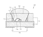
- FIG. 1 is a plan view of a light-emitting device package 100 according to example embodiments.
- FIG. 2 is a cross-sectional view taken along line II-II′ of FIG. 1 .
- a molding member and a lens unit are not depicted.
- the light-emitting device package 100 may include a pre-mold 110 formed of an upper body 111 and a lower body 112 .
- a plurality of lead frames 120 that surround a portion of the lower body 112 and are separate from each other are formed between the upper body 111 and the lower body 112 .
- the lead frames 120 may be a pair of lead frames.
- the pair of lead frames may include a first lead frame 121 and a second lead frame 122 .
- a light-emitting device 130 that emits light may be mounted on the first lead frame 121 .
- the light-emitting device 130 may be connected to the second lead frame 122 through a wire 140 .
- the pre-mold 110 supports and protects the light-emitting device 130 , and may be formed of one of polyphthalamide (PPA), liquid crystal polymer, and ceramic.
- PPA polyphthalamide
- the pre-mold 110 may have various shapes.
- the upper body 111 may include a inclined (e.g., concavely) plane 113 , a diameter of which gradually decreases towards the lower body 112 .
- a reflection unit 115 that upwardly reflects light emitted from the light-emitting device 130 may further be formed on the inclined (e.g., concavely) plane 113 .
- the reflection unit 115 may be formed by coating a material having a relatively high reflectance, e.g., Ag or Al, to effectively reflect light emitted from the light-emitting device 130 .
- the pre-mold 110 includes the upper body 111 and the lower body 112
- the upper body 111 and the lower body 112 may be formed as one body.
- a plurality of vertical holes 114 passing through the upper body 111 may be formed in the inclined (e.g., concavely) plane 113 .
- a plurality of holes 116 may be formed in the reflection unit 115 to connect to the vertical holes 114 .
- the vertical holes 114 may be formed substantially vertical to an upper surface of the lower body 112 .
- the vertical holes 114 may be formed concentrically in the inclined (e.g., concavely) plane 113 with a predetermined or given distance between each of the vertical holes.
- the vertical holes 114 may have a diameter in a range from about 0.1 mm to about 0.5 mm.
- the vertical holes 114 may expose upper surfaces of the lead frames 120 .
- the vertical holes 114 may be formed through a portion of the lower body 112 where the vertical holes 114 do not meet the lead frames 120 .
- the inclined (e.g., concavely) plane 113 of the upper body 111 and an upper surface 112 a of the lower body 112 form a concave unit.
- the concave unit may be filled with a molding member 150 to cover and protect the light-emitting device 130 and the wire 140 .
- the molding member 150 may also be filled in the vertical holes 114 .
- the molding member 150 may be formed of a transparent material, e.g., an epoxy resin or a silicon resin, so that light emitted from the light-emitting device 130 may be transmitted to the outside. Also, the molding member 150 may further include a diffuser that allows light emitted from the light-emitting device 130 to be uniformly emitted by scattering the light. The diffuser may be barium titanate, titanium oxide, or aluminum oxide. A phosphor may further be included in the molding member 150 . The phosphor may emit light having a wavelength different from that of light emitted from the light-emitting device 130 by absorbing a portion of the light.
- a transparent material e.g., an epoxy resin or a silicon resin
- the lead frames 120 supply an external power to the light-emitting device 130 .
- a portion of each of the first lead frame 121 and the second lead frame 122 may be interposed between the upper body 111 and the lower body 112 , and the other portion thereof may surround the lower body 112 .
- the light-emitting device 130 may have a compound semiconductor stacked structure having a PN junction structure, and may emit light by the recombination of electrons and holes supplied by applying power through the lead frames 120 .
- the light-emitting device 130 may be attached onto the upper surface of the first lead frame 121 to be electrically connected to the first lead frame 121 .
- the light-emitting device 130 may be attached to the first lead frame 121 through a conductive bond.
- a p-type electrode and an n-type electrode may be disposed on an upper surface and a lower surface of the light-emitting device 130 , respectively, and the n-type electrode may be attached to the first lead frame 121 and the p-type electrode may be connected to the second lead frame 122 through the wire 140 .
- the light-emitting device 130 of FIG. 2 is a vertical-type light-emitting device, example embodiments are not limited thereto.
- the light-emitting device 130 may be a horizontal-type light-emitting device which may be connected to the first lead frame 121 and the second lead frame 122 via wires, respectively.
- the wire 140 may connect the light-emitting device 130 to the first lead frame 121 , and may be formed of Au or Al.
- vertical holes may be formed in a inclined (e.g., concavely) plane of a pre-mold, and the vertical holes may be filled with a molding resin. Accordingly, a bonding force between the molding resin and the pre-mold is strong, and molding resin represses the contraction or expansion of the molding member in the vertical holes. Accordingly, even if a relatively severe vibration is applied to the light-emitting device package, the separation of the molding resin from the pre-mold is prevented or reduced, and thus, the disconnection of a wire that connects the light-emitting device to leads may be prevented or reduced.
Landscapes
- Led Device Packages (AREA)
Abstract
Description
Claims (18)
Applications Claiming Priority (2)
| Application Number | Priority Date | Filing Date | Title |
|---|---|---|---|
| KR1020120051650A KR20130127838A (en) | 2012-05-15 | 2012-05-15 | The light- |
| KR10-2012-0051650 | 2012-05-15 |
Publications (2)
| Publication Number | Publication Date |
|---|---|
| US20130307003A1 US20130307003A1 (en) | 2013-11-21 |
| US8860073B2 true US8860073B2 (en) | 2014-10-14 |
Family
ID=49580598
Family Applications (1)
| Application Number | Title | Priority Date | Filing Date |
|---|---|---|---|
| US13/709,302 Active 2033-04-10 US8860073B2 (en) | 2012-05-15 | 2012-12-10 | Light-emitting device package |
Country Status (2)
| Country | Link |
|---|---|
| US (1) | US8860073B2 (en) |
| KR (1) | KR20130127838A (en) |
Families Citing this family (8)
| Publication number | Priority date | Publication date | Assignee | Title |
|---|---|---|---|---|
| US20160079217A1 (en) * | 2014-09-12 | 2016-03-17 | Kabushiki Kaisha Toshiba | Semiconductor light emitting device and lead frame |
| KR20160069161A (en) * | 2014-12-08 | 2016-06-16 | 엘지이노텍 주식회사 | Light emitting module |
| KR102432859B1 (en) * | 2015-07-10 | 2022-08-16 | 삼성전자주식회사 | Light emitting device and Light emitting module including the same |
| KR102506588B1 (en) * | 2017-09-19 | 2023-03-07 | 서울바이오시스 주식회사 | Light emitting diode package |
| US10615319B2 (en) * | 2017-10-20 | 2020-04-07 | Nichia Corporation | Light emitting device |
| KR102133296B1 (en) | 2019-11-22 | 2020-07-13 | 박찬정 | Manual Lifter For Loading Weight On Vehicle's Cargo |
| JP7370274B2 (en) * | 2020-02-18 | 2023-10-27 | 日機装株式会社 | Semiconductor packages and semiconductor light emitting devices |
| US20250287740A1 (en) * | 2024-03-06 | 2025-09-11 | Creeled, Inc. | Anchored encapsulation in led devices |
Citations (10)
| Publication number | Priority date | Publication date | Assignee | Title |
|---|---|---|---|---|
| US20030168720A1 (en) * | 2002-03-06 | 2003-09-11 | Nichia Corporation | Semiconductor device and manufacturing method for same |
| JP2003282955A (en) | 2001-07-19 | 2003-10-03 | Rohm Co Ltd | Semiconductor light-emitting device having reflector case |
| US20060022215A1 (en) * | 2003-01-30 | 2006-02-02 | Karlheinz Arndt | Semiconductor component emitting and/or receiving electromagnetic radiation, and housing base for such a component |
| US20060102918A1 (en) * | 2004-11-16 | 2006-05-18 | Wen-Lung Su | Package Structure of a Surface Mount Device Light Emitting Diode |
| KR100665262B1 (en) | 2005-10-20 | 2007-01-09 | 삼성전기주식회사 | LED Package |
| JP2007305785A (en) | 2006-05-11 | 2007-11-22 | Nichia Chem Ind Ltd | Light emitting device |
| JP2009099923A (en) | 2007-09-29 | 2009-05-07 | Kyocera Corp | Light emitting element storage package, light emitting device, light emitting element storage package, and light emitting device manufacturing method |
| US20090134408A1 (en) * | 2007-11-28 | 2009-05-28 | Samsung Electronics Co., Ltd. | Light emitting diode package, method of fabricating the same and backlight assembly including the same |
| US20100072506A1 (en) * | 2006-09-28 | 2010-03-25 | Seoul Opto Device Co., Ltd. | Ultraviolet light emitting diode package |
| JP2010129655A (en) | 2008-11-26 | 2010-06-10 | Toyoda Gosei Co Ltd | Led light emitting device |
-
2012
- 2012-05-15 KR KR1020120051650A patent/KR20130127838A/en not_active Ceased
- 2012-12-10 US US13/709,302 patent/US8860073B2/en active Active
Patent Citations (10)
| Publication number | Priority date | Publication date | Assignee | Title |
|---|---|---|---|---|
| JP2003282955A (en) | 2001-07-19 | 2003-10-03 | Rohm Co Ltd | Semiconductor light-emitting device having reflector case |
| US20030168720A1 (en) * | 2002-03-06 | 2003-09-11 | Nichia Corporation | Semiconductor device and manufacturing method for same |
| US20060022215A1 (en) * | 2003-01-30 | 2006-02-02 | Karlheinz Arndt | Semiconductor component emitting and/or receiving electromagnetic radiation, and housing base for such a component |
| US20060102918A1 (en) * | 2004-11-16 | 2006-05-18 | Wen-Lung Su | Package Structure of a Surface Mount Device Light Emitting Diode |
| KR100665262B1 (en) | 2005-10-20 | 2007-01-09 | 삼성전기주식회사 | LED Package |
| JP2007305785A (en) | 2006-05-11 | 2007-11-22 | Nichia Chem Ind Ltd | Light emitting device |
| US20100072506A1 (en) * | 2006-09-28 | 2010-03-25 | Seoul Opto Device Co., Ltd. | Ultraviolet light emitting diode package |
| JP2009099923A (en) | 2007-09-29 | 2009-05-07 | Kyocera Corp | Light emitting element storage package, light emitting device, light emitting element storage package, and light emitting device manufacturing method |
| US20090134408A1 (en) * | 2007-11-28 | 2009-05-28 | Samsung Electronics Co., Ltd. | Light emitting diode package, method of fabricating the same and backlight assembly including the same |
| JP2010129655A (en) | 2008-11-26 | 2010-06-10 | Toyoda Gosei Co Ltd | Led light emitting device |
Also Published As
| Publication number | Publication date |
|---|---|
| US20130307003A1 (en) | 2013-11-21 |
| KR20130127838A (en) | 2013-11-25 |
Similar Documents
| Publication | Publication Date | Title |
|---|---|---|
| US8860073B2 (en) | Light-emitting device package | |
| US11515296B2 (en) | Light-emitting device, integrated light-emitting device, and light-emitting module | |
| CN103026512B (en) | Device and the method for the manufacture of device | |
| TWI712181B (en) | Light-emitting device, integrated light-emitting device, and light-emitting module | |
| US11929456B2 (en) | Solid-state radiation transducer devices having flip-chip mounted solid-state radiation transducers and associated systems and methods | |
| US9130137B2 (en) | Light emitting element and light emitting module thereof | |
| CN109952660B (en) | Light emitting diode package | |
| US20120268916A1 (en) | Light emitting device package and method of manufacturing the same | |
| KR20090004078A (en) | Light emitting device package | |
| US8847270B2 (en) | LED package with recess and protrusions | |
| US11081630B2 (en) | Light emitting device package with a coating layer | |
| KR20120040549A (en) | Led light source module and method of manufacturing the same | |
| KR102025719B1 (en) | Light emitting device package and method of manufacturing the same | |
| KR20120075452A (en) | Light emitting diode having improved luminous efficiency |
Legal Events
| Date | Code | Title | Description |
|---|---|---|---|
| AS | Assignment |
Owner name: SAMSUNG ELECTRONICS CO., LTD., KOREA, REPUBLIC OF Free format text: ASSIGNMENT OF ASSIGNORS INTEREST;ASSIGNORS:PARK, HUN-YONG;KIM, CHOO-HO;JUNG, WON-HO;AND OTHERS;REEL/FRAME:029474/0491 Effective date: 20121205 |
|
| STCF | Information on status: patent grant |
Free format text: PATENTED CASE |
|
| MAFP | Maintenance fee payment |
Free format text: PAYMENT OF MAINTENANCE FEE, 4TH YEAR, LARGE ENTITY (ORIGINAL EVENT CODE: M1551) Year of fee payment: 4 |
|
| MAFP | Maintenance fee payment |
Free format text: PAYMENT OF MAINTENANCE FEE, 8TH YEAR, LARGE ENTITY (ORIGINAL EVENT CODE: M1552); ENTITY STATUS OF PATENT OWNER: LARGE ENTITY Year of fee payment: 8 |
|
| MAFP | Maintenance fee payment |
Free format text: PAYMENT OF MAINTENANCE FEE, 12TH YEAR, LARGE ENTITY (ORIGINAL EVENT CODE: M1553); ENTITY STATUS OF PATENT OWNER: LARGE ENTITY Year of fee payment: 12 |