US8841179B2 - Nitride semiconductor device using selective growth and manufacturing method thereof - Google Patents
Nitride semiconductor device using selective growth and manufacturing method thereof Download PDFInfo
- Publication number
- US8841179B2 US8841179B2 US13/673,436 US201213673436A US8841179B2 US 8841179 B2 US8841179 B2 US 8841179B2 US 201213673436 A US201213673436 A US 201213673436A US 8841179 B2 US8841179 B2 US 8841179B2
- Authority
- US
- United States
- Prior art keywords
- gan layer
- layer
- type gan
- semiconductor device
- gate electrode
- Prior art date
- Legal status (The legal status is an assumption and is not a legal conclusion. Google has not performed a legal analysis and makes no representation as to the accuracy of the status listed.)
- Active
Links
Images


Classifications
-
- H—ELECTRICITY
- H10—SEMICONDUCTOR DEVICES; ELECTRIC SOLID-STATE DEVICES NOT OTHERWISE PROVIDED FOR
- H10D—INORGANIC ELECTRIC SEMICONDUCTOR DEVICES
- H10D30/00—Field-effect transistors [FET]
- H10D30/80—FETs having rectifying junction gate electrodes
- H10D30/87—FETs having Schottky gate electrodes, e.g. metal-semiconductor FETs [MESFET]
-
- H01L29/7783—
-
- H—ELECTRICITY
- H10—SEMICONDUCTOR DEVICES; ELECTRIC SOLID-STATE DEVICES NOT OTHERWISE PROVIDED FOR
- H10D—INORGANIC ELECTRIC SEMICONDUCTOR DEVICES
- H10D62/00—Semiconductor bodies, or regions thereof, of devices having potential barriers
- H10D62/10—Shapes, relative sizes or dispositions of the regions of the semiconductor bodies; Shapes of the semiconductor bodies
- H10D62/102—Constructional design considerations for preventing surface leakage or controlling electric field concentration
- H10D62/103—Constructional design considerations for preventing surface leakage or controlling electric field concentration for increasing or controlling the breakdown voltage of reverse-biased devices
- H10D62/105—Constructional design considerations for preventing surface leakage or controlling electric field concentration for increasing or controlling the breakdown voltage of reverse-biased devices by having particular doping profiles, shapes or arrangements of PN junctions; by having supplementary regions, e.g. junction termination extension [JTE]
- H10D62/106—Constructional design considerations for preventing surface leakage or controlling electric field concentration for increasing or controlling the breakdown voltage of reverse-biased devices by having particular doping profiles, shapes or arrangements of PN junctions; by having supplementary regions, e.g. junction termination extension [JTE] having supplementary regions doped oppositely to or in rectifying contact with regions of the semiconductor bodies, e.g. guard rings with PN or Schottky junctions
-
- H01L21/2056—
-
- H01L29/1054—
-
- H01L29/66522—
-
- H—ELECTRICITY
- H10—SEMICONDUCTOR DEVICES; ELECTRIC SOLID-STATE DEVICES NOT OTHERWISE PROVIDED FOR
- H10D—INORGANIC ELECTRIC SEMICONDUCTOR DEVICES
- H10D30/00—Field-effect transistors [FET]
- H10D30/01—Manufacture or treatment
- H10D30/015—Manufacture or treatment of FETs having heterojunction interface channels or heterojunction gate electrodes, e.g. HEMT
-
- H—ELECTRICITY
- H10—SEMICONDUCTOR DEVICES; ELECTRIC SOLID-STATE DEVICES NOT OTHERWISE PROVIDED FOR
- H10D—INORGANIC ELECTRIC SEMICONDUCTOR DEVICES
- H10D30/00—Field-effect transistors [FET]
- H10D30/01—Manufacture or treatment
- H10D30/021—Manufacture or treatment of FETs having insulated gates [IGFET]
-
- H—ELECTRICITY
- H10—SEMICONDUCTOR DEVICES; ELECTRIC SOLID-STATE DEVICES NOT OTHERWISE PROVIDED FOR
- H10D—INORGANIC ELECTRIC SEMICONDUCTOR DEVICES
- H10D30/00—Field-effect transistors [FET]
- H10D30/40—FETs having zero-dimensional [0D], one-dimensional [1D] or two-dimensional [2D] charge carrier gas channels
- H10D30/47—FETs having zero-dimensional [0D], one-dimensional [1D] or two-dimensional [2D] charge carrier gas channels having two-dimensional [2D] charge carrier gas channels, e.g. nanoribbon FETs or high electron mobility transistors [HEMT]
- H10D30/471—High electron mobility transistors [HEMT] or high hole mobility transistors [HHMT]
- H10D30/473—High electron mobility transistors [HEMT] or high hole mobility transistors [HHMT] having confinement of carriers by multiple heterojunctions, e.g. quantum well HEMT
- H10D30/4732—High electron mobility transistors [HEMT] or high hole mobility transistors [HHMT] having confinement of carriers by multiple heterojunctions, e.g. quantum well HEMT using Group III-V semiconductor material
-
- H—ELECTRICITY
- H10—SEMICONDUCTOR DEVICES; ELECTRIC SOLID-STATE DEVICES NOT OTHERWISE PROVIDED FOR
- H10D—INORGANIC ELECTRIC SEMICONDUCTOR DEVICES
- H10D30/00—Field-effect transistors [FET]
- H10D30/40—FETs having zero-dimensional [0D], one-dimensional [1D] or two-dimensional [2D] charge carrier gas channels
- H10D30/47—FETs having zero-dimensional [0D], one-dimensional [1D] or two-dimensional [2D] charge carrier gas channels having two-dimensional [2D] charge carrier gas channels, e.g. nanoribbon FETs or high electron mobility transistors [HEMT]
- H10D30/471—High electron mobility transistors [HEMT] or high hole mobility transistors [HHMT]
- H10D30/475—High electron mobility transistors [HEMT] or high hole mobility transistors [HHMT] having wider bandgap layer formed on top of lower bandgap active layer, e.g. undoped barrier HEMTs such as i-AlGaN/GaN HEMTs
-
- H—ELECTRICITY
- H10—SEMICONDUCTOR DEVICES; ELECTRIC SOLID-STATE DEVICES NOT OTHERWISE PROVIDED FOR
- H10D—INORGANIC ELECTRIC SEMICONDUCTOR DEVICES
- H10D30/00—Field-effect transistors [FET]
- H10D30/60—Insulated-gate field-effect transistors [IGFET]
- H10D30/751—Insulated-gate field-effect transistors [IGFET] having composition variations in the channel regions
-
- H01L29/2003—
-
- H—ELECTRICITY
- H10—SEMICONDUCTOR DEVICES; ELECTRIC SOLID-STATE DEVICES NOT OTHERWISE PROVIDED FOR
- H10D—INORGANIC ELECTRIC SEMICONDUCTOR DEVICES
- H10D62/00—Semiconductor bodies, or regions thereof, of devices having potential barriers
- H10D62/80—Semiconductor bodies, or regions thereof, of devices having potential barriers characterised by the materials
- H10D62/85—Semiconductor bodies, or regions thereof, of devices having potential barriers characterised by the materials being Group III-V materials, e.g. GaAs
- H10D62/8503—Nitride Group III-V materials, e.g. AlN or GaN
-
- H—ELECTRICITY
- H10—SEMICONDUCTOR DEVICES; ELECTRIC SOLID-STATE DEVICES NOT OTHERWISE PROVIDED FOR
- H10D—INORGANIC ELECTRIC SEMICONDUCTOR DEVICES
- H10D64/00—Electrodes of devices having potential barriers
- H10D64/60—Electrodes characterised by their materials
- H10D64/602—Heterojunction gate electrodes for FETs
-
- H—ELECTRICITY
- H10—SEMICONDUCTOR DEVICES; ELECTRIC SOLID-STATE DEVICES NOT OTHERWISE PROVIDED FOR
- H10P—GENERIC PROCESSES OR APPARATUS FOR THE MANUFACTURE OR TREATMENT OF DEVICES COVERED BY CLASS H10
- H10P14/00—Formation of materials, e.g. in the shape of layers or pillars
- H10P14/20—Formation of materials, e.g. in the shape of layers or pillars of semiconductor materials
- H10P14/24—Formation of materials, e.g. in the shape of layers or pillars of semiconductor materials using chemical vapour deposition [CVD]
-
- H—ELECTRICITY
- H10—SEMICONDUCTOR DEVICES; ELECTRIC SOLID-STATE DEVICES NOT OTHERWISE PROVIDED FOR
- H10P—GENERIC PROCESSES OR APPARATUS FOR THE MANUFACTURE OR TREATMENT OF DEVICES COVERED BY CLASS H10
- H10P14/00—Formation of materials, e.g. in the shape of layers or pillars
- H10P14/20—Formation of materials, e.g. in the shape of layers or pillars of semiconductor materials
- H10P14/34—Deposited materials, e.g. layers
- H10P14/3402—Deposited materials, e.g. layers characterised by the chemical composition
- H10P14/3414—Deposited materials, e.g. layers characterised by the chemical composition being group IIIA-VIA materials
- H10P14/3416—Nitrides
Definitions
- the present invention relates to a nitride semiconductor device using selective growth and a manufacturing method thereof.
- a nitride semiconductor having the characteristics of a high threshold electric field, low ON resistance, resistance to high temperature, and high frequency operational characteristics, in comparison to silicon, has been studied as a material of a next-generation semiconductor device.
- High output power devices include a metal-oxide-semiconductor field-effect transistor (MOSFET) and an insulated gate bipolar mode transistor (IGBT) as the mainstream, and recently, GaN-based devices such as high electron mobility transistor (HEMT), hetero-junction field effect transistor (HFET), MOSFET, and the like, have been studied.
- MOSFET metal-oxide-semiconductor field-effect transistor
- IGBT insulated gate bipolar mode transistor
- GaN-based devices such as high electron mobility transistor (HEMT), hetero-junction field effect transistor (HFET), MOSFET, and the like, have been studied.
- the HEMT In the case of the HEMT, it is used in a communication device having HF characteristics, or the like, by using high electron mobility, but in the case of the MOSFET, its effect is not remarkable due to an absence of a gate oxide film having excellent characteristics, difficulty in ion implantation and thermal diffusion for selectively forming a P type or N type region, or the like, over the physical characteristics of GaN.
- FIG. 1 is an exemplary view showing a general structure of a hetero-junction field effect transistor (HFET).
- HFET hetero-junction field effect transistor
- a switching operation may be performed on a 2DEG (two-dimensional electron gas) current flowing from a drain electrode to a source electrode, through a schottky gate electrode.
- 2DEG two-dimensional electron gas
- a general HFET 10 may include a substrate (not shown), a first GaN layer 11 , an AlGaN layer 12 formed on the first GaN layer, a second GaN layer 13 formed on the AlGaN layer, a gate electrode 14 formed on the second GaN layer, a source electrode 15 , and a drain electrode 16 .
- An aspect of the present invention provides a semiconductor device including a first GaN layer, an AlGaN layer, a second GaN layer, a gate electrode, a source electrode, and a drain electrode sequentially stacked on a substrate, wherein a p type GaN layer is formed on the AlGaN layer to thereby reduce or remove a leakage current generated in a gate electrode and improve breakdown voltage characteristics, and a manufacturing method thereof.
- the p type GaN layer in forming the p type GaN layer, can be re-grown horizontally, rather than, vertically, on the exposed (or open) second GaN layer by using a local oxidation film mask pattern.
- a semiconductor device having high reliability by minimizing lattice defect or a dislocation density and enhancing crystalline is provided.
- a semiconductor device including: a substrate; a first GaN layer formed on the substrate; an AlGaN layer formed on the first GaN layer; a second GaN layer formed on the AlGaN layer and including a p type GaN layer; and a gate electrode formed on the second GaN layer, wherein the p type GaN layer may be in contact with a portion of the gate electrode.
- the second GaN layer may have a recess, and the p type GaN layer may be formed on the recess.
- the p type GaN layer may include a first layer and a second layer, and the first layer may be in contact with a lower portion of one side of the gate electrode, and the second layer may be in contact with a lower portion of the other side of the gate electrode.
- the p type GaN layer may include a plurality of layers, and the plurality of layers may be disposed to be spaced from one another in a horizontal direction.
- the p type GaN layer may be in contact with a portion of the AlGaN layer.
- the second GaN layer may have a hole, and the p type GaN layer may be formed to be insertedly formed in the hole.
- the p type GaN layer may be formed based on at least one of metal-organic chemical vapor deposition (MOCVD), molecular beam epitaxy (MBE), and hydride vapor phase epitaxy (HVPE).
- MOCVD metal-organic chemical vapor deposition
- MBE molecular beam epitaxy
- HVPE hydride vapor phase epitaxy
- the p type GaN layer may be formed to have a thickness ranging from 1 nm to 100 nm.
- the p type GaN layer may have at least one of a trench shape, a V-groove shape, and a hemispherical shape.
- a concentration of p type impurities of the p type GaN layer may be within the range of 1e 17 /cm 3 ⁇ 1e 21 /cm 3 .
- the concentration of p type impurities of the p type GaN layer may be successively changed in a particular direction and by a particular slope.
- the p type GaN layer may be magnesium (Mg).
- a method for manufacturing a semiconductor device including: forming a first GaN layer on a substrate; forming an AlGaN layer on the first GaN layer; forming a second GaN layer on the AlGaN layer; forming an oxide film layer on the second GaN layer; selectively etching the oxide film layer to define a p type GaN region; etching the p type GaN region to form a recess on the second GaN layer; forming a p type GaN layer on the recess; removing the oxide film layer; and forming a gate electrode on the second GaN layer, wherein the p type GaN layer may be formed to be in contact with a portion of the gate electrode.
- the oxide film layer may include SiO 2 .
- the oxide film layer may be formed to have a thickness ranging from 50 nm to 1000 nm.
- a semiconductor device including a first GaN layer, an AlGaN layer, a second GaN layer, a gate electrode, a source electrode, and a drain electrode sequentially stacked on a substrate, wherein a p type GaN layer is formed on the AlGaN layer to thereby reduce or remove a leakage current generated in a gate electrode and improve breakdown voltage characteristics, and a manufacturing method thereof, are provided.
- the p type GaN layer is locally formed on the AlGaN layer, a leakage of the gate electrode can be minimized and a depletion region is enlarged to allow a threshold voltage (supply voltage) to move in a positive direction.
- a lattice defect or dislocation density is minimized and crystalline is enhanced, thus increasing reliability of the device.
- FIG. 1 is an exemplary view illustrating a general structure of a hetero-junction field effect transistor (HFET).
- HFET hetero-junction field effect transistor
- FIG. 2 is an exemplary view illustrating a structure of a semiconductor device according to embodiments disclosed in the present disclosure.
- FIGS. 3A and 3D are exemplary views illustrating various dispositions of a p type GaN layer according to a first embodiment disclosed in the present disclosure.
- FIGS. 4A and 4C are exemplary views illustrating various dispositions of a p type GaN layer according to a second embodiment disclosed in the present disclosure.
- FIGS. 5A to 5I are exemplary views illustrating a method for manufacturing a semiconductor device according to embodiments disclosed in the present disclosure.
- a technique disclosed in the present disclosure may be applied to a hetero-junction field effect transistor (HFET) and a manufacturing method thereof.
- the technique disclosed in the present disclosure is not limited thereto and may be applicable to any nitride-based semiconductor device and a manufacturing method thereof to which the technical concept of the technique is applicable.
- the technique may be applied to locally forming a p type GaN layer below a gate electrode of a nitride semiconductor device to move a threshold voltage (supply voltage) of the semiconductor device in a positive direction.
- first and second may be used to describe various components, such components must not be understood as being limited to the above terms. The above terms are used only to distinguish one component from another. For example, a first component may be referred to as a second component without departing from the scope of rights of the present invention, and likewise a second component may be referred to as a first component.
- a semiconductor device may include a substrate, a first GaN layer formed on the substrate, an AlGaN layer formed on the first GaN layer, a second GaN layer formed on the AlGaN layer and including a p type GaN layer, and a gate electrode formed on the second GaN layer, wherein the p type GaN layer may be in contact with a portion of the gate electrode.
- the second GaN layer may have a recess, and the p type GaN layer may be formed on the recess.
- the p type GaN layer may include a first layer and a second layer, and the first layer may be in contact with a lower portion of one side of the gate electrode, and the second layer may be in contact with a lower portion of the other side of the gate electrode.
- the p type GaN layer may include a plurality of layers, and the plurality of layers may be disposed to be spaced from one another in a horizontal direction.
- the p type GaN layer may be in contact with a portion of the AlGaN layer.
- the second GaN layer may have a hole, and the p type GaN layer may be formed to be insertedly formed in the hole.
- the p type GaN layer may be formed based on at least one of metal-organic chemical vapor deposition (MOCVD), molecular beam epitaxy (MBE), and hydride vapor phase epitaxy (HVPE).
- MOCVD metal-organic chemical vapor deposition
- MBE molecular beam epitaxy
- HVPE hydride vapor phase epitaxy
- the p type GaN layer may be formed to have a thickness ranging from 1 nm to 100 nm.
- the p type GaN layer may have at least one of a trench shape, a V-groove shape, and a hemispherical shape.
- a concentration of p type impurities of the p type GaN layer may be within the range of 1e 17 /cm 3 ⁇ 1e 21 /cm 3 .
- the concentration of p type impurities of the p type GaN layer may be successively changed in a particular direction and by a particular slope.
- the p type GaN layer may be magnesium (Mg).
- FIG. 2 is an exemplary view illustrating a structure of a semiconductor device according to embodiments disclosed in the present disclosure.
- a semiconductor device 100 may include a p type GaN layer forming a depletion layer according to a gate voltage applied to a gate electrode.
- the semiconductor device 100 may include a substrate (not shown), a first GaN layer 110 formed on the substrate, an AlGaN layer 120 formed on the first GaN layer, a second GaN layer formed on the AlGaN layer and having recesses, a gate electrode 140 formed on the second GaN layer 130 , and a p type GaN layer 170 formed on the recesses, wherein the p type GaN layer may be in contact with a portion of the gate electrode 140 .
- the substrate can be removed after fabrication of the semiconductor device 100 . Therefore, the semiconductor device 100 may have a final structure without the substrate.
- the semiconductor device 100 may include a source electrode 150 and a drain electrode 160 , and a DEG current flowing from the drain electrode 160 to the source electrode 150 may be switched through the schottky gate electrode.
- the p type GaN layer 170 is formed above the AlGaN layer 120 , a leakage current and a breakdown voltage characteristics generated in the gate electrode 140 can be enhanced.
- the p type GaN layer 170 may serve to form a gate depletion region having high crystalline, a leakage current and breakdown voltage characteristics can be enhanced.
- the p type GaN layer 170 may be formed according to various methods.
- the p type GaN layer 170 may be formed by implanting ions for selectively forming a p type and activating it through annealing.
- the p type GaN layer 170 may be formed through a method for selectively growing a nitride semiconductor crystal.
- the p type GaN layer 170 may be formed based on at least one of metal-organic chemical vapor deposition (MOCVD), molecular beam epitaxy (MBE), and hydride vapor phase epitaxy (HVPE).
- MOCVD metal-organic chemical vapor deposition
- MBE molecular beam epitaxy
- HVPE hydride vapor phase epitaxy
- the MOCVD method is generally used.
- a method for selectively growing crystal may be advantageous in that it does not damage a semiconductor surface, not affecting GaN itself.
- the method for selectively growing crystal is advantageous in that a process is facilitated because the p type GaN layer 170 structure can be manufactured only through etching and re-growing.
- the p type GaN layer 170 is grown in a horizontal direction, rather than in a vertical direction in which dislocation, a defect, or the like, is formed therealong, whereby a lattice defect or a dislocation density can be significantly reduced.
- reliability considered to be the most important in a power device can be increased by reducing a defect density of crystal.
- various other methods for forming the p type GaN layer 170 may be applied to the method for manufacturing a semiconductor device disclosed in the present disclosure.
- the p type GaN layer 170 may be formed to have various thicknesses.
- the p type GaN layer 170 may be formed to have a thickness ranging from 1 nm to 100 nm.
- the p type GaN layer 170 may be formed to have a thickness ranging from 5 nm to 10 nm.
- the p type GaN layer 170 is formed to have various other thicknesses.
- the p type GaN layer 170 may include various p type impurities.
- the p type impurities of the p type GaN layer 170 may be magnesium (Mg).
- Mg magnesium
- the p type GaN layer 170 includes various other p type impurities.
- the p type impurities of the p type GaN layer 170 may have various concentrations.
- the concentration of the p type impurities of the p type GaN layer 170 may be within a range of 1e 17 /cm 3 ⁇ 1e 21 /cm 3 .
- the concentration of the p type impurities of the p type GaN layer 170 may be within a range of 1e 18 /cm 3 ⁇ 1e 20 /cm 3 .
- the p type impurities of the p type GaN layer 170 may have various concentration distributions.
- the p type impurities of the p type GaN layer 170 may have a uniform concentration distribution within the p type GaN layer 170 .
- the p type impurities of the p type GaN layer 170 may have a concentration distribution successively changing in a particular direction and by a particular slope.
- a first embodiment disclosed in the present disclosure may be implemented by a portion or combination of the components or steps included in the foregoing embodiments or may be implemented by a combination of the embodiments.
- repeated portions may be omitted for clarity of the first embodiment of the present disclosure.
- a semiconductor device may include a substrate, a first GaN layer formed on the substrate, an AlGaN layer formed on the first GaN layer, a second GaN layer formed on the AlGaN layer and including a p type GaN layer, and a gate electrode formed on the second GaN layer, wherein the p type GaN layer may be in contact with a portion of the gate electrode.
- the second GaN layer may have a recess, and the p type GaN layer may be formed on the recess.
- the p type GaN layer may include a first layer and a second layer, and the first layer may be in contact with a lower portion of one side of the gate electrode, and the second layer may be in contact with a lower portion of the other side of the gate electrode.
- the p type GaN layer may include a plurality of layers, and the plurality of layers may be disposed to be spaced from one another in a horizontal direction.
- the p type GaN layer may be in contact with a portion of the AlGaN layer.
- the second GaN layer may have a hole, and the p type GaN layer may be formed to be insertedly formed in the hole.
- FIGS. 3A and 3D are exemplary views illustrating various dispositions of the p type GaN layer according to the first embodiment disclosed in the present disclosure.
- the p type GaN layer according to the first embodiment of the present invention may be formed according to various disposition schemes.
- the p type GaN layer 170 may be configured as a single layer 170 a and formed to be in contact with a portion of a lower surface of the gate electrode 140 as shown in FIG. 3A .
- the p type GaN layer 170 may include a first layer 170 b and a second layer 170 c , and the first layer 170 b may be in contact with a lower portion of one side of the gate electrode 140 , and the second layer 170 c may be in contact with a lower portion of the other side of the gate electrode 140 as shown in FIG. 3B .
- the p type GaN layer 170 may include a plurality of layers 170 d , and the plurality of layers 170 d may be formed to be disposed to be spaced apart from one another in a horizontal direction as shown in FIG. 3C .
- the p type GaN layer 170 may be in contact with a portion of the AlGaN layer 120 .
- the p type GaN layer 170 may be in contact with a portion of the AlGaN layer 120 in various manners.
- the second GaN layer 130 may have a hole, and the p type GaN layer 170 may be insertedly formed in the hole as shown in FIG. 3D .
- a second embodiment disclosed in the present disclosure may be implemented by a portion or combination of the components or steps included in the foregoing embodiments or may be implemented by a combination of the embodiments.
- repeated portions may be omitted for clarity of the second embodiment of the present disclosure.
- a semiconductor device may include a substrate, a first GaN layer formed on the substrate, an AlGaN layer formed on the first GaN layer, a second GaN layer formed on the AlGaN layer and including a p type GaN layer, and a gate electrode formed on the second GaN layer, wherein the p type GaN layer may be in contact with a portion of the gate electrode.
- the second GaN layer may have a recess, and the p type GaN layer may be formed on the recess.
- the p type GaN layer may be formed to have at least one of a trench shape, a V-groove shape, and a hemispherical shape.
- FIGS. 4A and 4C are exemplary views illustrating various dispositions of a p type GaN layer according to a second embodiment disclosed in the present disclosure.
- the p type GaN layer 170 may have various shapes.
- the p type GaN layer 170 may be a p type GaN layer 170 e having a trench shape as shown in FIG. 4A .
- the p type GaN layer 170 may be a p type GaN layer 170 f having a V-groove shape as shown in FIG. 4B .
- the p type GaN layer 170 may be a p type GaN layer 170 g having a hemispherical shape as shown in FIG. 4C .
- a method for manufacturing a semiconductor device may include forming a first GaN layer on a substrate; forming an AlGaN layer on the first GaN layer; forming a second GaN layer on the AlGaN layer; forming an oxide film layer on the second GaN layer; selectively etching the oxide film layer to define a p type GaN region; etching the p type GaN region to form a recess on the second GaN layer; forming a p type GaN layer on the recess; removing the oxide film layer; and forming a gate electrode on the second GaN layer, wherein the p type GaN layer may be formed to be in contact with a portion of the gate electrode.
- the p type GaN layer may include a first layer and a second layer, and the first layer may be in contact with a portion at one side of the gate electrode, and the second layer may be in contact with a portion at the other side of the gate electrode.
- the p type GaN layer may be formed based on at least one of metal-organic chemical vapor deposition (MOCVD), molecular beam epitaxy (MBE), and hydride vapor phase epitaxy (HVPE).
- MOCVD metal-organic chemical vapor deposition
- MBE molecular beam epitaxy
- HVPE hydride vapor phase epitaxy
- the oxide film layer may include SiO 2 .
- the oxide film layer may be formed to have a thickness ranging from 50 nm to 1000 nm.
- the p type GaN layer may be formed to have a thickness ranging from 1 nm to 100 nm.
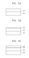
- FIGS. 5A to 5I are exemplary views illustrating a method for manufacturing a semiconductor device according to embodiments disclosed in the present disclosure.
- the method for manufacturing a semiconductor layer according to embodiments disclosed in the present disclosure may include the following steps.
- a first GaN layer 110 may be formed on a substrate 180 as shown in FIG. 5A , and an AlGaN layer 120 may be formed on the first GaN layer 110 as shown in FIG. 5B .
- the first GaN layer 110 may be grown on a silicon (Si) substrate or a sapphire substrate.
- the first GaN layer may be grown on a GaN substrate or an SiC substrate.
- the first GaN layer 110 may be formed through epitaxial growth by synthesizing TMGa as a material of gallium (Ga) and NH 3 as a material of nitrogen (N) in a reactor at a high temperature.
- the first GaN layer 110 may be formed through an organic metal vapor growth method called as an MOCVD method.
- the second GaN layer 130 may be formed on the AlGaN layer 120 as shown in FIG. 5C .
- the oxide film layer 190 may be formed on the second GaN layer 130 as shown in FIG. 5D .
- the oxide film layer 190 may boost growth of the p type GaN layer 170 in a horizontal direction, while restraining a growth thereof in a vertical direction.
- the oxide film layer 190 may be formed to have various thicknesses.
- the thickness of the oxide film layer 190 may range from 50 nm to 1000 nm.
- oxide film layers having various other thicknesses are applied to the method for manufacturing a semiconductor device according to an embodiment disclosed in the present disclosure.
- the oxide film layer 190 may be made of various materials.
- the oxide film layer 190 may be made of SiO 2 so as to be easily removed.
- the oxide film layer 190 is selectively etched to define p type GaN region 171 as shown in FIG. 5E .
- the p type GaN region 171 may be defined by forming a local pattern through a photoresist process and etching only a region desired to be deposited to thus expose a surface of the second GaN layer 130 .
- the p type GaN region 171 is etched to form a recess on the second GaN layer 130 . This may be to selectively grow the p type GaN layer 170 in a horizontal direction as shown in FIG. 5F .
- the p type GaN layer 170 may be formed in the recess as shown in FIG. 5G .
- the p type GaN layer 170 may be formed in a horizontal direction through a selective growth.
- p type impurities of the p type GaN layer 170 may be used as p type impurities of the p type GaN layer 170 .
- a dopant of the p type GaN layer 170 may be magnesium (Mg).
- the p type GaN layer 170 may be grown by doping magnesium (Mg) together with TMGa and NH 3 .
- the p type GaN layer 170 may include impurities having various concentrations.
- the concentration of p type impurities of the p type GaN layer 170 may be within the range of 1e 17 /cm 3 ⁇ 1e 21 /cm 3 .
- the concentration of p type impurities of the p type GaN layer 170 may be within the range of 1e 18 /cm 3 ⁇ 1e 20 /cm 3 .
- various p type impurity concentrations may be applied to form the p type GaN layer 170 .
- the p type GaN layer 170 may have various thicknesses.
- the p type GaN layer 170 may be formed to have a thickness ranging from 1 nm to 100 nm.
- the p type GaN layer 170 may be formed to have a thickness ranging from 5 nm to 10 nm.
- the p type GaN layer 170 may be formed to have various thicknesses.
- the oxide film layer 190 may be removed as shown in FIG. 5H .
- the oxide film layer 190 may be removed by using BOE etching chemical.
- the gate electrode 140 , the source electrode 150 , and the drain electrode 160 may be formed on the second GaN layer 130 as shown in FIG. 5I .
- an oxide film (not shown) may be formed on the second GaN layer 130 and the electrodes may be open.
Landscapes
- Junction Field-Effect Transistors (AREA)
- Electrodes Of Semiconductors (AREA)
- Chemical & Material Sciences (AREA)
- Engineering & Computer Science (AREA)
- Materials Engineering (AREA)
Abstract
Description
Claims (14)
Applications Claiming Priority (2)
| Application Number | Priority Date | Filing Date | Title |
|---|---|---|---|
| KR10-2011-0134771 | 2011-12-14 | ||
| KR1020110134771A KR101943356B1 (en) | 2011-12-14 | 2011-12-14 | Nitride semiconductor using selective growth and method thereof |
Publications (2)
| Publication Number | Publication Date |
|---|---|
| US20130153921A1 US20130153921A1 (en) | 2013-06-20 |
| US8841179B2 true US8841179B2 (en) | 2014-09-23 |
Family
ID=48609221
Family Applications (1)
| Application Number | Title | Priority Date | Filing Date |
|---|---|---|---|
| US13/673,436 Active US8841179B2 (en) | 2011-12-14 | 2012-11-09 | Nitride semiconductor device using selective growth and manufacturing method thereof |
Country Status (2)
| Country | Link |
|---|---|
| US (1) | US8841179B2 (en) |
| KR (1) | KR101943356B1 (en) |
Families Citing this family (5)
| Publication number | Priority date | Publication date | Assignee | Title |
|---|---|---|---|---|
| FR3010228B1 (en) * | 2013-08-30 | 2016-12-30 | St Microelectronics Tours Sas | PROCESS FOR TREATING A GALLIUM NITRIDE LAYER HAVING DISLOCATIONS |
| CN103579332B (en) * | 2013-10-31 | 2016-04-13 | 中航(重庆)微电子有限公司 | Hetero junction field effect pipe and preparation method thereof |
| KR102073790B1 (en) | 2013-12-09 | 2020-02-05 | 삼성전자주식회사 | Transmissive optical shutter and method of fabricating the same |
| CN106033724A (en) * | 2015-03-09 | 2016-10-19 | 中国科学院苏州纳米技术与纳米仿生研究所 | III-family nitride reinforced HEMT and preparation method thereof |
| CN105466970B (en) * | 2015-12-11 | 2018-02-13 | 北京大学 | For detecting the detection method and structure of trap states in gallium nitride radical heterojunction structure |
Citations (7)
| Publication number | Priority date | Publication date | Assignee | Title |
|---|---|---|---|---|
| US20070029573A1 (en) * | 2005-08-08 | 2007-02-08 | Lin Cheng | Vertical-channel junction field-effect transistors having buried gates and methods of making |
| US20080087915A1 (en) * | 2006-10-12 | 2008-04-17 | Yasuhiro Uemoto | Nitride semiconductor device and method for fabricating the same |
| US20100097105A1 (en) * | 2006-11-20 | 2010-04-22 | Tatsuo Morita | Semiconductor device and method for driving the same |
| US20100264460A1 (en) * | 2007-01-26 | 2010-10-21 | Grandusky James R | Thick pseudomorphic nitride epitaxial layers |
| US20100289122A1 (en) * | 2000-03-13 | 2010-11-18 | Cree, Inc. | Iii-v nitride substrate boule and method of making and using the same |
| US20110227093A1 (en) * | 2008-12-05 | 2011-09-22 | Panasonic Corporation | Field effect transistor and method of manufacturing the same |
| US8044409B2 (en) * | 2008-08-11 | 2011-10-25 | Taiwan Semiconductor Manufacturing Company, Ltd. | III-nitride based semiconductor structure with multiple conductive tunneling layer |
-
2011
- 2011-12-14 KR KR1020110134771A patent/KR101943356B1/en active Active
-
2012
- 2012-11-09 US US13/673,436 patent/US8841179B2/en active Active
Patent Citations (7)
| Publication number | Priority date | Publication date | Assignee | Title |
|---|---|---|---|---|
| US20100289122A1 (en) * | 2000-03-13 | 2010-11-18 | Cree, Inc. | Iii-v nitride substrate boule and method of making and using the same |
| US20070029573A1 (en) * | 2005-08-08 | 2007-02-08 | Lin Cheng | Vertical-channel junction field-effect transistors having buried gates and methods of making |
| US20080087915A1 (en) * | 2006-10-12 | 2008-04-17 | Yasuhiro Uemoto | Nitride semiconductor device and method for fabricating the same |
| US20100097105A1 (en) * | 2006-11-20 | 2010-04-22 | Tatsuo Morita | Semiconductor device and method for driving the same |
| US20100264460A1 (en) * | 2007-01-26 | 2010-10-21 | Grandusky James R | Thick pseudomorphic nitride epitaxial layers |
| US8044409B2 (en) * | 2008-08-11 | 2011-10-25 | Taiwan Semiconductor Manufacturing Company, Ltd. | III-nitride based semiconductor structure with multiple conductive tunneling layer |
| US20110227093A1 (en) * | 2008-12-05 | 2011-09-22 | Panasonic Corporation | Field effect transistor and method of manufacturing the same |
Also Published As
| Publication number | Publication date |
|---|---|
| KR20130067819A (en) | 2013-06-25 |
| US20130153921A1 (en) | 2013-06-20 |
| KR101943356B1 (en) | 2019-01-29 |
Similar Documents
| Publication | Publication Date | Title |
|---|---|---|
| US7084441B2 (en) | Semiconductor devices having a hybrid channel layer, current aperture transistors and methods of fabricating same | |
| US8575651B2 (en) | Devices having thick semi-insulating epitaxial gallium nitride layer | |
| CN101611473B (en) | Methods of fabricating semiconductor devices including implanted regions for providing low-resistance contact to buried layers and related devices | |
| US9184258B2 (en) | GaN based semiconductor device and method of manufacturing the same | |
| US9847401B2 (en) | Semiconductor device and method of forming the same | |
| US9443969B2 (en) | Transistor having metal diffusion barrier | |
| US20110042719A1 (en) | Semiconductor device and method of manufacturing a semiconductor device | |
| US20070164315A1 (en) | Cap Layers Including Aluminum Nitride for Nitride-Based Transistors and Methods of Fabricating Same | |
| US20110079822A1 (en) | Compound semiconductor device and manufacturing method | |
| CA2588114A1 (en) | Cap layers and/or passivation layers for nitride-based transistors, transistor structures and methods of fabricating same | |
| KR20140013247A (en) | Nitride based semiconductor device and preparing method for the same | |
| JP2007103451A (en) | Semiconductor device and manufacturing method thereof | |
| US8901609B1 (en) | Transistor having doped substrate and method of making the same | |
| US20240021719A1 (en) | Semiconductor device having doped seed layer and method of manufacturing the same | |
| US10134908B2 (en) | Semiconductor device and manufacturing method thereof | |
| JP2011187623A (en) | Semiconductor element and manufacturing method thereof | |
| US20130240900A1 (en) | Semiconductor device and method for producing the same | |
| KR102077674B1 (en) | Nitride semiconductor and method thereof | |
| US8841179B2 (en) | Nitride semiconductor device using selective growth and manufacturing method thereof | |
| KR20150091705A (en) | Nitride semiconductor and method thereof | |
| JP2006253224A (en) | Semiconductor device and manufacturing method thereof | |
| KR101951421B1 (en) | Nitride semiconductor device and method for manufacturing the same | |
| EP2117039A2 (en) | Semiconductor devices including shallow inplanted regions and methods of forming the same | |
| US20260101539A1 (en) | Group iii-n device with interspersed gate structure | |
| KR20150091704A (en) | Nitride semiconductor and method thereof |
Legal Events
| Date | Code | Title | Description |
|---|---|---|---|
| AS | Assignment |
Owner name: LG ELECTRONICS INC., KOREA, REPUBLIC OF Free format text: ASSIGNMENT OF ASSIGNORS INTEREST;ASSIGNORS:CHO, SEONGMOO;KIM, KWANGCHOONG;HWANG, EUJIN;AND OTHERS;SIGNING DATES FROM 20121024 TO 20121031;REEL/FRAME:029273/0090 |
|
| FEPP | Fee payment procedure |
Free format text: PAYOR NUMBER ASSIGNED (ORIGINAL EVENT CODE: ASPN); ENTITY STATUS OF PATENT OWNER: LARGE ENTITY |
|
| STCF | Information on status: patent grant |
Free format text: PATENTED CASE |
|
| MAFP | Maintenance fee payment |
Free format text: PAYMENT OF MAINTENANCE FEE, 4TH YEAR, LARGE ENTITY (ORIGINAL EVENT CODE: M1551) Year of fee payment: 4 |
|
| MAFP | Maintenance fee payment |
Free format text: PAYMENT OF MAINTENANCE FEE, 8TH YEAR, LARGE ENTITY (ORIGINAL EVENT CODE: M1552); ENTITY STATUS OF PATENT OWNER: LARGE ENTITY Year of fee payment: 8 |
|
| MAFP | Maintenance fee payment |
Free format text: PAYMENT OF MAINTENANCE FEE, 12TH YEAR, LARGE ENTITY (ORIGINAL EVENT CODE: M1553); ENTITY STATUS OF PATENT OWNER: LARGE ENTITY Year of fee payment: 12 |