US8830095B2 - Track and hold circuit and method - Google Patents
Track and hold circuit and method Download PDFInfo
- Publication number
- US8830095B2 US8830095B2 US13/770,003 US201313770003A US8830095B2 US 8830095 B2 US8830095 B2 US 8830095B2 US 201313770003 A US201313770003 A US 201313770003A US 8830095 B2 US8830095 B2 US 8830095B2
- Authority
- US
- United States
- Prior art keywords
- voltage
- circuit
- transistor
- gate
- hold
- Prior art date
- Legal status (The legal status is an assumption and is not a legal conclusion. Google has not performed a legal analysis and makes no representation as to the accuracy of the status listed.)
- Active
Links
Images


Classifications
-
- H—ELECTRICITY
- H03—ELECTRONIC CIRCUITRY
- H03M—CODING; DECODING; CODE CONVERSION IN GENERAL
- H03M1/00—Analogue/digital conversion; Digital/analogue conversion
- H03M1/12—Analogue/digital converters
- H03M1/124—Sampling or signal conditioning arrangements specially adapted for A/D converters
- H03M1/1245—Details of sampling arrangements or methods
-
- G—PHYSICS
- G11—INFORMATION STORAGE
- G11C—STATIC STORES
- G11C27/00—Electric analogue stores, e.g. for storing instantaneous values
- G11C27/02—Sample-and-hold arrangements
- G11C27/024—Sample-and-hold arrangements using a capacitive memory element
-
- G—PHYSICS
- G11—INFORMATION STORAGE
- G11C—STATIC STORES
- G11C27/00—Electric analogue stores, e.g. for storing instantaneous values
- G11C27/02—Sample-and-hold arrangements
- G11C27/024—Sample-and-hold arrangements using a capacitive memory element
- G11C27/026—Sample-and-hold arrangements using a capacitive memory element associated with an amplifier
Definitions
- This invention relates to track and hold circuits (also known as sample and hold circuits).
- a track and hold circuit needs to balance requirements for high speed, large bandwidth and linearity.
- these requirements are generally obtained by maintaining the gate-source voltage of the pass gate constant during the tracking phase relative to the input voltage.
- Vgs Gate-source voltage
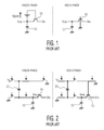
- FIG. 1 shows the typical known track and hold circuit.
- MOS transistor 10 in series between the input Vin and output Vout, with the source at the output and the drain at the input.
- the transistor functions as a pass gate, and will be referred to as the “main transistor”.
- the transistor In the tracking phase, the transistor is turned on, and a fixed gate-source voltage Vgson is applied to the transistor. This is shown in FIG. 1 as a voltage source between the output Vout and the transistor gate. In the track phase, the input and output voltages are equal (for a negligible drain-source voltage), so the voltage is copied from input to output.
- the output voltage is used to charge a capacitor 12 .
- the transistor In the hold phase, the transistor is turned off (shown in FIG. 1 by a grounded gate), and the capacitor 12 provides a constant output voltage for the duration of time before the next track phase.
- the pass gate In order to provide low charge injection, low input loading, and good isolation in the hold phase, the pass gate has to be efficient. There is also a minimum size of transistor for a given target value of the on resistance Ron.
- Vgson should be as high as possible (to switch the transistor hard on).
- the gate voltage (Vg) needs to exceed the supply voltage (Vdd) making the control difficult to implement.
- this is made possible by defining the gate voltage relative to the output (or input) voltage as shown in FIG. 1 , i.e. by fixing the gate-source voltage rather than the absolute gate voltage. This is a so-called “bootstrap” approach.
- FIG. 2 shows a track and hold circuit using a bootstrapped configuration in more detail.
- FIG. 2 uses a bootstrap capacitor 20 and a set of switches to implement the Vgson voltage step used in the circuit of FIG. 1 .
- the bootstrap capacitor 20 is connected in series between the source and gate. This means the bootstrap capacitor forces the gate voltage to be a fixed amount higher than the output voltage (which is equal to the input voltage).
- the gate of the main transistor 10 is connected to ground (in the same way as in FIG. 1 ), and the bootstrap capacitor is charged to the supply voltage, but is isolated from the output voltage.
- the bootstrap capacitor is recharged to the supply voltage, and this provides a voltage step by which the gate voltage exceeds the input/output voltage.
- the bootstrap circuit clearly occupies a significant area, with its storage capacitor and associated switches.
- a track and hold circuit comprising:
- main transistor between an input and an output of the circuit, wherein the main transistor is part of an integrated circuit supplied by a first set of voltage rails;
- a storage capacitor for storing the output voltage during a hold phase during which the main transistor is turned off
- a buffer circuit for generating a gate voltage for turning on the main transistor during a track phase, wherein the buffer circuit is adapted to derive a gate voltage based on the input or output voltage of the circuit and a voltage step, wherein the buffer circuit is supplied by a second set of voltage rails with a greater voltage swing than the first set of voltage rails.
- Each set of voltage rails typically comprises ground and at least one high voltage rail, for example in the range of 1V to 2V for the main transistor circuit and more than 2.5V for the buffer circuit.
- the main transistor circuit is typically part of a IC, for example a CMOS circuit.
- the buffer circuit can comprise a first, current source transistor, and a second transistor in series between voltage rails of the second set, wherein the node between the first and second transistors controls the gate voltage of the main transistor.
- the first transistor gate can be connected to a voltage derived from the high voltage rail of the second set and the second transistor gate is connected to the input or output.
- the current source transistor generates a current corresponding to the gate-source voltage applied, and this is mirrored to the gate-source of the second transistor. In this way, a voltage step is copied from the current source transistor onto the gate of the main transistor. This step can be larger than the maximum voltage of the first set of voltage rails.
- the node between the first and second transistors can be connected to gate of the main transistor.
- a hold transistor between the gate of the main transistor and ground can be used for implementing the hold phase, by shorting the main transistor gate to ground.
- the node between the first and second transistors is connected to a control transistor gate, and the control transistor is connected between a voltage rail of the second set of voltage rails and the gate of the main transistor.
- a hold transistor can again be provided between the gate of the main transistor and ground for implementing the hold phase.
- a current source can be provided for driving a current through the control transistor. This is used to set the voltage levels in the various transistors in the circuit (in particular gate-source voltages) to achieve the desired gate voltage on the main transistor.
- a second hold transistor can be provided between the node and ground and switched synchronously with the hold transistor. This means that the principles underlying the first and second examples are effectively combined. Thus, current consumption during the hold phase (in the second transistor) can be reduced while still enabling good speed of transition between the track and hold phases, as well as low charge injection.
- a track and hold circuit which comprises a main transistor between an input and an output of the circuit and which is part of an integrated circuit supplied by a first set of voltage rails,
- the method comprises generating a gate voltage for turning on the main transistor during a track phase using a buffer circuit, wherein the buffer circuit is controlled to derive a gate voltage based on the input or output voltage of the circuit and a voltage step, wherein the buffer circuit is supplied by a second set of voltage rails with a greater voltage swing than the first set of voltage rails.
- FIG. 2 is a circuit diagram which shows a second known track and hold circuit using a bootstrapping principle
- FIG. 3 is a circuit diagram which shows in schematic form the general concept underlying the circuit of the invention.
- FIG. 4A is a circuit diagram which shows one version of a track and hold circuit in accordance with a first example of the invention
- FIG. 4B is a circuit diagram which shows another version of a track and hold circuit in accordance with a first example of the invention.
- FIG. 5B is a circuit diagram which shows another version of a track and hold circuit in accordance with a second example of the invention.
- FIG. 6B is a circuit diagram which shows another version of a track and hold circuit in accordance with a third example of the invention.
- FIG. 7A is a circuit diagram which shows schematically one example circuit which can use the track and hold circuits of the invention.
- FIG. 7B is a circuit diagram which shows schematically another example circuit which can use the track and hold circuits of the invention.
- the invention provides a track and hold circuit in which the gate voltage of the main (pass gate) transistor is provided by a buffer circuit which is supplied with a different voltage supply than the circuit of the main transistor.
- the invention provides an alternative implementation to the well-known bootstrap technique for track and hold or multiplexor circuits, and is particularly suitable when an analog supply is available with a higher voltage than the supply voltage to the digital IC carrying the other track and hold circuit components.
- the invention is particularly suitable when an analog supply is available with a voltage greater than the digital core supply. This is often the case with modern technologies whose digital core supply (Vddcore) is very low (such as 1.0V, 1.2V, 1.8V).
- Input and output circuits use higher voltage supplies for the input and output pads (such as 2.5V, 3.3V).
- Vgson gate-source
- FIG. 3 shows a first example of circuit of the invention in schematic form.
- the input voltage is provided to a buffer B 1 which provides the gate voltage of the pass gate transistor 10 .
- a switching arrangement selectively couples the gate to the buffer output for the tracking mode (using tracking switch swt) or to ground for the hold phase (using hold switch swh).
- the respective switch clocking signals are shown as ckt and ckh.
- the Buffer B 1 generates the gate voltage Vgson based on the input signal Vin.
- the buffer can either be always active or it can be switched on/off using switches, for example it can be off when in the hold mode.
- the Buffer B 1 is active, track switch swt is closed and hold switch swh is opened.
- the track switch swt is opened and hold switch swh is closed pulling down to ground the gate of the main transistor 10 , so the pass gate is opened and the output node Vout is disconnected from the input signal Vin.
- the switch swh can be controlled by the digital core supply without needing any translation to the higher voltage supply domain. This is not always the case for switch swt.
- Switch swt can be made from a PMOS transistor, so leakage can occur, which needs to be factored into the design of the circuit.
- the required switching voltage depends on the maximum input signal, the minimum digital core supply, the threshold voltage of the transistor and the acceptable leakage current.
- a leakage occurs when:
- the track switch swt can be removed if the buffer B 1 output can shorted to ground without any issue.
- the need for switch swt depends on the way the buffer B 1 is implemented. Without switch swt, the gate of the main switch is not isolated from the buffer during the hold phase, so the output of the buffer then also needs to be pulled down (shorted to ground). This may result in a higher current, and B 1 should then be designed to handle such current.
- a solution to overcome this issue is to switch off the output stage of the buffer B 1 during the hold phase; this can be implemented by the switches shown in FIG. 3 clocked by signal ckb. These switches can for example control the biasing circuitry of the buffer B 1 . This enables power saving during the hold phase and is suitable in case the hold phase duration is high compared to the sampling phase (which is for example the case for an interleaved ADC that samples one period out of many).
- the control signal swb can also be used to pre-set (or re-start or pre-boost) the buffer B 1 when switching from the hold phase to the track phase. This provides a pre-loading function to gain time when switching from the hold phase to the track phase.
- FIG. 4 shows two examples of first implementation, in which the track switch swt is not required.
- the buffer B 1 is implemented by two transistors 40 , 42 in series (i.e. their drain-source channels are in series) between the buffer supply voltage 46 and ground.
- the first transistor 40 is a current source transistor and the second transistor 42 is a source follower transistor.
- the node 14 between the transistors is the buffer output.
- the buffer supply voltage 46 needs to be high enough to handle the maximum input voltage plus the gate-source voltage Vgson of the source follower transistor 42 plus the saturation drain-source voltage of the current source transistor 40 .
- the gate voltage of the transistor 40 is adjusted to provide the current that would make the source follower transistor 42 gate-source voltage equal to the target value of Vsgon.
- Both transistors 40 , 42 are shown as p-type in FIG. 4 and the main transistor is n-type.
- the hold switch (swh of FIG. 3 ) is shown as 44 and can also be implemented as a transistor.
- the buffer is at the output side, so that the gate voltage to the source follower transistor is defined by the output voltage, and the main transistor gate has a voltage applied which is a voltage step with respect to the output voltage.
- the buffer is at the input side, so that the gate voltage to the source follower transistor is defined by the input voltage and the main transistor gate has a voltage applied which is a voltage step with respect to the input voltage.
- a voltage Vgson is applied across the gate-source of the current source transistor 40 , to cause a fixed current to flow.
- the switch 44 is open and, if transistors 40 and 42 are identical, the voltage Vgson replicates across gate-source of the main transistor 10 . In particular, since the two buffer transistors pass the same current, they will settle to the same gate-source voltage, which is replicated on the main transistor. It is not essential however that the transistors 40 , 42 are identical.
- the switch 44 pulls down the voltage of the node 14 between transistors 40 and 42 , thereby switching transistor 42 off.
- the switch 44 can be controlled using the digital core supply domain without any translation and it can be made from thin oxide MOS as long as it is stacked with another transistor to avoid any reliability issues and/or breakdown issues. This stacking also enables implementation of a large size MOS switch 44 with a low parasitic capacitance at the gate of the main transistor.
- Hold switch 44 fixes the speed of transition from the track phase to the hold phase; a higher drive capability of the switch gives a faster transition.
- the gate-source parasitic capacitance of the source follower transistor 42 plays an important role; it results from a trade-off between charge injection to the input, the hold/track and track/hold transition speed, and linearity.
- a high value of capacitance enables the gate voltage to copy more accurately the input voltage, Vin but with a penalty of transition speed and charge injection to the input Vin.
- a high voltage supply is needed, in particular greater than Vinmax+Vgson+Vsat( 40 ) (where Vsat( 40 ) is the source-drain saturation voltage of the current source transistor 40 ).
- the circuit of FIG. 4 a offers better input to output isolation but with a penalty of lower linearity, as the bandwidth from the input to the gate of pass gate transistor is lower.
- FIG. 5 shows two examples of second implementation.
- the node 14 controls a further circuit, which comprises the transistor 44 between the gate of the main transistor 10 and ground (as in the previous example) and two further transistors 52 , 50 .
- the three transistors 52 , 50 and 44 are in series between the buffer high power rail 46 and ground.
- Transistor 52 has been added in order to isolate the gate signal to the main transistor 10 from the input.
- the buffer output is connected to the gate of the transistor 52 .
- the source follower transistor 42 is no longer switched on and off so that charge injection back to the input during track to hold transitions and hold to track transitions is decreased. In the circuit of FIG. 4 , there is charge injection to the input because of the transistor 42 switching on and off.
- the transistor 50 is optional and provides improved reliability if the transistor 44 is made using a thin oxide.
- the dc current guarantees that the transistor 50 is always on making the track to hold transition faster.
- the input and output can be swapped, as shown in FIG. 5 b.
- FIGS. 6 a and 6 b show an embodiment which combines the operating principles of the circuits of FIG. 4 and FIG. 5 . This provides a compromise between charge injection and isolation. Also, it adds the advantage that no extra current is consumed by the transistor 52 during the hold phase.
- a second transistor 50 ′ is turned on by the digital core voltage and a second hold switch 44 ′ is controlled synchronously with the first hold switch 44 .
- This parallel branch means that the second transistor 42 is turned off during the hold phase, but the transition speed is still improved by the main branch 52 , 50 , 44 which determines the switching speed of the main transistor 10 .
- the current source transistor 40 could also be switched off during the hold phase since the current source Idc instead enables the gate of the main transistor to be pulled to ground. The penalty is that it will take more time to switch fully on during the track phase.
- a multiplexer circuit can be implemented by combining two of the track and hold circuits, and sharing the common circuit elements. This is particularly suitable for the examples of FIGS. 4 a , 5 a and 6 a where the buffer is connected to the output side.
- FIG. 4 a has relatively high speed, some injection, a medium degree of isolation but a power penalty.
- the example of FIG. 6 a is relatively low speed, but has high isolation, low injection and low power consumption.
- FIG. 5 a is a compromise between the designs of FIGS. 4 a and 6 a.
- switch 44 could be shared making charge injection matched at the time of transition from track phase to hold phase.
- two track and hold circuits that handle both positive and negative signals switch from track to hold at exactly the same time. This is manageable by design making the clock path common as far as possible. For example transistor 44 can be common.
- the clock tree can be shared as much as possible between all track and hold circuits. For example, if there are many track and hold circuits to match in timing, transistor 44 can be shared between all the track and hold circuits, and for each track and hold circuit an extra transistor in parallel can be used that can force the hold phase during all other clock cycles.
- Preload circuitry can be added to the gate of the main transistor 10 to help switching from the hold phase to the track phase.
- a circuit block can be connected to node 14 and controlled by a clock. The purpose of the pre-load block is to help pull-up the node 14 during hold to track phase transition.
- the invention is of particular interest for high speed, high performance analog to digital converters, or for full spectrum receivers (FSRs).
- FSRs full spectrum receivers
- the bulk voltage of the main transistor is also driven using a buffer in order to preventing loading the input.
- the threshold modulation as a function of the input signal is avoided and linearity is improved.
- the same approach can be used in the circuits described above.
- transistors 50 and/or 52 could be NPN transistors. If high performance PNP devices are available, transistor 42 could also be a PNP device.
- the transistors 40 , 42 can be implemented with discrete components or fully integrated.
- the voltage of high rail 46 may be around 2.5V (i.e. greater than 2V), Vgson may be around 1V, and the digital core supply may be around 1.2V (i.e. less than 2V).
- a 65 nm process can be used, and the input voltage may be +/ ⁇ 300 mV around 400 mV.
- the invention can be used in any circuit which makes use of track and hold functionality.
- FIG. 7 a shows a multiplexer circuit.
- a set of (analogue) inputs is coupled to a multiplexer element 70 by means of respective track and hold circuits.
- the track and hold circuits are controlled by sample enable lines.
- the track and hold circuits hold the signals to the multiplexer while it scans through its channels, under the control of a channel select line.
- This circuit can for example be used to enable ND conversion of a set of analogue inputs using a shared A/D converter at the output of the multiplexer element.
- the track and hold circuits may each be complete circuits as described above.
- the buffers may instead be removed from each track and hold circuit block and a single buffer circuit can be used, for example at the output of the multiplexer, in the same manner as in FIG. 4 a where the buffer is connected at the output side.
- the track and hold block is switched for both the track and hold phases.
- each track and hold block can comprise only the main transistor and the control switches swt, swh.
- FIG. 7 b shows a single channel A/D converter, in which the input to the converter is held by a track and hold circuit while the conversion process takes place.
Landscapes
- Engineering & Computer Science (AREA)
- Theoretical Computer Science (AREA)
- Electronic Switches (AREA)
Applications Claiming Priority (3)
| Application Number | Priority Date | Filing Date | Title |
|---|---|---|---|
| EP12290067.3 | 2012-02-28 | ||
| EP12290067.3A EP2634774B1 (en) | 2012-02-28 | 2012-02-28 | Track and hold circuit and method |
| EP12290067 | 2012-02-28 |
Publications (2)
| Publication Number | Publication Date |
|---|---|
| US20130222163A1 US20130222163A1 (en) | 2013-08-29 |
| US8830095B2 true US8830095B2 (en) | 2014-09-09 |
Family
ID=45930631
Family Applications (1)
| Application Number | Title | Priority Date | Filing Date |
|---|---|---|---|
| US13/770,003 Active US8830095B2 (en) | 2012-02-28 | 2013-02-19 | Track and hold circuit and method |
Country Status (3)
| Country | Link |
|---|---|
| US (1) | US8830095B2 (zh) |
| EP (1) | EP2634774B1 (zh) |
| CN (1) | CN103296999B (zh) |
Cited By (2)
| Publication number | Priority date | Publication date | Assignee | Title |
|---|---|---|---|---|
| US9576679B2 (en) | 2014-10-09 | 2017-02-21 | Silicon Laboratories Inc. | Multi-stage sample and hold circuit |
| US20170144451A1 (en) * | 2011-06-27 | 2017-05-25 | Hewlett-Packard Development Company, L.P. | Ink level sensing |
Families Citing this family (6)
| Publication number | Priority date | Publication date | Assignee | Title |
|---|---|---|---|---|
| CN102882526A (zh) * | 2012-10-23 | 2013-01-16 | 四川和芯微电子股份有限公司 | Adc采样电路 |
| US9689910B2 (en) * | 2013-06-10 | 2017-06-27 | Wabtec Holding Corp. | Detecting faults in a two-wire power line |
| FR3014266B1 (fr) * | 2013-12-03 | 2017-07-21 | Stmicroelectronics Rousset | Procede et dispositif de commande d'un echantillonneur bloqueur. |
| CN106251808B (zh) * | 2016-08-24 | 2018-07-20 | 中国科学院上海高等研究院 | 一种用于amoled列驱动电路的输出缓冲器 |
| CN107993332A (zh) * | 2017-12-07 | 2018-05-04 | 威海华菱光电股份有限公司 | 磁图像传感器 |
| US11979151B2 (en) * | 2022-09-20 | 2024-05-07 | Nxp Usa, Inc. | Integrated circuit (IC) having an analog multiplexer (MUX) |
Citations (9)
| Publication number | Priority date | Publication date | Assignee | Title |
|---|---|---|---|---|
| US5650715A (en) | 1996-04-19 | 1997-07-22 | Intel Corporation | Method and apparatus for sensing current in power supplies |
| US20010052864A1 (en) | 2000-04-27 | 2001-12-20 | Atsushi Shimizu | Method of interleaving with redundancy, and A/D converter, D/A converter and track-hold circuit using such method |
| WO2005013284A1 (en) | 2003-08-04 | 2005-02-10 | Koninklijke Philips Electronics N.V. | Track-and-hold circuit |
| US20060049857A1 (en) | 2004-09-09 | 2006-03-09 | The Regents Of The University Of California | Switch linearized track and hold circuit for switch linearization |
| US7126511B2 (en) * | 2004-02-27 | 2006-10-24 | Infineon Technologies Ag | Circuit arrangement for the delay adjustment of analog-to-digital converters operating in a temporally offset manner |
| US20070052452A1 (en) | 2005-09-08 | 2007-03-08 | Mediatek Inc. | Sample/hold circuit module |
| US8248282B2 (en) * | 2010-08-17 | 2012-08-21 | Texas Instruments Incorporated | Track and hold architecture with tunable bandwidth |
| US8350738B2 (en) * | 2011-01-20 | 2013-01-08 | International Business Machines Corporation | Track and hold amplifiers and digital calibration for analog-to-digital converters |
| US8410968B2 (en) * | 2011-01-20 | 2013-04-02 | Crest Semiconductors, Inc. | Track and hold circuit |
-
2012
- 2012-02-28 EP EP12290067.3A patent/EP2634774B1/en active Active
-
2013
- 2013-02-19 US US13/770,003 patent/US8830095B2/en active Active
- 2013-02-26 CN CN201310059534.7A patent/CN103296999B/zh active Active
Patent Citations (9)
| Publication number | Priority date | Publication date | Assignee | Title |
|---|---|---|---|---|
| US5650715A (en) | 1996-04-19 | 1997-07-22 | Intel Corporation | Method and apparatus for sensing current in power supplies |
| US20010052864A1 (en) | 2000-04-27 | 2001-12-20 | Atsushi Shimizu | Method of interleaving with redundancy, and A/D converter, D/A converter and track-hold circuit using such method |
| WO2005013284A1 (en) | 2003-08-04 | 2005-02-10 | Koninklijke Philips Electronics N.V. | Track-and-hold circuit |
| US7126511B2 (en) * | 2004-02-27 | 2006-10-24 | Infineon Technologies Ag | Circuit arrangement for the delay adjustment of analog-to-digital converters operating in a temporally offset manner |
| US20060049857A1 (en) | 2004-09-09 | 2006-03-09 | The Regents Of The University Of California | Switch linearized track and hold circuit for switch linearization |
| US20070052452A1 (en) | 2005-09-08 | 2007-03-08 | Mediatek Inc. | Sample/hold circuit module |
| US8248282B2 (en) * | 2010-08-17 | 2012-08-21 | Texas Instruments Incorporated | Track and hold architecture with tunable bandwidth |
| US8350738B2 (en) * | 2011-01-20 | 2013-01-08 | International Business Machines Corporation | Track and hold amplifiers and digital calibration for analog-to-digital converters |
| US8410968B2 (en) * | 2011-01-20 | 2013-04-02 | Crest Semiconductors, Inc. | Track and hold circuit |
Non-Patent Citations (1)
| Title |
|---|
| Extended European Search Report for European Patent Appln. No. 12290067.3 (Jul. 16, 2012). |
Cited By (4)
| Publication number | Priority date | Publication date | Assignee | Title |
|---|---|---|---|---|
| US20170144451A1 (en) * | 2011-06-27 | 2017-05-25 | Hewlett-Packard Development Company, L.P. | Ink level sensing |
| US10082414B2 (en) | 2011-06-27 | 2018-09-25 | Hewlett-Packard Development Company, L.P. | Ink level sensing |
| US10378946B2 (en) * | 2011-06-27 | 2019-08-13 | Hewlett-Packard Development Company, L.P. | Ink level sensing |
| US9576679B2 (en) | 2014-10-09 | 2017-02-21 | Silicon Laboratories Inc. | Multi-stage sample and hold circuit |
Also Published As
| Publication number | Publication date |
|---|---|
| EP2634774B1 (en) | 2019-09-18 |
| CN103296999A (zh) | 2013-09-11 |
| EP2634774A1 (en) | 2013-09-04 |
| CN103296999B (zh) | 2016-01-20 |
| US20130222163A1 (en) | 2013-08-29 |
Similar Documents
| Publication | Publication Date | Title |
|---|---|---|
| US8830095B2 (en) | Track and hold circuit and method | |
| US9576679B2 (en) | Multi-stage sample and hold circuit | |
| KR100590464B1 (ko) | 샘플링 스위치 | |
| US8604862B2 (en) | Four-quadrant bootstrapped switch circuit | |
| US8344759B2 (en) | Track and hold circuit | |
| US7385427B2 (en) | Sample-and-hold circuits having reduced channel conductance variation and methods of operation thereof | |
| JP2002043908A (ja) | 低歪サンプルおよびホールド回路 | |
| US8415985B2 (en) | Circuits and methods for sampling and holding differential input signals | |
| JP2020528233A (ja) | アナログ電気入力信号を切り替えるためのスイッチ装置 | |
| US7332941B2 (en) | Analog switch circuit and sample-and-hold circuit including the same | |
| US7940091B1 (en) | Bootstrapped switch for sampling voltages beyond the supply voltage | |
| JP4020515B2 (ja) | トラックホールド回路及びトラックホールド回路用バッファ回路 | |
| US8847629B2 (en) | Electronic device and method for low leakage switching | |
| US8294512B2 (en) | Bootstrapped clock generator and track-and-hold circuit including the same | |
| Pouya et al. | A low-voltage high-speed high-linearity MOSFET-only analog bootstrapped switch for sample-and-hold circuits | |
| US20090039924A1 (en) | Systems and methods for reducing distortion in semiconductor based sampling systems | |
| US20060202722A1 (en) | Sample-and-hold circuits | |
| Munoz et al. | Analogue switch for very low-voltage applications | |
| TWI332324B (en) | Track and hold circuit | |
| JP2004129276A (ja) | トラックアンドホールド回路 | |
| US20170149398A1 (en) | Programmable resistor array for a continuous time pga filter | |
| JP2000132989A (ja) | トラックホールド回路 | |
| JP5007422B2 (ja) | バッファ回路 | |
| US9473018B2 (en) | High efficiency voltage level multiplier | |
| GB2298979A (en) | Pipeline ADC with scaled elements |
Legal Events
| Date | Code | Title | Description |
|---|---|---|---|
| AS | Assignment |
Owner name: NXP B.V., NETHERLANDS Free format text: ASSIGNMENT OF ASSIGNORS INTEREST;ASSIGNOR:DARTHENAY, FREDERIC;REEL/FRAME:029835/0085 Effective date: 20120928 |
|
| STCF | Information on status: patent grant |
Free format text: PATENTED CASE |
|
| AS | Assignment |
Owner name: MORGAN STANLEY SENIOR FUNDING, INC., MARYLAND Free format text: SECURITY AGREEMENT SUPPLEMENT;ASSIGNOR:NXP B.V.;REEL/FRAME:038017/0058 Effective date: 20160218 |
|
| AS | Assignment |
Owner name: MORGAN STANLEY SENIOR FUNDING, INC., MARYLAND Free format text: CORRECTIVE ASSIGNMENT TO CORRECT THE REMOVE APPLICATION 12092129 PREVIOUSLY RECORDED ON REEL 038017 FRAME 0058. ASSIGNOR(S) HEREBY CONFIRMS THE SECURITY AGREEMENT SUPPLEMENT;ASSIGNOR:NXP B.V.;REEL/FRAME:039361/0212 Effective date: 20160218 |
|
| AS | Assignment |
Owner name: MORGAN STANLEY SENIOR FUNDING, INC., MARYLAND Free format text: CORRECTIVE ASSIGNMENT TO CORRECT THE REMOVE APPLICATION 12681366 PREVIOUSLY RECORDED ON REEL 039361 FRAME 0212. ASSIGNOR(S) HEREBY CONFIRMS THE SECURITY AGREEMENT SUPPLEMENT;ASSIGNOR:NXP B.V.;REEL/FRAME:042762/0145 Effective date: 20160218 Owner name: MORGAN STANLEY SENIOR FUNDING, INC., MARYLAND Free format text: CORRECTIVE ASSIGNMENT TO CORRECT THE REMOVE APPLICATION 12681366 PREVIOUSLY RECORDED ON REEL 038017 FRAME 0058. ASSIGNOR(S) HEREBY CONFIRMS THE SECURITY AGREEMENT SUPPLEMENT;ASSIGNOR:NXP B.V.;REEL/FRAME:042985/0001 Effective date: 20160218 |
|
| MAFP | Maintenance fee payment |
Free format text: PAYMENT OF MAINTENANCE FEE, 4TH YEAR, LARGE ENTITY (ORIGINAL EVENT CODE: M1551) Year of fee payment: 4 |
|
| AS | Assignment |
Owner name: NXP B.V., NETHERLANDS Free format text: RELEASE BY SECURED PARTY;ASSIGNOR:MORGAN STANLEY SENIOR FUNDING, INC.;REEL/FRAME:050745/0001 Effective date: 20190903 |
|
| AS | Assignment |
Owner name: MORGAN STANLEY SENIOR FUNDING, INC., MARYLAND Free format text: CORRECTIVE ASSIGNMENT TO CORRECT THE REMOVE APPLICATION 12298143 PREVIOUSLY RECORDED ON REEL 042762 FRAME 0145. ASSIGNOR(S) HEREBY CONFIRMS THE SECURITY AGREEMENT SUPPLEMENT;ASSIGNOR:NXP B.V.;REEL/FRAME:051145/0184 Effective date: 20160218 Owner name: MORGAN STANLEY SENIOR FUNDING, INC., MARYLAND Free format text: CORRECTIVE ASSIGNMENT TO CORRECT THE REMOVE APPLICATION 12298143 PREVIOUSLY RECORDED ON REEL 039361 FRAME 0212. ASSIGNOR(S) HEREBY CONFIRMS THE SECURITY AGREEMENT SUPPLEMENT;ASSIGNOR:NXP B.V.;REEL/FRAME:051029/0387 Effective date: 20160218 Owner name: MORGAN STANLEY SENIOR FUNDING, INC., MARYLAND Free format text: CORRECTIVE ASSIGNMENT TO CORRECT THE REMOVE APPLICATION 12298143 PREVIOUSLY RECORDED ON REEL 042985 FRAME 0001. ASSIGNOR(S) HEREBY CONFIRMS THE SECURITY AGREEMENT SUPPLEMENT;ASSIGNOR:NXP B.V.;REEL/FRAME:051029/0001 Effective date: 20160218 Owner name: MORGAN STANLEY SENIOR FUNDING, INC., MARYLAND Free format text: CORRECTIVE ASSIGNMENT TO CORRECT THE REMOVE APPLICATION 12298143 PREVIOUSLY RECORDED ON REEL 038017 FRAME 0058. ASSIGNOR(S) HEREBY CONFIRMS THE SECURITY AGREEMENT SUPPLEMENT;ASSIGNOR:NXP B.V.;REEL/FRAME:051030/0001 Effective date: 20160218 Owner name: MORGAN STANLEY SENIOR FUNDING, INC., MARYLAND Free format text: CORRECTIVE ASSIGNMENT TO CORRECT THE REMOVE APPLICATION12298143 PREVIOUSLY RECORDED ON REEL 042985 FRAME 0001. ASSIGNOR(S) HEREBY CONFIRMS THE SECURITY AGREEMENT SUPPLEMENT;ASSIGNOR:NXP B.V.;REEL/FRAME:051029/0001 Effective date: 20160218 Owner name: MORGAN STANLEY SENIOR FUNDING, INC., MARYLAND Free format text: CORRECTIVE ASSIGNMENT TO CORRECT THE REMOVE APPLICATION12298143 PREVIOUSLY RECORDED ON REEL 039361 FRAME 0212. ASSIGNOR(S) HEREBY CONFIRMS THE SECURITY AGREEMENT SUPPLEMENT;ASSIGNOR:NXP B.V.;REEL/FRAME:051029/0387 Effective date: 20160218 Owner name: MORGAN STANLEY SENIOR FUNDING, INC., MARYLAND Free format text: CORRECTIVE ASSIGNMENT TO CORRECT THE REMOVE APPLICATION12298143 PREVIOUSLY RECORDED ON REEL 042762 FRAME 0145. ASSIGNOR(S) HEREBY CONFIRMS THE SECURITY AGREEMENT SUPPLEMENT;ASSIGNOR:NXP B.V.;REEL/FRAME:051145/0184 Effective date: 20160218 |
|
| MAFP | Maintenance fee payment |
Free format text: PAYMENT OF MAINTENANCE FEE, 8TH YEAR, LARGE ENTITY (ORIGINAL EVENT CODE: M1552); ENTITY STATUS OF PATENT OWNER: LARGE ENTITY Year of fee payment: 8 |