US8816460B2 - Image sensor - Google Patents
Image sensor Download PDFInfo
- Publication number
- US8816460B2 US8816460B2 US12/384,549 US38454909A US8816460B2 US 8816460 B2 US8816460 B2 US 8816460B2 US 38454909 A US38454909 A US 38454909A US 8816460 B2 US8816460 B2 US 8816460B2
- Authority
- US
- United States
- Prior art keywords
- light
- receptors
- receptor
- receiving surface
- disposed
- Prior art date
- Legal status (The legal status is an assumption and is not a legal conclusion. Google has not performed a legal analysis and makes no representation as to the accuracy of the status listed.)
- Active, expires
Links
Images


Classifications
-
- H—ELECTRICITY
- H10—SEMICONDUCTOR DEVICES; ELECTRIC SOLID-STATE DEVICES NOT OTHERWISE PROVIDED FOR
- H10F—INORGANIC SEMICONDUCTOR DEVICES SENSITIVE TO INFRARED RADIATION, LIGHT, ELECTROMAGNETIC RADIATION OF SHORTER WAVELENGTH OR CORPUSCULAR RADIATION
- H10F39/00—Integrated devices, or assemblies of multiple devices, comprising at least one element covered by group H10F30/00, e.g. radiation detectors comprising photodiode arrays
- H10F39/10—Integrated devices
- H10F39/12—Image sensors
- H10F39/18—Complementary metal-oxide-semiconductor [CMOS] image sensors; Photodiode array image sensors
- H10F39/182—Colour image sensors
-
- H—ELECTRICITY
- H10—SEMICONDUCTOR DEVICES; ELECTRIC SOLID-STATE DEVICES NOT OTHERWISE PROVIDED FOR
- H10F—INORGANIC SEMICONDUCTOR DEVICES SENSITIVE TO INFRARED RADIATION, LIGHT, ELECTROMAGNETIC RADIATION OF SHORTER WAVELENGTH OR CORPUSCULAR RADIATION
- H10F39/00—Integrated devices, or assemblies of multiple devices, comprising at least one element covered by group H10F30/00, e.g. radiation detectors comprising photodiode arrays
- H10F39/10—Integrated devices
- H10F39/12—Image sensors
-
- G—PHYSICS
- G01—MEASURING; TESTING
- G01J—MEASUREMENT OF INTENSITY, VELOCITY, SPECTRAL CONTENT, POLARISATION, PHASE OR PULSE CHARACTERISTICS OF INFRARED, VISIBLE OR ULTRAVIOLET LIGHT; COLORIMETRY; RADIATION PYROMETRY
- G01J1/00—Photometry, e.g. photographic exposure meter
- G01J1/42—Photometry, e.g. photographic exposure meter using electric radiation detectors
- G01J1/44—Electric circuits
- G01J1/46—Electric circuits using a capacitor
-
- G—PHYSICS
- G01—MEASURING; TESTING
- G01J—MEASUREMENT OF INTENSITY, VELOCITY, SPECTRAL CONTENT, POLARISATION, PHASE OR PULSE CHARACTERISTICS OF INFRARED, VISIBLE OR ULTRAVIOLET LIGHT; COLORIMETRY; RADIATION PYROMETRY
- G01J3/00—Spectrometry; Spectrophotometry; Monochromators; Measuring colours
- G01J3/02—Details
- G01J3/0264—Electrical interface; User interface
-
- G—PHYSICS
- G01—MEASURING; TESTING
- G01J—MEASUREMENT OF INTENSITY, VELOCITY, SPECTRAL CONTENT, POLARISATION, PHASE OR PULSE CHARACTERISTICS OF INFRARED, VISIBLE OR ULTRAVIOLET LIGHT; COLORIMETRY; RADIATION PYROMETRY
- G01J3/00—Spectrometry; Spectrophotometry; Monochromators; Measuring colours
- G01J3/02—Details
- G01J3/0291—Housings; Spectrometer accessories; Spatial arrangement of elements, e.g. folded path arrangements
-
- G—PHYSICS
- G01—MEASURING; TESTING
- G01J—MEASUREMENT OF INTENSITY, VELOCITY, SPECTRAL CONTENT, POLARISATION, PHASE OR PULSE CHARACTERISTICS OF INFRARED, VISIBLE OR ULTRAVIOLET LIGHT; COLORIMETRY; RADIATION PYROMETRY
- G01J3/00—Spectrometry; Spectrophotometry; Monochromators; Measuring colours
- G01J3/28—Investigating the spectrum
- G01J3/2823—Imaging spectrometer
-
- G—PHYSICS
- G01—MEASURING; TESTING
- G01J—MEASUREMENT OF INTENSITY, VELOCITY, SPECTRAL CONTENT, POLARISATION, PHASE OR PULSE CHARACTERISTICS OF INFRARED, VISIBLE OR ULTRAVIOLET LIGHT; COLORIMETRY; RADIATION PYROMETRY
- G01J3/00—Spectrometry; Spectrophotometry; Monochromators; Measuring colours
- G01J3/46—Measurement of colour; Colour measuring devices, e.g. colorimeters
- G01J3/50—Measurement of colour; Colour measuring devices, e.g. colorimeters using electric radiation detectors
-
- H—ELECTRICITY
- H04—ELECTRIC COMMUNICATION TECHNIQUE
- H04N—PICTORIAL COMMUNICATION, e.g. TELEVISION
- H04N25/00—Circuitry of solid-state image sensors [SSIS]; Control thereof
-
- H—ELECTRICITY
- H04—ELECTRIC COMMUNICATION TECHNIQUE
- H04N—PICTORIAL COMMUNICATION, e.g. TELEVISION
- H04N25/00—Circuitry of solid-state image sensors [SSIS]; Control thereof
- H04N25/10—Circuitry of solid-state image sensors [SSIS]; Control thereof for transforming different wavelengths into image signals
- H04N25/17—Colour separation based on photon absorption depth, e.g. full colour resolution obtained simultaneously at each pixel location
-
- H—ELECTRICITY
- H10—SEMICONDUCTOR DEVICES; ELECTRIC SOLID-STATE DEVICES NOT OTHERWISE PROVIDED FOR
- H10F—INORGANIC SEMICONDUCTOR DEVICES SENSITIVE TO INFRARED RADIATION, LIGHT, ELECTROMAGNETIC RADIATION OF SHORTER WAVELENGTH OR CORPUSCULAR RADIATION
- H10F39/00—Integrated devices, or assemblies of multiple devices, comprising at least one element covered by group H10F30/00, e.g. radiation detectors comprising photodiode arrays
- H10F39/10—Integrated devices
- H10F39/12—Image sensors
- H10F39/18—Complementary metal-oxide-semiconductor [CMOS] image sensors; Photodiode array image sensors
- H10F39/182—Colour image sensors
- H10F39/1825—Multicolour image sensors having stacked structure, e.g. NPN, NPNPN or multiple quantum well [MQW] structures
-
- H—ELECTRICITY
- H10—SEMICONDUCTOR DEVICES; ELECTRIC SOLID-STATE DEVICES NOT OTHERWISE PROVIDED FOR
- H10F—INORGANIC SEMICONDUCTOR DEVICES SENSITIVE TO INFRARED RADIATION, LIGHT, ELECTROMAGNETIC RADIATION OF SHORTER WAVELENGTH OR CORPUSCULAR RADIATION
- H10F39/00—Integrated devices, or assemblies of multiple devices, comprising at least one element covered by group H10F30/00, e.g. radiation detectors comprising photodiode arrays
- H10F39/80—Constructional details of image sensors
- H10F39/802—Geometry or disposition of elements in pixels, e.g. address-lines or gate electrodes
- H10F39/8027—Geometry of the photosensitive area
-
- H—ELECTRICITY
- H04—ELECTRIC COMMUNICATION TECHNIQUE
- H04N—PICTORIAL COMMUNICATION, e.g. TELEVISION
- H04N2209/00—Details of colour television systems
- H04N2209/04—Picture signal generators
- H04N2209/041—Picture signal generators using solid-state devices
- H04N2209/042—Picture signal generators using solid-state devices having a single pick-up sensor
- H04N2209/047—Picture signal generators using solid-state devices having a single pick-up sensor using multispectral pick-up elements
-
- H—ELECTRICITY
- H10—SEMICONDUCTOR DEVICES; ELECTRIC SOLID-STATE DEVICES NOT OTHERWISE PROVIDED FOR
- H10F—INORGANIC SEMICONDUCTOR DEVICES SENSITIVE TO INFRARED RADIATION, LIGHT, ELECTROMAGNETIC RADIATION OF SHORTER WAVELENGTH OR CORPUSCULAR RADIATION
- H10F39/00—Integrated devices, or assemblies of multiple devices, comprising at least one element covered by group H10F30/00, e.g. radiation detectors comprising photodiode arrays
- H10F39/80—Constructional details of image sensors
- H10F39/809—Constructional details of image sensors of hybrid image sensors
Definitions
- the exemplary embodiments of this invention relate generally to sensors of electromagnetic radiation and, more specifically, relate to solid state image sensor arrays capable of detecting light in a plurality of different wavelength bands (multi-color).
- Two dimensional pixel array light sensors may be used with a color filter array for achieving multi-color detection and imaging.
- a double-layer photodiode has previously been described that is created in an integral structure to form two diodes, where an upper diode has a relatively thin active region and a lower diode a relatively thick active region.
- Light whose wavelength is to be measured is directed onto the upper diode.
- the thickness of the first diode is chosen so that, in the spectrum of light wavelengths being measured, the energy of the shortest wavelength is entirely absorbed in the first diode.
- the absorption by the upper diode decreases exponentially, and the unabsorbed light is transmitted through the thin active region into the thick active region of the lower diode where it is absorbed.
- the thickness of the active region of the lower diode is chosen so that it absorbs substantially all of the energy of the longest wavelength in the spectrum being measured.
- the absorption of the photon energy in each diode creates electron-hole pairs therein which produce in each diode a change in conductivity that is proportional to the absorbed energy. Since the difference in conductivities of the two diodes is a function of the wavelength of the incident light, as the wavelength changes, the difference between the changes in the conductivity of the two diodes, divided by the sum of the changes in the conductivity, is a function which is a single-valued function of the wavelength of the incident light, and which is independent of the intensity of the incident light.
- a measuring circuit connected to the double-layer diode provides a direct reading of the wavelength.
- FIG. 1 shows the absorption coefficient of silicon (Si) as a function of wavelength.
- a digital imager apparatus uses the differences in absorption length in silicon of light of different wavelengths for color separation.
- a preferred imaging array is said to be based upon a three-color pixel sensor using a triple-well structure. The array is said to result in elimination of color aliasing by measuring each of the three primary colors (RGB) in each pixel in the same location.
- FIG. 2 shows a three-color pixel sensor that uses the triple-well structure.
- FIG. 3 depicts a graph that plots light absorption length in Si versus wavelength.
- a two dimensional 1-bit receptor array has been described as a digital-film sensor (DFS), which is an array of deep-SDL (sub-diffraction-limit) pixels, defined as those smaller than a 550 nm Airy disk diameter, wherein each pixel is a fraction of a micron in size. While several photoelectrons could contribute to pushing the output signal above some threshold, ultimately single photoelectron sensitivity is said to be desired. It is said that a pixel that only needs to detect a single photoelectron has much lower performance requirements for full-well capacity and dynamic range than an analog pixel in a conventional image sensor. These specialized pixels have been referred to as “jots”.
- a jot may be implemented by making a conventional active pixel with very high conversion gain (low capacitance).
- Other approaches are said to include using avalanche or impact ionization effects to achieve in-pixel gain, as well as the possible application of quantum dots and other nanoelectronic devices. It is stated that stacked structures are also possible.
- the jot In operation, at the start of the exposure period the jot would be reset to a logical ‘0’. If it is then hit by a photon during exposure the jot is set to a logical ‘1’ immediately or upon readout. Due to the single-bit nature of the “analog-to-digital” conversion resolution, it is said that high row-readout rates can be achieved.
- the exemplary embodiments of this invention provide an apparatus that comprises a three dimensional array of light receptors disposed within a substrate having a light receiving surface, where light receptors disposed closer to the light receiving surface are responsive to light having shorter wavelengths than light receptors disposed further from the light receiving surface, and where each light receptor is configured to output a binary value and to change state between an off-state and an on-state by the absorption of at least one photon.
- the exemplary embodiments of this invention provide a method that comprises illuminating a light receiving surface of substrate comprising a three dimensional array of light receptors, where light receptors disposed in an x-y plane that is closer to the light receiving surface are responsive to light having shorter wavelengths than light receptors disposed in an x-y plane that is further from the light receiving surface.
- Each light receptor is configured to output a binary value and to change state between an off-state and an on-state by the absorption of at least one photon.
- the method further comprises, at the end of an exposure period, reading out binary values from light receptors disposed in at least two different x-y planes of the three dimensional array.
- FIG. 1 shows a graph that plots the absorption coefficient of silicon (Si) as a function of wavelength.
- FIG. 2 shows in cross-section a three-color pixel sensor that uses a triple-well structure.
- FIG. 3 depicts a graph that plots light absorption length in Si versus wavelength.
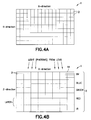
- FIGS. 4A , 4 B and 4 C are a simplified enlarged top view, cross-sectional view and elevational view, respectively, of a light sensor in accordance with the exemplary aspects of this invention.
- FIG. 5 depicts one suitable and non-limiting type of circuitry to implement the receptors of the light sensor of FIG. 4 .
- FIG. 6 shows a block diagram of a device that may be constructed to include the image sensor in accordance with the exemplary embodiments of this invention.
- FIGS. 7A and 7B are each a partial cross-sectional view of the image sensor of FIG. 4 , where in FIG. 7A there is shown one exemplary embodiment where the receptor surface connections are optimized according to the chief ray angle (CRA), and where in FIG. 7B there is shown another exemplary embodiment wherein the receptor layers are shifted by an amount that is a function of the CRA.
- CRA chief ray angle
- FIG. 8 is a graph that plots data element exposure versus exposure time (both in arbitrary units), and is useful in understanding the operation of the image sensor shown in FIG. 4 .
- FIG. 9 is a logic flow diagram that is descriptive of the operation of a method, as well as the execution of computer program instructions, in accordance with exemplary embodiments of this invention.
- the exemplary embodiments of this invention relate at least in part to imaging sensor technology, such as technologies used in color cameras.
- imaging sensor technology such as technologies used in color cameras.
- some current color camera sensors are implemented by using two dimensional pixel arrays that measure light levels by storing charges generated by incoming light.
- a color filter array disposed between the pixel array and the incoming light enables the pixel array to detect color.
- the stored charges may be digitized by using floating diffusion and analog to digital converter (ADC) circuitry.
- ADC analog to digital converter
- the color accuracy may be less than optimum because, typically, only three different color filters are used.
- increasing the number of color filters decreases the resolution.
- color filters can reduce the sensitivity of the sensor since there are optical losses in the filters, resulting in a loss of photons that are not available for imaging purposes.
- Storage space for charge is also problematic, since a small area can only store some maximum amount of photo-induced charge, thereby reducing the dynamic range of the detected pixel values.
- the manufacturing yield of the camera sensors can also be problematic, since the presence of some number of defective pixels may result in image degradation.
- the exemplary embodiments of this invention provide a light sensor (sensor array) 1 that contains a large number of 1-bit light receptors 2 that are arranged as a three dimensional array of light sensors.
- the three dimensional array is organized as i light receptors 2 along an x-axis of the array, j light receptors 2 along a y-axis of the array, and k light receptors 2 along a z-axis of the array, where i may or may not be equal to j, and where i and j may each be much larger than k.
- the k 1-bit light receptors 2 can be seen to be vertically stacked from a light receiving surface 1 A of the sensor 1 into a depth of a substrate 3 , which may be a silicon substrate. Due to the wavelength-dependent absorption coefficient of silicon, the deeper into the substrate 3 that a particular light receptor 2 is located (i.e., the further that it is located from the light receiving surface 1 A) the longer is the wavelength of light that reaches it and that may be absorbed and detected.
- the sensor 1 may be responsive to electromagnetic radiation in the wavelength range that extends from the ultraviolet (UV) to the infrared (IR), and thus may encompass wavelengths in a range from about 4 ⁇ 10 ⁇ 7 m (and shorter) to about 7 ⁇ 10 ⁇ 7 m (and longer).
- An optional lens (not shown in FIG. 4 ) may be disposed between the light receiving surface 1 A and the scene being imaged.
- the binary value of a particular receptor 2 indicates the state of the receptor (on or off).
- a scene viewed by the sensor array 1 is converted to an image, which may be a color image, by processing detected receptor values and calculating the image (resolution and colors) based on those receptor values.
- the x and y dimensions of the receptors 2 in a particular layer of receptors correspond to a specific range of incoming wavelength, thus creating a layer of receptors sensitive to specific color range.
- the z dimension corresponds to a plurality of the receptor layers disposed one above another. There may also be multiple similar layers.
- i and j may both have a value of about 10 6
- k may have a value of about 10 2 or less
- each receptor 2 is capable of storing a 1-bit value (0 or 1).
- the wavelength of incident light defines how deeply the light travels into the sensor 1 .
- the direction at which the light arrives is assumed to be within a field of view (FOV) of the sensor 1 .
- each receptor 2 may have a basically cubic shape (each face is approximately square), and each receptor 2 may have about the same dimensions.
- the shape of the receptors 2 may approximate a three-dimensional rectangular structure, such as are shown in FIG. 4 . It may be beneficial in some embodiments that the receptors 2 that are farther from the light receiving surface 1 A are thicker than (have a greater extent in the z axis) those receptors 2 that are closer to the light receiving surface 1 A. It may also be beneficial in some embodiments that the receptors 2 in a center region of the sensor 1 be smaller than the receptors 2 nearer to the edges (those receptors at or near the image borders).
- FIGS. 7A and 7B are each a partial cross-sectional view of the image sensor of FIG. 4 , where in FIG. 7A there is shown one exemplary embodiment where the receptor surface connections are optimized according to the chief ray angle (CRA), and where in FIG. 7B there is shown another exemplary embodiment wherein the receptor layers are shifted (laterally offset) according to the CRA.
- the chief ray in an optical system is the meridional ray that starts at the edge of the object, and passes through the center of the aperture stop. This ray crosses the optical axis at the locations of the pupils.
- chief rays may be considered to be equivalent to the rays in a pinhole camera.
- the distance between the chief ray and the optical axis at an image location defines the size of the image.
- the top surface (light receiving surface 1 A) connections or contacts 1 C to the receptors 2 in the various layers may be made using vias 1 B (only a few of which are shown).
- the top surface placement of the contacts 1 C may be made in an optimized manner with respect to the CRA, in this case by concentrating the contacts 1 C near the periphery of the light receiving surface 1 A.
- FIG. 7B the receptors 2 of a given layer are shifted laterally with respect to the receptors 2 in other layers, again in accordance with the CRA. Note that while the receptors 2 in adjacent layers in FIG.
- 7A are also shown as being shifted laterally, in other embodiments they may be also arranged so as to directly underlie one another (i.e., to be vertically registered one with another). Note further that in some embodiments the receptors 2 in only some layers may be shifted laterally between layers, while in other layers the receptors may underlie one another and be registered vertically, such as is shown in FIGS. 4A and 4B .
- the thickness of the layers is defined based on the light absorption properties within the material of the sensor 1 (e.g., silicon) and the desired accuracy of detection at different wavelengths.
- One non-limiting approach is to make the thickness of the receptors 2 (and/or the number k of the z-axis receptors) spatially varying (e.g., the center area may contain more and thinner receptors 2 along the z-axis than at the edge/corner areas of the sensor 1 ).
- the receptors 2 may have different sizes in different layers (e.g., see FIGS. 4B , 7 A and 7 B).
- the green light absorbing layer that layer that absorbs wavelengths of visible green color
- the red, blue or IR responsive layers may use more (and physically smaller) receptors 2 than the red, blue or IR responsive layers.
- the individual receptors 2 of the sensor array 1 are reset to a known state (0 or 1).
- a known state (0 or 1).
- the sensor array 2 When light impinges on the sensor array 1 it is absorbed (selectively in depth as a function of wavelength as shown in FIGS. 1 and 3 ) by certain ones of the receptors 2 and changes the state of those receptors (1 or 0).
- the sensor array 2 After some time period the sensor array 2 has captured a large number of photons and some possibly correspondingly large number of receptors 2 have experienced a change of state.
- the probability that a photon will impinge on a receptor that is still in the reset state decreases.
- This type of nonlinear behavior may be taken into account when the receptor (pixel) values are subsequently processed.
- Reference in this regard may be made to the non-limiting example of FIG. 8 , where it may be seen that as the exposure time increases the number of receptors 2 (which may be referred to as “data elements”) asymptotically approaches some maximum value. After some desired exposure period the values of the receptors 2 are read out.
- a three-dimensional image may then be processed into a color image with a desired resolution and color accuracy by combining the bit values in different directions (resolution in the x and y axes) and colors in the z-axis. Dynamics of the processed image are based on the amount of combined receptor values from different directions (and noise).
- the exposure time of the sensor 1 may be based on previously captured image(s). It is also within the scope of the exemplary embodiments, if there is some mechanism in place that enables one to determine a number of receptors 2 that have changed state, to terminate the exposure after some threshold number of receptors 2 have changed state (e.g., 15%). This mechanism may be based on performing multiple successive non-destructive read cycles of the sensor 1 , and continuing until some threshold number of receptors 2 has changed state.
- the senor 1 is wavelength (color) responsive, and thus finds utility as a color imager or a spectral imager, it may be used as well to create black and white and monochrome images. If the amount of incident light is small it may be beneficial to process only reduced resolution luminance information from the sensor 1 . When the scene is lighter then the resolution, and also color accuracy, may be increased.
- the senor 1 it is within the scope of these exemplary embodiments to design the sensor 1 so that it captures different wavelengths of light in different layers, e.g., the top-most layer(s) may capture UV light, the next layers capture visible light and the bottom-most layers capture IR light. All or some of these layers may be used when forming the output image or for detection purposes.
- the outputs of the receptors 2 may be combined both laterally (within a layer) and vertically (between two or more layers).
- Receptors 2 along the x-direction are used for x-resolution, receptors 2 along the y-direction for y-resolution, and receptors 2 along the z-direction for color accuracy.
- a plurality of adjacent receptors 2 may be grouped together to form a single image pixel, and the number of receptors in a particular group may change from exposure to exposure, and the number may be different for different groups during a single exposure. For example, there may be fewer receptors 2 per group towards the center of the light receiving surface 2 A and more receptors 2 per group at the edges of the light receiving surface 2 A.
- the sensor 1 having nine layers, with the read-out receptor values along the z-axis being 1 1 0 0 0 1 1 1 1 from bottom to top.
- the read-out receptor values along the z-axis being 1 1 0 0 0 1 1 1 from bottom to top.
- the sensor 1 be capable of combining bit elements (individual data values) as data elements (combined data values).
- the data that is read out from the digital sensor 1 may be either bit-valued (binary) data or multi-valued data elements.
- the 16 ⁇ 16 ⁇ 9 volume can enable 10-bit dynamic resolution for G, 9 bit dynamic resolution for R, and 9.5 bit dynamic resolution for B.
- the dynamic resolution is still only 8-bit for each color due to the use of the 16 ⁇ 16 volume (in this non-limiting example).
- other combinations are possible since some layers may be used for UV and/or IR detection.
- the sensor 1 may be used for other purposes than for image capture. For example, distance may be based on the detection of the bottom-most (e.g., the IR) layer. In this case assume a presence of an IR light source at a device that includes the sensor 1 (e.g. a camera). The time difference between when the IR light source is activated and when IR light reflected from an object is measured. The distance to the object can thus be determined as being based on half of the round trip travel time of the IR light. This type of measurement system may be used, for example, to assist auto-focus (AF) functionality during image capture.
- AF auto-focus
- the array of receptors 2 may be read, for example, by using technology similar to that found in random access memory, such as dynamic random access memory (DRAM). That is, the sensor 1 may be viewed as representing an array of i ⁇ j ⁇ k addressable one bit storage locations (see also FIG. 4C ). The sensor 1 may be configured such that the receptor values are always reset during a read cycle, or it may be configured that the reset operation is performed separate from the read operation.
- DRAM dynamic random access memory
- the electrical connections are shown for convenience as being made to the vertical sides of the substrate 3 , and not by way of limitation.
- each individual receptor may be designed to have minimal complexity, thereby enabling the sensor 1 to be manufactured with increased yield as compared to conventional sensor arrays.
- Any defective receptors 2 e.g., those with stuck at zero or stuck at one faults, may be identified and their locations mapped and compensated for (such as by using interpolation from adjacent operational receptors 2 ) during image processing.
- the electrical contacts and related circuitry may be either on the top of the sensor array 1 or, possibly more preferably, at the bottom of the sensor array 1 (backside contact). Alternatively, some receptors 2 may be contacted from the top of the sensor array 1 while others may be contacted from the bottom of the sensor array 1 .
- FIG. 4C shows the sensor array 1 with exemplary x-y-z address generation circuitry 4 and receptor (pixel) readout circuitry 5 .
- the receptor readout circuitry 5 receives from the sensor array 1 a stream or streams of essentially binary data (one and zeros) corresponding to those receptors 2 that are turned on (i.e., that have absorbed at least one photon) and those receptors 2 that have not turned on (i.e., are still in the reset state by virtue of not having absorbed at least one photon, or some threshold number of photons).
- the receptor readout circuitry 5 may also be responsible for grouping together the outputs of light receptors into x-y and/or z-axis light receptor groups or neighborhoods.
- the receptor readout circuitry 5 may include a compression function (any suitable compression function may be used, such as run-length encoding), or there may be a separate compression function prior to storage of the readout receptor values.
- the address generation circuitry 4 may generate, at any given time, addresses to readout the receptors 2 layer-wise (row-by-row) or vertically column-by-column.
- the receptor circuitry need not be as complex as that found in many conventional CMOS/CCD sensors, as there is no need to measure floating diffusion current/voltage with an A/D converter. Instead, it is only needed to measure that a particular receptor 2 (pixel) is on or off. Multiple p-n and n-p junctions may be used, but other alternatives can also be used. Also the size of a p-well or n-well (or the substrate) can be much smaller than in conventional CMOS/CCD sensors, since there is no need to store a large amount of charge.
- each receptor 2 includes a photodiode 2 A connected with a simple inverter-based comparator circuit 2 B for one-bit amplitude quantification.
- An adjustable threshold current may be used to prevent triggering due to background illumination.
- a receptor (pixel) is triggered when the signal current (plus background current) exceeds the threshold current I t , and the voltage U in across C pix due to the discharging current I s +I b ⁇ I t goes below the threshold voltage ( ⁇ U dd /2) of the comparator 2 B.
- the sensitivity of a pixel is determined by the optical energy E pix needed for discharging the input capacitance of a pixel: E pix ⁇ ( C pix ⁇ U )/ SK F , where C pix is the total input capacitance of a pixel, comprising the photodiode and circuit input capacitances, ⁇ U is the voltage change at the input needed to trigger the comparator 2 B, S is the photodiode responsivity and KF the pixel fill factor.
- the substrate 3 can be composed of a different materials selected for being responsive to different wavelength bands.
- the visible light detection portion may be comprised of Si
- a UV light detection portion if present
- a Group III-V material such as GaN or AlGaN, or another material such as SiC, as a few non-limiting examples.
- the visible light detection portion may be comprised of Si
- an IR light detection portion if present
- Si may also be IR responsive.
- the exemplary embodiments of this invention to selectively vary at least one dimension, such as the dimension along the z-axis, of the receptors 2 in different layers so as to enhance there responsivity to the wavelength(s) of light to be detected in a particular layer.
- the at least one dimension may be made some fraction of a wavelength, thereby wavelength tuning the receptors 2 in that layer.
- the dimensions of the receptors in the x and y axes may be, for example, in the range of about 0.1 to about 0.2 micrometers, while the thicknesses may vary depending upon the wavelength range that is detected in the corresponding layer of the sensor 1 and possibly also the desired color accuracy and number of layers.
- the actual minimum dimensions of a receptor 2 may be assumed to depend at least in part on the specifics of the fabrication process, such as the wavelengths used for photolithography and similar process-dependent parameters.
- the dimensions and distributions of the receptors 2 may be made a function of the sensor/device geometry, and may be based on a consideration of the chief ray angle (CRA).
- CRA chief ray angle
- the fabrication of the sensor array 1 may be accomplished by any suitable techniques, including one or more of forming multiple implanted/diffused p-n/n-p junctions, by the use of multiple epitaxy/pattern/planarize processing steps to form the individual layers superimposed one above another, and by the use of wafer bonding processing (as non-limiting examples).
- Other technologies may also be used, such as through silicon via (TSV) or through silicon stacking (TSS) technology, to provide for vertically stacking substrates/wafers containing the receptors 2 .
- FIG. 6 illustrates an exemplary embodiment of a device, such as user equipment (UE) 10 , in both plan view (left) and sectional view (right).
- the UE 10 has a graphical display interface 20 and a user interface 22 illustrated as a keypad but understood as also encompassing touch screen technology at the graphical display interface 20 and voice recognition technology received at the microphone 24 .
- a power actuator 26 controls the device being turned on and off by the user.
- the exemplary UE 10 includes a camera 28 which is shown as being forward facing (e.g., for video calls) but may alternatively or additionally be rearward facing (e.g., for capturing images and video for local storage).
- the camera 28 is controlled by a shutter actuator 30 and optionally by a zoom actuator 30 which may alternatively function as a volume adjustment for the speaker(s) 34 when the camera 28 is not in an active mode.
- the camera 28 may be assumed to include an image sensor array 1 that is constructed and operated in accordance with the exemplary embodiments of this invention, as described in detail above.
- the antennas 36 may be multi-band for use with other radios in the UE.
- the operable ground plane for the antennas 36 is shown by shading as spanning the entire space enclosed by the UE housing though in some embodiments the ground plane may be limited to a smaller area, such as disposed on a printed wiring board on which the power chip 38 is formed.
- the power chip 38 controls power amplification on the channels being transmitted and/or across the antennas that transmit simultaneously where spatial diversity is used, and amplifies the received signals.
- the power chip 38 outputs the amplified received signal to the radio frequency (RF) chip 40 which demodulates and downconverts the signal for baseband processing.
- the baseband (BB) chip 42 detects the signal which is then converted to a bit stream and finally decoded. Similar processing occurs in reverse for signals generated in the apparatus 10 and transmitted from it.
- Signals going to and from the camera 28 may pass through an image/video processor 44 that encodes and decodes the various image frames.
- a separate audio processor 46 may also be present controlling signals to and from the speakers 34 and the microphone 24 .
- the graphical display interface 20 is refreshed from a frame memory 48 as controlled by a user interface chip 50 which may process signals to and from the display interface 20 and/or additionally process user inputs from the keypad 22 and elsewhere.
- the UE 10 may also include one or more secondary radios such as a wireless local area network radio WLAN 37 and a Bluetooth radio 39 , which may incorporate an antenna on the chip or be coupled to an antenna off the chip.
- secondary radios such as a wireless local area network radio WLAN 37 and a Bluetooth radio 39 , which may incorporate an antenna on the chip or be coupled to an antenna off the chip.
- various memories such as random access memory RAM 43 , read only memory ROM 45 , and in some embodiments there may be removable memory such as the illustrated memory card 47 on which the various programs 10 C are stored. All of these components within the UE 10 are normally powered by a portable power supply such as a battery 49 .
- the processors 38 , 40 , 42 , 44 , 46 , 50 may operate in a slave relationship to the main processor 10 A, 12 A, which may then be in a master relationship to them.
- Embodiments of this invention may be disposed across various chips and memories as shown, or disposed within another processor that combines some of the functions described above for FIG. 6 Any or all of these various processors of FIG. 6 access one or more of the various memories, which may be on chip with the processor or separate there from.
- Similar function-specific components that are directed toward communications over a network broader than a piconet may also be disposed in exemplary embodiments of the access node 12 , which may have an array of tower mounted antennas rather than the two shown at FIG. 6 .
- the method includes an operation of illuminating a light receiving surface of substrate comprising a three dimensional array of light receptors, where light receptors disposed in an x-y plane that is closer to the light receiving surface are responsive to light having shorter wavelengths than light receptors disposed in an x-y plane that is further from the light receiving surface, and where each light receptor is configured to output a binary value and to change state between an off-state and an on-state by the absorption of at least one photon.
- Block 9 B there is an operation, performed at the end of an exposure period, of reading out binary values from light receptors disposed in at least two different x-y planes of the three dimensional array.
- illuminating includes a preliminary step of resetting the light receptors to the off-state.
- grouping together groups together the binary outputs of some number of light receptors that are adjacent in the same x-y plane of the three dimensional array, or that groups together the binary outputs of some number of light receptors that are adjacent along a z-axis of the three dimensional array, or that groups together the binary outputs of some number of light receptors that are adjacent in the same x-y plane and along the z-axis of the three dimensional array.
- sensor array sensitivity can be improved, the yield of the image sensors can be improved, color accuracy can be improved, resolution can be improved, and the dynamics of the pixel values can be improved.
- any compromise between resolution and color accuracy can be made dynamically.
- many different optimization possibilities are available due at least to the simplicity of the basic sensor structure.
- the sensor array 1 is easy to use and integrate, since all the receptors 2 provide just values of 0 and 1.
- the various exemplary embodiments may be implemented in hardware or special purpose circuits, software, logic or any combination thereof.
- some aspects may be implemented in hardware, while other aspects may be implemented in firmware or software which may be executed by a controller, microprocessor or other computing device, although the exemplary embodiments of this invention are not limited thereto.
- While various aspects of the exemplary embodiments of this invention may be illustrated and described as block diagrams, schematic diagrams or using some other pictorial representation, it is well understood that these blocks, apparatus, systems, techniques or methods described herein may be implemented in, as non-limiting examples, at least in part as hardware, software, firmware, special purpose circuits or logic, general purpose hardware or controller or other computing devices, or some combination thereof.
- the integrated circuit, or circuits may comprise circuitry (as well as possibly firmware) for embodying at least one or more of a data processor or data processors, a digital signal processor or processors, baseband circuitry and radio frequency circuitry that are configurable so as to operate in accordance with the exemplary embodiments of this invention.
- the exemplary embodiments have been described above in FIG. 6 the context of a wireless communications device such as the UE 10 , it should be appreciated that the exemplary embodiments of this invention are not limited for use with only this one particular type of wireless communication device, and that they may be used to advantage in other types of devices that may or may not have wireless communications capability, including digital cameras, PDAs, computers and gaming devices, as non-limiting examples.
- individual receptors 2 need not be transistor/photodiode based, but may be constructed using other types of devices, including quantum dots and other nanostructure devices.
- the exemplary embodiments of this invention are not to be construed as being limited to any of the specific materials, combinations of materials, fabrication processes, wavelengths and/or dimensions that were mentioned above.
- not all layers of the sensor array 1 need be populated with receptors 2 .
- receptors 2 For example, and assuming a non-limiting case of an application where it was desired to detect only blue light and red light, then only those portions of the substrate 3 receptive to these wavelengths need include receptors 2 , thereby effectively notch filtering out the wavelengths of light that lie between blue and red.
- the same effect may be achieved by providing the sensor array 1 that is responsive to all wavelengths in the range of blue to red, and then only reading out the layer or layers of receptors 2 that are responsive to blue and the layer or layers of receptors 2 that are responsive to red.
- connection means any connection or coupling, either direct or indirect, between two or more elements, and may encompass the presence of one or more intermediate elements between two elements that are “connected” or “coupled” together.
- the coupling or connection between the elements can be physical, logical, or a combination thereof.
- two elements may be considered to be “connected” or “coupled” together by the use of one or more wires, cables and/or printed electrical connections, as well as by the use of electromagnetic energy, such as electromagnetic energy having wavelengths in the radio frequency region, the microwave region and the optical (both visible and invisible) region, as several non-limiting and non-exhaustive examples.
Landscapes
- Physics & Mathematics (AREA)
- Spectroscopy & Molecular Physics (AREA)
- General Physics & Mathematics (AREA)
- Engineering & Computer Science (AREA)
- Multimedia (AREA)
- Signal Processing (AREA)
- Human Computer Interaction (AREA)
- Power Engineering (AREA)
- Solid State Image Pick-Up Elements (AREA)
Priority Applications (10)
| Application Number | Priority Date | Filing Date | Title |
|---|---|---|---|
| US12/384,549 US8816460B2 (en) | 2009-04-06 | 2009-04-06 | Image sensor |
| PCT/FI2010/050065 WO2010116023A1 (en) | 2009-04-06 | 2010-02-04 | Image sensor |
| BRPI1009211A BRPI1009211A2 (pt) | 2009-04-06 | 2010-02-04 | "sensor de imagem" |
| CA2841508A CA2841508C (en) | 2009-04-06 | 2010-02-04 | Three dimensional image sensor array with binary output data |
| KR1020117026314A KR101434014B1 (ko) | 2009-04-06 | 2010-02-04 | 광 검출 장치 및 방법 |
| EP10761224.4A EP2417632B1 (de) | 2009-04-06 | 2010-02-04 | Blldsensor |
| CN201080014897.3A CN102365742B (zh) | 2009-04-06 | 2010-02-04 | 图像传感器 |
| CA2757792A CA2757792C (en) | 2009-04-06 | 2010-02-04 | Three dimensional image sensor array with binary output data |
| TW099110334A TWI556418B (zh) | 2009-04-06 | 2010-04-02 | 影像感測器 |
| US14/328,851 US9257475B2 (en) | 2009-04-06 | 2014-07-11 | Image sensor |
Applications Claiming Priority (1)
| Application Number | Priority Date | Filing Date | Title |
|---|---|---|---|
| US12/384,549 US8816460B2 (en) | 2009-04-06 | 2009-04-06 | Image sensor |
Related Child Applications (1)
| Application Number | Title | Priority Date | Filing Date |
|---|---|---|---|
| US14/328,851 Division US9257475B2 (en) | 2009-04-06 | 2014-07-11 | Image sensor |
Publications (2)
| Publication Number | Publication Date |
|---|---|
| US20100252716A1 US20100252716A1 (en) | 2010-10-07 |
| US8816460B2 true US8816460B2 (en) | 2014-08-26 |
Family
ID=42825405
Family Applications (2)
| Application Number | Title | Priority Date | Filing Date |
|---|---|---|---|
| US12/384,549 Active 2029-12-06 US8816460B2 (en) | 2009-04-06 | 2009-04-06 | Image sensor |
| US14/328,851 Active US9257475B2 (en) | 2009-04-06 | 2014-07-11 | Image sensor |
Family Applications After (1)
| Application Number | Title | Priority Date | Filing Date |
|---|---|---|---|
| US14/328,851 Active US9257475B2 (en) | 2009-04-06 | 2014-07-11 | Image sensor |
Country Status (8)
| Country | Link |
|---|---|
| US (2) | US8816460B2 (de) |
| EP (1) | EP2417632B1 (de) |
| KR (1) | KR101434014B1 (de) |
| CN (1) | CN102365742B (de) |
| BR (1) | BRPI1009211A2 (de) |
| CA (2) | CA2841508C (de) |
| TW (1) | TWI556418B (de) |
| WO (1) | WO2010116023A1 (de) |
Cited By (10)
| Publication number | Priority date | Publication date | Assignee | Title |
|---|---|---|---|---|
| US20120298841A1 (en) * | 2009-12-18 | 2012-11-29 | Canon Kabushiki Kaisha | Solid-state image pickup apparatus |
| US9979907B2 (en) * | 2015-09-18 | 2018-05-22 | Sony Corporation | Multi-layered high-dynamic range sensor |
| US10795168B2 (en) | 2017-08-31 | 2020-10-06 | Metalenz, Inc. | Transmissive metasurface lens integration |
| US11906698B2 (en) | 2017-05-24 | 2024-02-20 | The Trustees Of Columbia University In The City Of New York | Broadband achromatic flat optical components by dispersion-engineered dielectric metasurfaces |
| US11927769B2 (en) | 2022-03-31 | 2024-03-12 | Metalenz, Inc. | Polarization sorting metasurface microlens array device |
| US11978752B2 (en) | 2019-07-26 | 2024-05-07 | Metalenz, Inc. | Aperture-metasurface and hybrid refractive-metasurface imaging systems |
| US12140778B2 (en) | 2018-07-02 | 2024-11-12 | Metalenz, Inc. | Metasurfaces for laser speckle reduction |
| US12416752B2 (en) | 2018-01-24 | 2025-09-16 | President And Fellows Of Harvard College | Polarization state generation with a metasurface |
| US12460919B2 (en) | 2019-10-31 | 2025-11-04 | President And Fellows Of Harvard College | Compact metalens depth sensors |
| US12548980B2 (en) | 2021-05-25 | 2026-02-10 | Metalenz, Inc. | Single element dot pattern projector |
Families Citing this family (11)
| Publication number | Priority date | Publication date | Assignee | Title |
|---|---|---|---|---|
| US8648287B1 (en) | 2005-05-27 | 2014-02-11 | Rambus Inc. | Image sensor using single photon jots and processor to create pixels |
| US8134115B2 (en) * | 2009-06-23 | 2012-03-13 | Nokia Corporation | Color filters for sub-diffraction limit-sized light sensors |
| US8420996B2 (en) * | 2009-12-23 | 2013-04-16 | Nokia Corporation | Intensity estimation using binary sensor array with spatially varying thresholds |
| US8319855B2 (en) * | 2010-01-19 | 2012-11-27 | Rambus Inc. | Method, apparatus and system for image acquisition and conversion |
| KR101565748B1 (ko) | 2013-05-31 | 2015-11-05 | 삼성에스디에스 주식회사 | 이미지에서 반복 패턴을 검출하는 방법 및 장치 |
| US9621864B2 (en) * | 2014-01-14 | 2017-04-11 | Microsoft Technology Licensing, Llc | Spectral imaging system |
| US9752929B2 (en) * | 2014-05-08 | 2017-09-05 | Pinnacle Imaging Corporation | Light-detecting device and method for converting optical radiation on switched conductivity diodes |
| US9865642B2 (en) * | 2015-06-05 | 2018-01-09 | Omnivision Technologies, Inc. | RGB-IR photosensor with nonuniform buried P-well depth profile for reduced cross talk and enhanced infrared sensitivity |
| KR101961439B1 (ko) * | 2018-06-14 | 2019-07-17 | 강용훈 | 센서 유닛 및 이를 포함하는 자외선 검출 장치 |
| JP7242285B2 (ja) * | 2018-12-19 | 2023-03-20 | キオクシア株式会社 | 半導体装置 |
| CN112770020A (zh) | 2019-11-05 | 2021-05-07 | 北京小米移动软件有限公司 | 图像传感模组、方法、装置、电子设备及介质 |
Citations (44)
| Publication number | Priority date | Publication date | Assignee | Title |
|---|---|---|---|---|
| US3981565A (en) | 1972-10-28 | 1976-09-21 | Canon Kabushiki Kaisha | Light-modulating device |
| US4011016A (en) | 1974-04-30 | 1977-03-08 | Martin Marietta Corporation | Semiconductor radiation wavelength detector |
| US5965875A (en) | 1998-04-24 | 1999-10-12 | Foveon, Inc. | Color separation in an active pixel cell imaging array using a triple-well structure |
| US6252577B1 (en) | 1999-03-18 | 2001-06-26 | Intel Corporation | Efficient methodology for scaling and transferring images |
| US20020114526A1 (en) | 2001-02-08 | 2002-08-22 | Stmicroelectronics Ltd. | Reference data coding in solid state image sensors |
| KR20020077793A (ko) | 1999-05-21 | 2002-10-14 | 포베온, 인크. | 이미징 어레이로부터 디지털 이미지 데이터를 저장 및검색하는 방법 |
| US6498576B1 (en) * | 2000-05-09 | 2002-12-24 | Pixim, Inc. | Selective analog-to-digital conversion for a digital pixel sensor |
| US6552746B1 (en) * | 1998-09-22 | 2003-04-22 | Pixim, Inc. | Apparatus having an image sensor that is variable in spatial resolution and bit resolution and associated method |
| US20030209651A1 (en) | 2002-05-08 | 2003-11-13 | Canon Kabushiki Kaisha | Color image pickup device and color light-receiving device |
| WO2004009986A1 (de) | 2002-07-23 | 2004-01-29 | Daimlerchrysler Ag | Druckguss-zylinderkurbelgehäuse |
| US6704046B2 (en) | 2002-04-17 | 2004-03-09 | Motorola, Inc. | Digital pixel image sensor with independent color channel reference signals |
| US6727521B2 (en) | 2000-09-25 | 2004-04-27 | Foveon, Inc. | Vertical color filter detector group and array |
| US20040085468A1 (en) * | 2002-10-30 | 2004-05-06 | Microsoft Corporation | Photo-sensor array with pixel-level signal comparison |
| US20040178465A1 (en) * | 2002-03-20 | 2004-09-16 | Foveon, Inc. | Vertical color filter sensor group with non-sensor filter and method for fabricating such a sensor group |
| US20040218073A1 (en) | 2003-04-30 | 2004-11-04 | Nokia Corporation | Color filter array interpolation |
| WO2004099865A2 (en) | 2003-05-02 | 2004-11-18 | Massachusetts Institute Of Technology | Digital photon-counting geiger-mode avalanche photodiode solid-state monolithic intensity imaging focal-plane with scalable readout circuitry |
| US20040245592A1 (en) | 2003-05-01 | 2004-12-09 | Yale University | Solid state microchannel plate photodetector |
| US6864557B2 (en) | 2001-06-18 | 2005-03-08 | Foveon, Inc. | Vertical color filter detector group and array |
| US6924167B1 (en) | 2002-08-15 | 2005-08-02 | Foveon, Inc. | Method of forming a bandgap tuned vertical color imager cell |
| US20050185075A1 (en) | 1999-08-19 | 2005-08-25 | Dialog Semiconductor Gmbh | Method and apparatus for controlling pixel sensor elements |
| JP2005268384A (ja) | 2004-03-17 | 2005-09-29 | Fuji Photo Film Co Ltd | 光電変換膜積層型固体撮像素子 |
| US6960757B2 (en) | 2001-06-18 | 2005-11-01 | Foveon, Inc. | Simplified wiring schemes for vertical color filter pixel sensors |
| US20060012832A1 (en) | 2004-07-14 | 2006-01-19 | Fuji Photo Film Co., Ltd. | Printer unit and electronic camera |
| US20060033114A1 (en) * | 2004-08-13 | 2006-02-16 | Schranz Paul S | Light emitting and imaging sensing device and apparatus |
| US20060054782A1 (en) | 2004-08-25 | 2006-03-16 | Olsen Richard I | Apparatus for multiple camera devices and method of operating same |
| EP1667246A1 (de) | 2004-12-03 | 2006-06-07 | ETeCH AG | Mehrfarbenempfindliches Bauteil zur Farbbilderfassung |
| US20060124832A1 (en) | 2004-09-27 | 2006-06-15 | Lightspin Technologies, Inc. | Wide dynamic range photodetector |
| US7166880B2 (en) | 2002-03-20 | 2007-01-23 | Foveon, Inc. | Vertical color filter sensor group with carrier-collection elements of different size and method for fabricating such a sensor group |
| US20070045685A1 (en) | 2005-08-24 | 2007-03-01 | Micron Technology, Inc. | Method and apparatus providing integrated color pixel with buried sub-wavelength gratings in solid state imagers |
| US20080011937A1 (en) | 2006-06-30 | 2008-01-17 | Matsushita Electric Industrial Co., Ltd. | Solid-state imaging element and solid-state imaging device |
| WO2008067472A2 (en) | 2006-11-29 | 2008-06-05 | President And Fellows Of Harvard College | A new spatio-spectral sampling paradigm for imaging and a novel color filter array design |
| US20080128698A1 (en) | 2002-02-05 | 2008-06-05 | Peter Martin | Many million pixel image sensor |
| WO2008082569A1 (en) | 2006-12-29 | 2008-07-10 | Nanolambda, Inc. | Wavelength selective metallic embossing nanostructure |
| WO2008131313A2 (en) | 2007-04-18 | 2008-10-30 | Invisage Technologies, Inc. | Materials systems and methods for optoelectronic devices |
| KR100875140B1 (ko) | 2007-11-01 | 2008-12-22 | 실리콤텍(주) | 기준전압이 자동으로 조절되는 저전력 이미지 센서 및 이이미지 센서가 포함되어 하나의 칩 상에 집적된 집적회로 |
| US20090251581A1 (en) | 2008-04-08 | 2009-10-08 | Samsung Electronics Co., Ltd. | Sub-pixels, unit pixels, image sensors and methods of operating the same |
| WO2009136989A1 (en) | 2008-05-09 | 2009-11-12 | Ecole Polytechnique Federale De Lausanne | Image sensor having nonlinear response |
| EP2149904A2 (de) | 2008-07-28 | 2010-02-03 | Ricoh Company, Limited | Abbildungsvorrichtung |
| US20100033604A1 (en) | 2006-07-11 | 2010-02-11 | Neal Solomon | Digital imaging system for correcting image aberrations |
| US20100073294A1 (en) | 2006-11-17 | 2010-03-25 | Silicon Communications Technology Co., Ltd. | Low power image sensor adjusting reference voltage automatically and optical pointing device comprising the same |
| US20100321542A1 (en) | 2009-06-23 | 2010-12-23 | Nokia Corporation | Gradient color filters for sub-diffraction limit sensors |
| US20100320369A1 (en) | 2009-06-23 | 2010-12-23 | Nokia Corporation | Color filters for sub-diffraction limit sensors |
| US20100320368A1 (en) | 2009-06-23 | 2010-12-23 | Nokia Corporation | Color filters for sub-diffraction limit sensors |
| US7916193B2 (en) | 1998-02-23 | 2011-03-29 | Round Rock Research, Llc | Interpolator for a CMOS image sensor using a digital register |
Family Cites Families (3)
| Publication number | Priority date | Publication date | Assignee | Title |
|---|---|---|---|---|
| US7408572B2 (en) * | 2002-07-06 | 2008-08-05 | Nova Research, Inc. | Method and apparatus for an on-chip variable acuity imager array incorporating roll, pitch and yaw angle rates measurement |
| WO2004015764A2 (en) * | 2002-08-08 | 2004-02-19 | Leedy Glenn J | Vertical system integration |
| JP4907557B2 (ja) * | 2006-01-25 | 2012-03-28 | 京セラ株式会社 | 撮像素子及びカメラモジュール |
-
2009
- 2009-04-06 US US12/384,549 patent/US8816460B2/en active Active
-
2010
- 2010-02-04 BR BRPI1009211A patent/BRPI1009211A2/pt not_active Application Discontinuation
- 2010-02-04 KR KR1020117026314A patent/KR101434014B1/ko active Active
- 2010-02-04 CN CN201080014897.3A patent/CN102365742B/zh active Active
- 2010-02-04 CA CA2841508A patent/CA2841508C/en active Active
- 2010-02-04 CA CA2757792A patent/CA2757792C/en active Active
- 2010-02-04 EP EP10761224.4A patent/EP2417632B1/de active Active
- 2010-02-04 WO PCT/FI2010/050065 patent/WO2010116023A1/en not_active Ceased
- 2010-04-02 TW TW099110334A patent/TWI556418B/zh active
-
2014
- 2014-07-11 US US14/328,851 patent/US9257475B2/en active Active
Patent Citations (46)
| Publication number | Priority date | Publication date | Assignee | Title |
|---|---|---|---|---|
| US3981565A (en) | 1972-10-28 | 1976-09-21 | Canon Kabushiki Kaisha | Light-modulating device |
| US4011016A (en) | 1974-04-30 | 1977-03-08 | Martin Marietta Corporation | Semiconductor radiation wavelength detector |
| US7916193B2 (en) | 1998-02-23 | 2011-03-29 | Round Rock Research, Llc | Interpolator for a CMOS image sensor using a digital register |
| US5965875A (en) | 1998-04-24 | 1999-10-12 | Foveon, Inc. | Color separation in an active pixel cell imaging array using a triple-well structure |
| US6552746B1 (en) * | 1998-09-22 | 2003-04-22 | Pixim, Inc. | Apparatus having an image sensor that is variable in spatial resolution and bit resolution and associated method |
| US6252577B1 (en) | 1999-03-18 | 2001-06-26 | Intel Corporation | Efficient methodology for scaling and transferring images |
| KR20020077793A (ko) | 1999-05-21 | 2002-10-14 | 포베온, 인크. | 이미징 어레이로부터 디지털 이미지 데이터를 저장 및검색하는 방법 |
| US20020171881A1 (en) * | 1999-05-21 | 2002-11-21 | Foveon, Inc., A California Corporation. | Vertical color filter detector and array method for storing and retrieving digital image data from an imaging array |
| US20050185075A1 (en) | 1999-08-19 | 2005-08-25 | Dialog Semiconductor Gmbh | Method and apparatus for controlling pixel sensor elements |
| US6498576B1 (en) * | 2000-05-09 | 2002-12-24 | Pixim, Inc. | Selective analog-to-digital conversion for a digital pixel sensor |
| US6727521B2 (en) | 2000-09-25 | 2004-04-27 | Foveon, Inc. | Vertical color filter detector group and array |
| US20020114526A1 (en) | 2001-02-08 | 2002-08-22 | Stmicroelectronics Ltd. | Reference data coding in solid state image sensors |
| US6864557B2 (en) | 2001-06-18 | 2005-03-08 | Foveon, Inc. | Vertical color filter detector group and array |
| US6960757B2 (en) | 2001-06-18 | 2005-11-01 | Foveon, Inc. | Simplified wiring schemes for vertical color filter pixel sensors |
| US20080128698A1 (en) | 2002-02-05 | 2008-06-05 | Peter Martin | Many million pixel image sensor |
| US7166880B2 (en) | 2002-03-20 | 2007-01-23 | Foveon, Inc. | Vertical color filter sensor group with carrier-collection elements of different size and method for fabricating such a sensor group |
| US20040178465A1 (en) * | 2002-03-20 | 2004-09-16 | Foveon, Inc. | Vertical color filter sensor group with non-sensor filter and method for fabricating such a sensor group |
| US6704046B2 (en) | 2002-04-17 | 2004-03-09 | Motorola, Inc. | Digital pixel image sensor with independent color channel reference signals |
| US20030209651A1 (en) | 2002-05-08 | 2003-11-13 | Canon Kabushiki Kaisha | Color image pickup device and color light-receiving device |
| WO2004009986A1 (de) | 2002-07-23 | 2004-01-29 | Daimlerchrysler Ag | Druckguss-zylinderkurbelgehäuse |
| US6924167B1 (en) | 2002-08-15 | 2005-08-02 | Foveon, Inc. | Method of forming a bandgap tuned vertical color imager cell |
| US20040085468A1 (en) * | 2002-10-30 | 2004-05-06 | Microsoft Corporation | Photo-sensor array with pixel-level signal comparison |
| US20040218073A1 (en) | 2003-04-30 | 2004-11-04 | Nokia Corporation | Color filter array interpolation |
| US20040245592A1 (en) | 2003-05-01 | 2004-12-09 | Yale University | Solid state microchannel plate photodetector |
| WO2004099865A2 (en) | 2003-05-02 | 2004-11-18 | Massachusetts Institute Of Technology | Digital photon-counting geiger-mode avalanche photodiode solid-state monolithic intensity imaging focal-plane with scalable readout circuitry |
| JP2005268384A (ja) | 2004-03-17 | 2005-09-29 | Fuji Photo Film Co Ltd | 光電変換膜積層型固体撮像素子 |
| US20060012832A1 (en) | 2004-07-14 | 2006-01-19 | Fuji Photo Film Co., Ltd. | Printer unit and electronic camera |
| US20060033114A1 (en) * | 2004-08-13 | 2006-02-16 | Schranz Paul S | Light emitting and imaging sensing device and apparatus |
| US20060054782A1 (en) | 2004-08-25 | 2006-03-16 | Olsen Richard I | Apparatus for multiple camera devices and method of operating same |
| US20060124832A1 (en) | 2004-09-27 | 2006-06-15 | Lightspin Technologies, Inc. | Wide dynamic range photodetector |
| EP1667246A1 (de) | 2004-12-03 | 2006-06-07 | ETeCH AG | Mehrfarbenempfindliches Bauteil zur Farbbilderfassung |
| US20070045685A1 (en) | 2005-08-24 | 2007-03-01 | Micron Technology, Inc. | Method and apparatus providing integrated color pixel with buried sub-wavelength gratings in solid state imagers |
| US20080011937A1 (en) | 2006-06-30 | 2008-01-17 | Matsushita Electric Industrial Co., Ltd. | Solid-state imaging element and solid-state imaging device |
| US20100033604A1 (en) | 2006-07-11 | 2010-02-11 | Neal Solomon | Digital imaging system for correcting image aberrations |
| US20100073294A1 (en) | 2006-11-17 | 2010-03-25 | Silicon Communications Technology Co., Ltd. | Low power image sensor adjusting reference voltage automatically and optical pointing device comprising the same |
| WO2008067472A2 (en) | 2006-11-29 | 2008-06-05 | President And Fellows Of Harvard College | A new spatio-spectral sampling paradigm for imaging and a novel color filter array design |
| WO2008082569A1 (en) | 2006-12-29 | 2008-07-10 | Nanolambda, Inc. | Wavelength selective metallic embossing nanostructure |
| US20090152664A1 (en) * | 2007-04-18 | 2009-06-18 | Ethan Jacob Dukenfield Klem | Materials, Systems and Methods for Optoelectronic Devices |
| WO2008131313A2 (en) | 2007-04-18 | 2008-10-30 | Invisage Technologies, Inc. | Materials systems and methods for optoelectronic devices |
| KR100875140B1 (ko) | 2007-11-01 | 2008-12-22 | 실리콤텍(주) | 기준전압이 자동으로 조절되는 저전력 이미지 센서 및 이이미지 센서가 포함되어 하나의 칩 상에 집적된 집적회로 |
| US20090251581A1 (en) | 2008-04-08 | 2009-10-08 | Samsung Electronics Co., Ltd. | Sub-pixels, unit pixels, image sensors and methods of operating the same |
| WO2009136989A1 (en) | 2008-05-09 | 2009-11-12 | Ecole Polytechnique Federale De Lausanne | Image sensor having nonlinear response |
| EP2149904A2 (de) | 2008-07-28 | 2010-02-03 | Ricoh Company, Limited | Abbildungsvorrichtung |
| US20100321542A1 (en) | 2009-06-23 | 2010-12-23 | Nokia Corporation | Gradient color filters for sub-diffraction limit sensors |
| US20100320369A1 (en) | 2009-06-23 | 2010-12-23 | Nokia Corporation | Color filters for sub-diffraction limit sensors |
| US20100320368A1 (en) | 2009-06-23 | 2010-12-23 | Nokia Corporation | Color filters for sub-diffraction limit sensors |
Non-Patent Citations (9)
| Title |
|---|
| "Bayer filter", http://en.wikipedia.org/wiki/Bayer-filter, May 15, 2009, 4 pgs. |
| "Bayer filter", http://en.wikipedia.org/wiki/Bayer—filter, May 15, 2009, 4 pgs. |
| "Digital optical position-sensitive detector (PSD)", Anssi Makynen, et al., IMTC 2004-Instrumentation and Measurement, IEEE 2004, pp. 2358-2360. |
| "Digital optical position-sensitive detector (PSD)", Anssi Makynen, et al., IMTC 2004—Instrumentation and Measurement, IEEE 2004, pp. 2358-2360. |
| "Foveon X3 sensor", http://en.wikipedia.org/wiki/Foveon-X3-sensor , May 15, 2009. |
| "Foveon X3 sensor", http://en.wikipedia.org/wiki/Foveon—X3—sensor , May 15, 2009. |
| E. Fossum, "Gigapixel Digital Film Sensor (DFS) Proposal", Nanospace Manipulation of Photons and Electrons for Nanovision Systems, Oct. 25-26, 2005. |
| Gigapixel Digital Film Sensor (DFS) Proposal, Eric R. Fossum, 7th Takayanagi Kenjiro Memorial Symposium and the 2nd International Symposium on Nanovision Science, University of Shizuoka, Oct. 2005, 5 pgs. |
| L. Sbaiz, et al, "The Gigavision Camera", IEEE International Conference on Acoustics, Speech and Signal Processing 2009, pp. 1093-1096, Apr. 19-24, 2009. |
Cited By (18)
| Publication number | Priority date | Publication date | Assignee | Title |
|---|---|---|---|---|
| US20120298841A1 (en) * | 2009-12-18 | 2012-11-29 | Canon Kabushiki Kaisha | Solid-state image pickup apparatus |
| US9245919B2 (en) * | 2009-12-18 | 2016-01-26 | Canon Kabushiki Kaisha | Solid-state image pickup apparatus |
| US20160104728A1 (en) * | 2009-12-18 | 2016-04-14 | Canon Kabushiki Kaisha | Solid-state image pickup apparatus |
| US9865631B2 (en) * | 2009-12-18 | 2018-01-09 | Canon Kabushiki Kaisha | Solid-state image pickup apparatus |
| US9979907B2 (en) * | 2015-09-18 | 2018-05-22 | Sony Corporation | Multi-layered high-dynamic range sensor |
| US11906698B2 (en) | 2017-05-24 | 2024-02-20 | The Trustees Of Columbia University In The City Of New York | Broadband achromatic flat optical components by dispersion-engineered dielectric metasurfaces |
| US10795168B2 (en) | 2017-08-31 | 2020-10-06 | Metalenz, Inc. | Transmissive metasurface lens integration |
| US11579456B2 (en) | 2017-08-31 | 2023-02-14 | Metalenz, Inc. | Transmissive metasurface lens integration |
| US11988844B2 (en) | 2017-08-31 | 2024-05-21 | Metalenz, Inc. | Transmissive metasurface lens integration |
| US12411348B2 (en) | 2017-08-31 | 2025-09-09 | Metalenz, Inc. | Transmissive metasurface lens integration |
| US12416752B2 (en) | 2018-01-24 | 2025-09-16 | President And Fellows Of Harvard College | Polarization state generation with a metasurface |
| US12140778B2 (en) | 2018-07-02 | 2024-11-12 | Metalenz, Inc. | Metasurfaces for laser speckle reduction |
| US11978752B2 (en) | 2019-07-26 | 2024-05-07 | Metalenz, Inc. | Aperture-metasurface and hybrid refractive-metasurface imaging systems |
| US12389700B2 (en) | 2019-07-26 | 2025-08-12 | Metalenz, Inc. | Aperture-metasurface and hybrid refractive-metasurface imaging systems |
| US12460919B2 (en) | 2019-10-31 | 2025-11-04 | President And Fellows Of Harvard College | Compact metalens depth sensors |
| US12548980B2 (en) | 2021-05-25 | 2026-02-10 | Metalenz, Inc. | Single element dot pattern projector |
| US11927769B2 (en) | 2022-03-31 | 2024-03-12 | Metalenz, Inc. | Polarization sorting metasurface microlens array device |
| US12276807B2 (en) | 2022-03-31 | 2025-04-15 | Metalenz, Inc. | Polarization sorting metasurface microlens array device |
Also Published As
| Publication number | Publication date |
|---|---|
| CA2757792A1 (en) | 2010-10-14 |
| TW201119018A (en) | 2011-06-01 |
| KR20120009481A (ko) | 2012-01-31 |
| US20100252716A1 (en) | 2010-10-07 |
| CA2841508C (en) | 2018-08-07 |
| CA2841508A1 (en) | 2010-10-14 |
| US9257475B2 (en) | 2016-02-09 |
| KR101434014B1 (ko) | 2014-09-22 |
| WO2010116023A1 (en) | 2010-10-14 |
| BRPI1009211A2 (pt) | 2016-03-15 |
| EP2417632A4 (de) | 2016-07-06 |
| EP2417632A1 (de) | 2012-02-15 |
| CN102365742A (zh) | 2012-02-29 |
| TWI556418B (zh) | 2016-11-01 |
| US20140319324A1 (en) | 2014-10-30 |
| CA2757792C (en) | 2016-04-05 |
| EP2417632B1 (de) | 2019-01-09 |
| CN102365742B (zh) | 2014-07-16 |
Similar Documents
| Publication | Publication Date | Title |
|---|---|---|
| US9257475B2 (en) | Image sensor | |
| US8198578B2 (en) | Color filters for sub-diffraction limit-sized light sensors | |
| US8134115B2 (en) | Color filters for sub-diffraction limit-sized light sensors | |
| US8179457B2 (en) | Gradient color filters for sub-diffraction limit sensors | |
| CN105493285B (zh) | 固态成像器件及电子设备 | |
| CN102339839B (zh) | 具有改良的光电二极管区域分配的cmos图像传感器 | |
| US9683890B2 (en) | Image sensor pixels with conductive bias grids | |
| CN212323001U (zh) | 图像传感器像素和图像传感器像素阵列 | |
| US20210280623A1 (en) | Phase detection pixels with stacked microlenses | |
| US20210280624A1 (en) | Imaging systems with improved microlenses for enhanced near-infrared detection | |
| CN120786967A (zh) | 堆叠硅光电倍增器 |
Legal Events
| Date | Code | Title | Description |
|---|---|---|---|
| AS | Assignment |
Owner name: NOKIA CORPORATION, FINLAND Free format text: ASSIGNMENT OF ASSIGNORS INTEREST;ASSIGNORS:KALEVO, OSSI M.;KOSKINEN, SAMU T.;RISSA, TERO;REEL/FRAME:022533/0759 Effective date: 20090402 |
|
| FEPP | Fee payment procedure |
Free format text: PAYOR NUMBER ASSIGNED (ORIGINAL EVENT CODE: ASPN); ENTITY STATUS OF PATENT OWNER: LARGE ENTITY |
|
| STCF | Information on status: patent grant |
Free format text: PATENTED CASE |
|
| AS | Assignment |
Owner name: NOKIA TECHNOLOGIES OY, FINLAND Free format text: ASSIGNMENT OF ASSIGNORS INTEREST;ASSIGNOR:NOKIA CORPORATION;REEL/FRAME:035280/0093 Effective date: 20150116 |
|
| MAFP | Maintenance fee payment |
Free format text: PAYMENT OF MAINTENANCE FEE, 4TH YEAR, LARGE ENTITY (ORIGINAL EVENT CODE: M1551) Year of fee payment: 4 |
|
| MAFP | Maintenance fee payment |
Free format text: PAYMENT OF MAINTENANCE FEE, 8TH YEAR, LARGE ENTITY (ORIGINAL EVENT CODE: M1552); ENTITY STATUS OF PATENT OWNER: LARGE ENTITY Year of fee payment: 8 |
|
| MAFP | Maintenance fee payment |
Free format text: PAYMENT OF MAINTENANCE FEE, 12TH YEAR, LARGE ENTITY (ORIGINAL EVENT CODE: M1553); ENTITY STATUS OF PATENT OWNER: LARGE ENTITY Year of fee payment: 12 |