US8780678B2 - Thermal-assisted-magnetic-recording head having core cover layer - Google Patents
Thermal-assisted-magnetic-recording head having core cover layer Download PDFInfo
- Publication number
- US8780678B2 US8780678B2 US13/392,115 US201113392115A US8780678B2 US 8780678 B2 US8780678 B2 US 8780678B2 US 201113392115 A US201113392115 A US 201113392115A US 8780678 B2 US8780678 B2 US 8780678B2
- Authority
- US
- United States
- Prior art keywords
- core
- magnetic
- light
- thickness
- spot size
- Prior art date
- Legal status (The legal status is an assumption and is not a legal conclusion. Google has not performed a legal analysis and makes no representation as to the accuracy of the status listed.)
- Expired - Fee Related
Links
Images


Classifications
-
- G—PHYSICS
- G11—INFORMATION STORAGE
- G11B—INFORMATION STORAGE BASED ON RELATIVE MOVEMENT BETWEEN RECORD CARRIER AND TRANSDUCER
- G11B5/00—Recording by magnetisation or demagnetisation of a record carrier; Reproducing by magnetic means; Record carriers therefor
- G11B5/127—Structure or manufacture of heads, e.g. inductive
- G11B5/31—Structure or manufacture of heads, e.g. inductive using thin films
- G11B5/3109—Details
- G11B5/313—Disposition of layers
- G11B5/3133—Disposition of layers including layers not usually being a part of the electromagnetic transducer structure and providing additional features, e.g. for improving heat radiation, reduction of power dissipation, adaptations for measurement or indication of gap depth or other properties of the structure
- G11B5/314—Disposition of layers including layers not usually being a part of the electromagnetic transducer structure and providing additional features, e.g. for improving heat radiation, reduction of power dissipation, adaptations for measurement or indication of gap depth or other properties of the structure where the layers are extra layers normally not provided in the transducing structure, e.g. optical layers
-
- G—PHYSICS
- G11—INFORMATION STORAGE
- G11B—INFORMATION STORAGE BASED ON RELATIVE MOVEMENT BETWEEN RECORD CARRIER AND TRANSDUCER
- G11B5/00—Recording by magnetisation or demagnetisation of a record carrier; Reproducing by magnetic means; Record carriers therefor
- G11B5/48—Disposition or mounting of heads or head supports relative to record carriers ; arrangements of heads, e.g. for scanning the record carrier to increase the relative speed
- G11B5/58—Disposition or mounting of heads or head supports relative to record carriers ; arrangements of heads, e.g. for scanning the record carrier to increase the relative speed with provision for moving the head for the purpose of maintaining alignment of the head relative to the record carrier during transducing operation, e.g. to compensate for surface irregularities of the latter or for track following
- G11B5/60—Fluid-dynamic spacing of heads from record-carriers
- G11B5/6005—Specially adapted for spacing from a rotating disc using a fluid cushion
- G11B5/6088—Optical waveguide in or on flying head
-
- G—PHYSICS
- G11—INFORMATION STORAGE
- G11B—INFORMATION STORAGE BASED ON RELATIVE MOVEMENT BETWEEN RECORD CARRIER AND TRANSDUCER
- G11B5/00—Recording by magnetisation or demagnetisation of a record carrier; Reproducing by magnetic means; Record carriers therefor
- G11B2005/0002—Special dispositions or recording techniques
- G11B2005/0005—Arrangements, methods or circuits
- G11B2005/001—Controlling recording characteristics of record carriers or transducing characteristics of transducers by means not being part of their structure
-
- G—PHYSICS
- G11—INFORMATION STORAGE
- G11B—INFORMATION STORAGE BASED ON RELATIVE MOVEMENT BETWEEN RECORD CARRIER AND TRANSDUCER
- G11B5/00—Recording by magnetisation or demagnetisation of a record carrier; Reproducing by magnetic means; Record carriers therefor
- G11B2005/0002—Special dispositions or recording techniques
- G11B2005/0005—Arrangements, methods or circuits
- G11B2005/0021—Thermally assisted recording using an auxiliary energy source for heating the recording layer locally to assist the magnetization reversal
Definitions
- the present invention relates to a thermal-assisted-magnetic-recording head and a magnetic recording system equipped with the thermal-assisted-magnetic-recording head.
- the information recording density of magnetic recording systems has been increasing steadily, and the size of a magnetic recording mark per bit has been becoming smaller and smaller. So far, the recording bit size in the magnetic recording system has been mainly reduced by reducing the size of a magnetic recording head and magnetic particles used for a magnetic recording medium.
- the magnetic recording density exceeded 1 Tbit/inch 2 , there has been a concern that the magnetic information recorded on the magnetic recording medium may be lost at room temperature due to an influence of thermal fluctuation. To prevent this, a coercive force of the magnetic recording medium needs to be increased. Unfortunately, the magnitude of the magnetic field that can be generated by the magnetic recording head is limited. If the coercive force is excessively increased, the recording bit cannot be formed in the medium.
- a thermally assisted magnetic recording method has received attention these days in which at an instant of recording, the medium is heated to reduce the coercive force of the medium, thereby enabling recording on a highly coercive medium.
- a method for achieving a high recording density has been heretofore proposed in which a fine light spot with high power density is outputted to a medium to locally heat only a recording region.
- a lens is used to produce the fine light spot.
- the distance between the magnetic head and the magnetic recording medium is not more than 10 nm. If a magnetic head is increased in weight due to an optical element such as the lens mounted on the magnetic head, the weight causes problems such as bringing a magnetic recording head into contact with the magnetic recording medium, or hindering air-bearing of the head.
- a plurality of magnetic recording media (disks) are stacked in the magnetic recording apparatus, and an interval between the magnetic recording media is usually not more than 1 mm. For this reason, all the parts provided around the magnetic head have to be accommodated within the height of not more than 1 mm. Accordingly, it is not preferable that the optical element such as the lens be mounted on the magnetic head.
- an optical waveguide including a core and a clad is formed.
- This method can be implemented by forming a core, by using a material with a large refractive index difference delta-n from the clad, the core having a width and a thickness in the submicron order.
- the spot size of the light emitted from an optical source and entering the optical waveguide is large in the order of several to several dozen micrometers. For this reason, in the case where the light directly enters the core having the width and the thickness in the submicron order, total optical propagation efficiency is low due to a large coupling loss of the light undesirably.
- Non-Patent Document 2 uses an optical waveguide (hereinafter, referred to as a taper-shaped core) including a core having a size of several dozen nm, made of a high-refractive-index material and formed in a taper shape that becomes thicker in the propagation direction of the light.
- This optical waveguide is coupled to the light having a relatively large spot size, and reduces the spot size in the submicron order while propagating the light within the optical waveguide.
- FIG. 2 is a drawing schematically showing a typical example of a taper-shaped core and change in a light intensity profile 26 of the light that propagates in the taper-shaped core. As shown in FIG. 2 , the spot size of the light is reduced as the light propagates along a taper-shaped optical waveguide core 14 from an upper portion having a smaller core width toward a lower portion having a larger core width.
- FIG. 3 is a conceptual diagram for illustrating the principle of reducing the spot size by means of a taper-shaped core.
- the horizontal axis indicates a cross section area of the core
- the vertical axis indicates the spot size of light which can propagate in the core.
- the spot size is converted using a region in which the light propagates while the light greatly seeps from the core (a region enclosed with dashed line in FIG. 3 , Hereinafter, referred to as a seeping mode).
- the taper-shaped core has a tip end (where the cross section area of the core is small) at P 1 in FIG.
- the taper-shaped core having a small value of delta-n is not suitable for a magnetic recording system employing a thermally assisted magnetic recording for emitting a fine light spot on a magnetic recording medium.
- a material having a refractive index lower than that of the clad and called a transmission constant reduction enhancing layer is interposed between the core and the clad. Thereby, a spot size converter is configured without reducing delta-n.
- the spot size converter in Patent Document 2 aims at enlarging the spot size without consideration of any coupling of a portion configured to enlarge a spot size to light having a large spot size of several to several dozen micrometers (the light having a spherical wavefront).
- Non-Patent Document 1 uses an optical waveguide called a planer solid immersion mirror in which the width of the core is reduced in an arc shape in the propagation direction of the light. Since grating is used for coupling of the incident light to optical waveguide, there is a concern about an optical propagation loss of the incident light due to deviation of the light axis of the incident light.
- An object of the present invention is to provide a mechanism capable of irradiating a magnetic recording medium with light having a spot size reduced to the submicron order with high light utilizing efficiency by a spot size converter formed within a magnetic recording head in a magnetic recording apparatus in which a small and light-weight optical element is mounted on a magnetic head.
- an optical source is installed above an upper surface of a magnetic head, and a spot size converter having a cover layer made of a material having a refractive index lower than those of core and a clad material is formed between the core and the clad material in the magnetic head.
- the upper surface of the magnetic head refers to a surface opposite to a surface forming an ABS (Air Bearing Surface) of the magnetic head.
- the spot size converter has a shape substantially composed of a rectangular shape (hereinafter, referred to as a rectangular portion) and a taper shape following the rectangular portion and having a width increasing toward the bottom surface of the magnetic head (hereinafter, referred to as a taper portion).
- a core tip end width and thickness of the tip end are set to be not larger than those that induce the seeping mode described above, and a layer (hereinafter, referred to as a cover layer) in contact with the core is formed between the core and the clad material.
- the cover layer is characterized by having a refractive index lower than those of the core and the clad material.
- a refractive index difference delta-n between the core and the clad can be effectively reduced, thereby the spot size of light which can be coupled with and propagates in the tip end can be enlarged, and as a result, incident light having a large spot size emitted from the optical source can be efficiently coupled to the spot size converter.
- the wavefront of the light to be subjected to size-conversion needs to be as flat as possible.
- the light is propagated in the rectangular portion in which the cover layer made of a material having a refractive index lower than that of the optical waveguide core and that of the clad material is formed between the optical waveguide core made of a high-refractive-index material and the clad material. Thereby, the wavefront can be made flat.
- the taper portion of the spot size converter serves to reduce the spot size of the light. Since the spot size is reduced while light propagates in the taper portion, light having a spot size on the nanometer order can be emitted from the bottom surface of the magnetic head. Further, since light coupling to the taper portion has a wavefront flattened in the rectangular portion, the spot size of the light can be reduced at high total optical propagation efficiency in the taper portion.
- an additional rectangular portion (a bar-shaped core) may be formed at two sides of either or both of the rectangular portion and the taper portion.
- a rectangular portion is formed for flattening the wavefront of the light coupling to the taper portion, but an equivalent effect can be obtained by forming a waveguide (hereinafter, referred to as a thin core) just including a core and a clad instead of the rectangular portion.
- a width or thickness of the core may be equal to or larger than a width or a thickness (Ww) to an extent that induces the seeping mode.
- either or both of the rectangular portion and the taper portion may be formed between two thin cores. By forming in such a manner, light coupling to each of the thin cores can be coupled to the taper portion and thereby the total optical propagation efficiency can be improved.
- the thin core may be a thin core in which a cover layer made of a material having a refractive index lower than those of the core and the clad material is formed between the core and the clad material.
- a recording region of a magnetic recording medium can be locally heated by emitting, at high total optical propagation efficiency, light of a fine spot size which is converted from incident light having a large spot size.
- FIG. 1 is a schematic cross sectional view of a magnetic head comprising a spot size converter according to the present invention.
- FIG. 2 is a schematic view illustrating a variation of an intensity profile of light propagating in a waveguide comprising a taper-shaped core and a clad material.
- FIG. 3 is a schematic view showing a relationship between a cross section area of a core and the spot size of light coupling to and propagating in a waveguide.
- FIG. 4 is a perspective view showing an example of a magnetic recording system according to the present invention.
- FIG. 5 is a cross sectional view taken along a line A-A of FIG. 4 .
- FIG. 6A is a cross sectional view of a spot size converter including a core, a clad material and a cover layer formed between the core and the clad material, taken along a line A-A shown in FIG. 1 .
- FIG. 6B is a cross sectional view of a spot size converter including a core, a clad material and a cover layer formed between the core and the clad material, taken along a line D-D shown in FIG. 1 .
- FIG. 7A is a view showing an example of a structure of a spot size converter with a lower portion of a core terminating end of a taper portion further extended, and is a cross sectional view in a direction perpendicular to a light propagation direction of the spot size converter.
- FIG. 7B is a view showing an example of a structure of a spot size converter with a lower portion of a core terminating end of a taper portion further extended, and is a cross sectional view taken along a light propagation direction.
- FIG. 8 is a diagram showing a relationship between the cover layer thickness and the core width and the spot size of light which can couple to and propagate in the spot size converter.
- FIG. 9 is a diagram showing a relationship between the cover layer thickness and the refractive index difference between an effective core and a clad material.
- FIG. 10 is a diagram showing a relationship between the cover layer thickness and the core width and the total optical propagation efficiency of the spot size converter.
- FIG. 11A is a view showing an example of cover layers provided on both sides of the core.
- FIG. 11B is a view showing an example of a cover layer provided around the core.
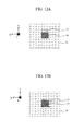
- FIG. 12A is a view showing an example of a cover layer provided only on one side of the core in a Y direction.
- FIG. 12B is a view showing an example of a cover layer provided only on one side of the core in an X direction.
- FIG. 13 is a view showing an example of a spot size converter in which a cover layer is provided on an upper surface and a portion of side surfaces of the core.
- FIG. 14 is a diagram showing a relationship between the thickness of the cover layer in the spot size converter shown in FIG. 13 and the total optical propagation efficiency.
- FIG. 15 is a diagram showing a relationship between the length of the rectangular portion and the total optical propagation efficiency of the spot size converter, for both cases where the cover layer is provided and where not provided.
- FIG. 16 is a view showing an example of a taper shape enlarging two-dimensionally toward an end thereof.
- FIG. 17A is a traverse cross sectional view showing an example of a spot size converter in which an additional rectangular portion (bar-shaped core) is formed on both sides of the taper portion.
- FIG. 17B is a side cross sectional view showing an example of a spot size converter in which an additional rectangular portion (bar-shaped core) is formed on both sides of the taper portion.
- FIG. 18 is a view showing an example of a spot size converter in which a rectangular portion (a bar-shaped core) is formed on both sides of a taper portion and no rectangular portion is formed at an upper part of the taper portion.
- FIG. 19A is a view showing an example of a spot size converter in which a thin core is formed instead of the rectangular portion, as viewed in a direction perpendicular to a light propagation direction.
- FIG. 19B is a view showing an example of a spot size converter in which a thin core is formed instead of the rectangular portion, as viewed in a direction along a light propagation direction.
- FIG. 20 is a diagram showing a relationship between the thickness of the thin core and the total optical propagation efficiency in a spot size converter shown in FIG. 19A and FIG. 19B .
- FIG. 21A is a view showing an example of a spot size converter in which a rectangular portion and a thin core are combined together.
- FIG. 21B is a view showing an example of a spot size converter in which a rectangular portion and a thin core are combined together, and is a view showing an example of a rectangular portion (a bar-shaped core) formed on both sides of a taper portion in addition to the thin core and rectangular portion.
- FIG. 22 is a view showing an example of a spot size converter in which a pair of thin cores is formed in such a manner so as to sandwich a rectangular portion and a taper portion.
- FIG. 23A is a conceptual diagram showing light propagating in two thin cores distanced farther therebetween.
- FIG. 23B is c conceptual diagram showing light propagating in two thin cores distanced closer therebetween.
- FIG. 24A is a conceptual diagram illustrating light coupling from two thin cores to a location above the taper portion in the case the two thin cores are distanced farther therebetween.
- FIG. 24B is a conceptual diagram illustrating light coupling from two thin cores to a location above the taper portion in the case the two thin cores are distanced closer therebetween.
- FIG. 25 is a diagram showing a relationship between the distance between the rectangular portion of a thin core and the taper portion and the total optical propagation efficiency in the spot size converter shown in FIG. 24A and FIG. 24B .
- FIG. 26 is a view showing an example of a spot size converter having a cover layer between a thin core and a clad material.
- FIG. 4 is a perspective view showing an example of a magnetic recording system according to the present invention, with an upper cover removed from a housing 1 .
- FIG. 5 is a cross-sectional view taken along a line A-A of FIG. 4 .
- FIG. 1 is a cross-sectional view of a circumference of a magnetic head comprising a spot size converter, which corresponds to FIG. 5 showing enlarged regions B 1 -B 2 -B 3 -B 4 .
- a magnetic head 5 is fixed to a suspension 6 in such a manner that the position thereof is moved by a voice coil motor 7 .
- a magnetic recording medium 3 rotates by being fixed to a spindle 2 which is driven by a motor in a rotatable mariner.
- ABS Air Bearing Surface
- ABS is formed at a magnetic head bottom surface 16 to generate a negative pressure between the magnetic recording medium 3 and the magnetic head bottom 16 when the magnetic recording medium 3 rotates, so as to float the magnetic head by a floating height of 10 nm or less above the magnetic recording medium 3 .
- the housing 1 includes at least one magnetic recording medium 3 fixed to the spindle 2 and at least one suspension 6 fixed to the voice coil motor 7 .
- a distance S 1 between the suspension 6 and an upper-stage magnetic recording medium 3 is 1 mm or smaller.
- An optical source 4 emitting light necessary for heat assisted magnetic recording and the magnetic head 5 are mounted on each of suspensions 6 .
- the optical source 4 is provided between the suspension 6 and the magnetic head 5 .
- a spot size converter 13 capable of propagating light while reducing the spot size thereof is formed inside the magnetic head.
- Length L 1 of the magnetic head in a Z direction is 230 micrometers.
- a laser diode 10 mounted in a sub-mount 11 and generating light having a wavelength of 760 ⁇ 20 nm or 830 ⁇ 20 nm is used.
- One end surface of the laser diode 10 is machined to have a theta 1 of 40 to 45 degrees in order to reflect light toward the magnetic head bottom surface.
- a light transmission hole 12 is provided on the sub-mount 11 to allow light to enter the spot size converter 13 .
- the light transmission hole 12 is preferably filled with a material which has a low light absorption property and a refractive index higher than air (refractive index >1). With such a configuration, spread of the spot size of light emitted from the laser diode 10 can be suppressed.
- a material for filling the light transmission hole 12 a UV cured resin, a thermosetting adhesive or the like generally used for adhering optical parts is preferable, since such a material suppresses spread of the spot size but also serves to work as an adhesive to adhere the sub-mount 11 and the magnetic head to each other.
- an optical near-field transducer 17 capable of generating a fine light spot may be formed.
- the optical near-field transducer 17 it is preferable to use a metal scatter of a triangular shape as viewed from the magnetic head bottom surface 16 (Optics Letters, Vol. 31, No. 15, Jan. 15, 2006, Page 259).
- a light-shielding film may be formed in a vicinity of the optical near-field transducer 17 to prevent a background light existing in the vicinity of the optical near-filed transducer from being irradiated to the magnetic recording medium 3 .
- the optical near-field transducer 17 may have a V-shaped opening with a portion of the metal scatter connected to a shielding film (Japanese Unexamined Patent Application Publication No. 2001-255254) or have a C-shaped opening (Optics Letters, Vol. 28, No. 15, 2003, page 1320).
- a magnetic field needed for recording is generated by using a thin film coil 18 formed in the magnetic head, and magnetic field thus generated is guided to a terminating end of the spot size converter by a magnetic main pole 19 .
- the magnetic main pole 19 is mounted at a position apart by 200 nm or less from the spot size converter 13 .
- a magnetic return pole 20 for forming a closed magnetic field is formed.
- a magnetic reproducing element 21 for reproducing the recording mark is formed.
- the magnetic reproducing element may be a GMR (Giant Magneto Resistive) element or a TMR (Tunneling Magneto Resistive) element.
- a shield 22 for shielding circumferential magnetic field is formed in the circumference of the magnetic reproducing element 21 .
- magnetic field may be generated after heating the magnetic recording medium 3 by light emitted from the optical source 4 .
- magnetic information may also be recorded in the magnetic recording medium by continuously emitting light to the magnetic recording medium and emitting a magnetic field with desired recording information modulated to a magnetic field pulse.
- magnetic information may be recorded in the magnetic recording medium by continuously generating magnetic field and emitting light pulse-modulated with desired recording information.
- a magnetic reproducing element 21 formed in the magnetic head shown in FIG. 1 is used.
- the reproduction signal is processed by signal processing LSI 8 shown in FIG. 3 .
- the spot size converter formed inside the magnetic head is described in detail.
- the spot size converter 13 is covered with a clad material 24 .
- the spot size converter 13 serves to directly couple with light (incident light 9 ) emitted from the optical source 4 and propagate the light up to the magnetic head bottom surface 16 and irradiate light of a fine sport size onto the magnetic recording medium. Therefore, the spot size converter 13 extends from an upper surface of the magnetic head toward the magnetic head bottom surface 16 .
- FIG. 6A is a cross-sectional view along a line C-C of FIG. 1
- FIG. 6B is a cross-sectional view along a line D-D of FIG. 1
- the spot size converter 13 has layers 15 which are formed between top and bottom of the core 14 in a Y direction and the clad material 24 in such a manner so as to contact the core.
- a cover layer 15 such a layer contacting the core is referred to as a cover layer 15 .
- the cover layer 15 is characterized by having a lower refractive index than those of the core 14 and the clad material 24 .
- Thickness of cover layers 15 formed at top and bottom of the core 14 in the Y direction is t 2 /2 respectively, with a total thickness of t 2 .
- a refractive index of the core 14 is higher than that of the clad material 24 .
- a shape of the spot size converter viewed in the XZ plane is a shape composed of a substantially rectangular shape and a taper shape (trapezoidal) following the rectangular shape and having a width enlarging toward a magnetic head bottom surface.
- the shape of the cover layer 15 viewed in the XZ plane is also a shape substantially equivalent to a shape of the core 14 .
- a length L 2 +L 3 of the spot size converter in a Z direction is 230 micrometers, a length (L 1 ) of the magnetic head.
- the rectangular portion of the spot size converter 13 serves to couple with incident light 9 and flatten wavefront of the propagating light, and the taper portion serves to reduce the spot size of the light.
- the clad material 24 , the core 14 and the cover layer 15 are respectively made of Al 2 O 3 having a refractive index of 1.57 to 1.66, Ta 2 O 5 having a refractive index of 2.13, and SiO 2 having a refractive index of 1.45.
- the optical waveguide spot size converter is a kind of the optical waveguide
- Si 3 N 4 refractive index difference delta-n between the core and the clad material is same. Therefore, for example, Si 3 N 4 (refractive index: 1.89 to 2.10) may be used for the core 14
- SiO 2 —Si 3 N 4 may be used for the clad material 24 .
- the refractive index of SiO 2 —Si 3 N 4 , a material of the clad material 24 may be adjusted within a range between 1.45 and 2.10 by simultaneously spattering SiO 2 and Si 3 N 4 by a spattering method while controlling a film forming rate of SiO 2 and Si 3 N 4 .
- a core terminating end width w 2 of the spot size converter 13 is 0.5 or 0.6 micrometers, and a core terminating end thickness t 1 is 0.2 or 0.3 micrometers.
- the spot size converter 13 serves to irradiate light of a fine sport size to the magnetic recording medium.
- a width and a thickness of a high refractive index core at the magnetic head bottom surface need to be same as the size of the optical near-field transducer (both width and thickness: 0.6 micrometers or smaller). Therefore, both the width w 2 and the thickness t 1 are preferably 0.6 micrometers or smaller.
- the core of the spot size converter may be shaped in such a manner that a lower portion of the core terminating end of the taper portion is further extended.
- FIG. 7A is a cross-sectional view of the spot size converter in a direction perpendicular to a light propagation direction
- FIG. 7B is a cross-sectional view in a direction along the light propagation direction.
- a length L 2 +L 3 +L 4 of the spot size converter in a Z direction is a length (L 1 ) of the magnetic head.
- a magnetic main pole 19 In a vicinity of the core terminating end of the magnetic head, there exist a magnetic main pole 19 , a magnetic return pole 20 and a thin film coil 18 .
- either or both of the core tip end w 1 and the thickness t 1 at the tip end of the spot size converter 13 is reduced to be not larger than a width or a thickness that induces the seeping mode described above, and the core is sandwiched between cover layers 15 .
- a refractive index difference delta-n between the core and the clad can be effectively reduced, whereby the spot size of light which can be coupled to and propagated in the tip end can be enlarged, and as a result, incident light 9 having a large spot size shown in FIG. 1 can be efficiently coupled to the spot size converter 13 .
- a width or a thickness (Ww) to an extent that induces the seeping mode can be expressed approximately with a formula shown below by modifying a standing wave conditional equation for a zero order mode in the optical waveguide.
- ⁇ 1 is represents a critical angle of the light at an interface between the core and the clad and can be expressed with a formula shown below.
- ⁇ 1 sin - 1 ( n 1 2 - n 2 2 n 1 ) ( 2 ) Where;
- n 1 refractive index of core material
- n 2 refractive index of clad material
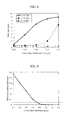
- FIG. 8 a calculation result of the spot size of light which can be coupled to and propagated in the core tip end of the spot size converter 13 obtained by using the Beam Propagation Method (BPM) is shown in FIG. 8 .
- the horizontal axis in FIG. 8 represents a thickness t 2 /2 of the cover layer, and the vertical axis represents the spot size of light which can be coupled to and propagated in the core tip end.
- a width (Ww) to the extent that induces the seeping mode according to the present embodiment is about 290 nm.
- the core 14 provided with the cover layer can increase the spot size of light which can be coupled and propagated.
- either or both of the core width w 1 and the core thickness t 1 is defined as 290 nm
- either or both of the core width w 1 and the core thickness t 1 is defined as 310 nm or less from the above formula for calculating Ww.
- the thickness t 2 of the cover layer 15 shown in FIG. 6A may be adjusted approximately to a value (Tc) expressed in a formula shown below.
- n 1 refractive index of core material
- n 2 refractive index of clad material
- n 3 refractive index of cover layer
- Ww approximate width or thickness that induces the seeping mode expressed in Formula (1)
- t 2 becomes a thickness of Tc
- a refractive index difference delta-n between the core and the clad can be zero effectively, whereby the spot size of light which can be coupled to and propagated in a tip end of the spot size converter 13 can be made maximum, and as a result, incident light 9 having a large spot size shown in FIG. 1 can be coupled to the spot size converter efficiently.
- FIG. 9 is a diagram showing a relationship of the effective refractive index difference between the core and the clad with respect to the thickness of the cover layer.
- the horizontal axis in FIG. 9 shows the thickness t 2 of the cover layer, and the vertical axis shows the efficient refractive index difference between the core and the clad.
- a thickness of the cover layer making the efficient refractive index difference zero is defined as 1.0, which represents a calculation result obtained when either or both of the core width w 1 and the core thickness t 1 is smaller than the above Ww.
- FIG. 9 shows that the efficient refractive index is 0.05 or lower when Tc is approximately 70% of a thickness of the cover layer making the refractive index difference zero.
- FIG. 10 a calculation result of the dependency of the total optical propagation efficiency of the spot size converter 13 on the thickness t 2 of the cover layer obtained by using the BPM method is shown in FIG. 10 .
- the horizontal axis in FIG. 10 shows the thickness t 2 /2 of the cover layer, and the vertical axis shows the total optical propagation efficiency (power of light emitted from spot size converter/power of incident light) of the spot size converter.
- the total optical propagation efficiency can be made maximum when the thickness t 2 of the cover layer is a thickness within a range of approximately ⁇ 30% of Tc expressed in the above formula. Therefore, it is preferable that the thickness t 2 of the cover layer is within a range of ⁇ 30% of Tc expressed in the above formula.
- the thickness t 2 /2 of the cover layer can be determined by newly obtaining Tc of 830 ⁇ 20 nm by assigning 830 ⁇ 20 nm to the wavelength lambda in the above formula for calculating Ww.
- an optimum value may also be determined by making a cross-sectional area thereof equal to the cross-sectional area of the cover layer determined in a configuration shown in FIG. 6A and FIG. 6B as described above.
- a thickness or a width of cover layers shown in FIG. 6A , FIG. 6B , FIG. 7A , FIG. 7B , FIG. 11A and FIG. 11B may be different between an upper layer and a lower layer and between a left layer and a right layer respectively.
- cover layers having a thickness same as a thickness of the upper core layer may be formed on an upper layer of the core 14 and on a portion of side surfaces of the core 14 .
- a total length of cover layers on side surfaces of the core is 10 times the width w 1 of the core 14 .
- FIG. 14 A calculation result of the dependency of the total optical propagation efficiency on the thickness t 2 of the cover layer by using the BPM method is shown in FIG. 14 .
- the horizontal axis of FIG. 14 shows the thickness t 2 /2 of the cover layer, and the vertical axis shows the total optical propagation efficiency of the spot size converter.
- an equivalent total optical propagation efficiency can be achieved with an approximately 1 ⁇ 4 thickness t 2 of the cover layer when compared with a configuration example shown in FIG. 6A and FIG. 6B . Therefore, in a configuration example shown in FIG. 13 , it is preferable that a thickness of the cover layer is approximately 1 ⁇ 4 of an optimum thickness of the cover layer obtained for a configuration example shown in FIG. 6A and FIG. 6B .
- a substantially rectangular shape (hereinafter, referred to as a rectangular portion) as viewed in the XZ plane is formed on top of the taper portion as shown in FIG. 6B .
- Light coupling to and propagating in such a rectangular portion has a wavefront thereof flattened before the light reaches the taper portion, whereby a loss caused when the spot size is reduced in the taper portion can be suppressed.
- FIG. 15 a calculation result of the dependency of the total optical propagation efficiency of the spot size converter 13 on the length L 2 of the rectangular portion obtained by using the BPM method is shown in FIG. 15 .
- the horizontal axis of FIG. 15 shows the length L 2 of the rectangular portion, and the vertical axis shows the total optical propagation efficiency of the spot size converter.
- L 2 of the rectangular portion is defined as 90 micrometers.
- the shape of the above taper portion may be a shape having a width becoming larger toward the terminating end of the spot size converter as shown in FIG. 16 . Further, a similar effect can be obtained even when the taper portion has a taper shape in which the core thickness becomes thinner toward the light incident side similarly with a spot size converter shown in FIG. 6B and FIG. 16 (in this case, the core thickness is a thickness in a Y axis direction).
- calculations are made with both 760 ⁇ 20 nm and 830 ⁇ 20 nm as a wavelength of the incident light and linear polarized light in the Y direction as the polarization.
- the thickness t 1 of the spot size converter is 0.2 micrometers
- FIG. 17A is a cross-sectional view of a spot size converter in a direction vertical to a light propagation direction
- FIG. 17B is a cross-sectional view in a direction along the light propagation direction.
- a distance s 1 between a rectangular portion at the center and a bar-shaped core on each side thereof is preferably not larger than a radius of the spot of light propagating in the rectangular portion (bar-shaped core).
- the cross sectional shape of the bar-shaped core on both sides needs not to be identical with a shape of the rectangular portion on top of the taper portion.
- a thickness t 3 of a cover layer in the bar-shaped core on both sides is preferably not smaller than a thickness t 2 of a cover layer in the rectangular portion on top of the taper portion.
- a thickness t 3 of a cover layer in the bar-shaped core on both sides is preferably not larger than a thickness t 2 of a cover layer in the rectangular portion on top of the taper portion.
- total optical propagation efficiency equal to or higher than in a configuration example shown in FIG. 6B can be achieved even when the spot size converter has a configuration without a rectangular portion on top of the taper portion as shown in FIG. 18 .
- a portion serving to couple the incident light 9 and flatten the wavefront of the propagating light includes a core and a clad only, but no a rectangular portion in which a cover layer 15 made of a material having a refractive index lower than those of a core 14 and a clad material 24 is formed at upper and lower sides (top and bottom as viewed in Y direction) of the core like Embodiment 1.
- FIG. 19A is a cross sectional view of a spot size converter according to the present invention in a direction perpendicular to a light propagation direction
- FIG. 19B is a cross sectional view of the spot size converter in a direction along the light propagation direction.
- a thin core 25 may be formed on a side of the light emitting core instead of forming a rectangular portion on top or sides of the taper portion.
- An optical waveguide comprising a core and a clad and having effects of coupling with the incident light 9 and flattening wavefront of the propagating light is preferably to have a core width or thickness equivalent to or less than a width or a thickness (Ww) to an extent that induces the seeping mode.
- a thin core 25 having a width w 4 of 5 micrometers and a thickness t 4 of 0.2 micrometers and made of a core material of Al 2 O 3 —Si 3 N 4 .
- a calculation result of the dependency of the total optical propagation efficiency of the spot size converter 13 on the length L 4 of the thin core 25 by the BPM method is shown in FIG. 20 .
- the horizontal axis of FIG. 20 shows a length L 4 of the thin core 25
- the vertical axis shows the total optical propagation efficiency of the spot size converter.
- a distance d 1 between the thin core 25 and a taper portion is defined as 0 to 0.3 micrometers, and an light incident in the spot size converter is emitted in such a manner that the wavefront of light becomes spherical at a tip end of the spot size converter by freely propagating of alight having the spot light of about 3 micrometers in air (in a medium having a refractive index of 1) in distance of 30 micrometers only.
- the polarization is a linear polarized light in the Y direction.
- a length L 4 +L 3 of the spot size converter 13 in a Z direction is 230 micrometers, a length (L 1 ) of the magnetic head.
- the total optical propagation efficiency becomes maximum when the length L 4 of the thin type film is approximately 90 micrometers, about 1.6 times compared when the length L 4 of the thin core is 0.0 micrometer.
- the efficiency when L 4 is longer than 90 micrometers is dropped by a spot size conversion loss resulting from shortening of a length L 2 of the taper portion serving to reduce the spot size. Accordingly, when there is no limit to the length of the magnetic head, L 4 is preferably set to 90 micrometers or longer.
- the length L 4 of the thin core is defined as 90 micrometers.
- the length of the thin core 25 needs to extent at least from a surface opposite to ABS of the magnetic field to an inlet portion of the core 14 , and preferably extents up to ABS of the magnetic head at maximum. Because, if a length of the thin core 25 does not reach an inlet of the core 14 , light propagating in the thin core 25 may be enlarged in the clad material 24 and coupled to the core 14 before coupling therewith, whereby a large light coupling loss occurs and as a result, the total optical propagation efficiency of the spot size converter drops.
- a thin core 25 is formed instead of a rectangular portion. But, a rectangular portion and a thin core 25 may be formed together as shown in FIG. 21 . Further, as shown in FIG. 21B , a rectangular portion and an additional rectangular portion (bar-shaped core) may be formed on sides of the rectangular portion, and a thin core 25 may be formed.
- a rectangular portion and an additional rectangular portion may be formed on sides of the rectangular portion, and a thin core 25 may be formed.
- a single thin core 25 is formed. But, as shown in FIG. 22 , But, it may be a configuration in which a pair of thin cores 25 sandwiches either or both (hereinafter, referred to as a main core portion) of a rectangular portion and a taper portion in which a cover layer 15 made of a material having a refractive index lower than those of the core 14 and the clad material 24 is formed on top and bottom of the core 14 in the Y direction.
- a cover layer 15 made of a material having a refractive index lower than those of the core 14 and the clad material 24 is formed on top and bottom of the core 14 in the Y direction.
- FIG. 23A and FIG. 23B are cross sectional views of two thin cores viewed from Y and Z surfaces, and schematic views illustrating the intensity profile (light spot) of light propagating in two thin film type cores of a same shape
- the light spot 27 shown in the figures propagates along each of the thin cores 25 .
- an interval d 1 +d 2 between the cores is small as shown in FIG. 23B , light spots 27 overlap each other having a substantially same intensity distribution as one light spot, whereby the coupling efficiency of two thin cores 25 and incident light becomes almost same as an efficiency of one thin core.
- the coupling efficiency becomes equivalent to light propagating in each of the two thin cores.
- the coupling efficiency can be made about twice when compared with a small interval d 1 +d 2 .
- FIG. 24A and FIG. 24B are cross sectional views of the spot size converter as viewed in the YZ plane, schematically showing the intensity profile (light spot 28 ) of light propagating in the thin core 25 and light propagating in an upper part of the main core.
- FIG. 25 is a calculation result thereof.
- the total optical propagation efficiency shown by the vertical axis is standardized with a utilization efficiency of one thin core as 1. With an interval d 1 +d 2 of about 1.2 to 1.8 micrometers, the total optical propagation efficiency could be enhanced to 1.3 times or more of that in the case of using a single thin core. In this case, a half width of the spot size in the Y direction of light propagating along a thin core is approximately 1.1 to 2.2 micrometers.
- the interval d 1 +d 2 is defined as 1.5 micrometers or 1.7 micrometers. If width, thickness and delta-n of the thin core are given, a half width of the spot size in the Y direction of light propagating in the vicinity of the thin core can be derived by using the BPM method.
- two thin cores 25 are substantially identical, width, thickness and delta-n of respective thin cores may be different, provided that d 1 and d 2 are not larger than a half value of the half width of the spot size in the Y direction of light propagating along each of the thin cores ⁇ 20%.
- a thin core in which a cover layer 15 made of a material having a refractive index lower than those of the core 25 and the clad material 24 is formed between top and bottom of the core in the Y direction and between the core 25 and the clad material 24 as shown in FIG. 26 may be used.
- the thin core can couple with incident light 9 having a larger spot size, whereby the total optical propagation efficiency of the spot size converter can be enhanced.
Abstract
Description
- Patent Document 1: JP 2007-257753 A
- Patent Document 2: JP 08-330673 A
- Non-Patent Document 1: Japanese Journal of Applied Physics, Vol. 45, No. 2B, 2006, p.p. 1314-1320
- Non-Patent Document 2: Optics Letters, Vol. 28, No. 15, 2003, p.p. 1302-1304
Where;
Where;
n 1 ·t 1 +n 3 ·A=n 2·(t 1 +A) (4)
- 1 Housing
- 2 Spindle
- 3 Magnetic recording medium
- 4 Optical source
- 5 Magnetic head
- 6 Suspension
- 7 Voice coil motor
- 8 Signal processing LSI
- 9 Incident light
- 10 Laser diode
- 11 Sub-mount
- 12 Light transmission hole
- 13 Spot size converter
- 14 Core
- 15 Cover layer
- 16 Magnetic head bottom
- 17 Optical near-field transducer
- 18 Thin film coil
- 19 Magnetic main pole
- 20 Magnetic return pole
- 21 Magnetic reproducing element
- 22 Shield
- 23 Magnetic head base metal
- 24 Clad material
- 25 Thin core
- 26 Light intensity profile
- 27 light spot propagating in thin core
- 28 light spot propagating in main core
Claims (9)
n 1 ·t 1 +n 3 ·A=n 2·(t 1 +A)
n 1 ·t 1 +n 3 ·A=n 2·(t 1 +A)
Applications Claiming Priority (3)
| Application Number | Priority Date | Filing Date | Title |
|---|---|---|---|
| JP2010-144662 | 2010-06-25 | ||
| JP2010144662A JP5020354B2 (en) | 2010-06-25 | 2010-06-25 | Thermally assisted recording magnetic head and magnetic recording apparatus equipped with the same |
| PCT/JP2011/061137 WO2011162042A1 (en) | 2010-06-25 | 2011-05-16 | Heat-assisted recording-use magnetic head and magnetic recording device equipped with same |
Publications (2)
| Publication Number | Publication Date |
|---|---|
| US20120182842A1 US20120182842A1 (en) | 2012-07-19 |
| US8780678B2 true US8780678B2 (en) | 2014-07-15 |
Family
ID=45371243
Family Applications (1)
| Application Number | Title | Priority Date | Filing Date |
|---|---|---|---|
| US13/392,115 Expired - Fee Related US8780678B2 (en) | 2010-06-25 | 2011-05-16 | Thermal-assisted-magnetic-recording head having core cover layer |
Country Status (3)
| Country | Link |
|---|---|
| US (1) | US8780678B2 (en) |
| JP (1) | JP5020354B2 (en) |
| WO (1) | WO2011162042A1 (en) |
Cited By (4)
| Publication number | Priority date | Publication date | Assignee | Title |
|---|---|---|---|---|
| US20150043877A1 (en) * | 2012-04-24 | 2015-02-12 | Seagate Technology Llc | Optical devices including assistant layers |
| US20180025747A1 (en) * | 2016-07-21 | 2018-01-25 | Western Digital (Fremont), Llc | Heat assisted magnetic recording write apparatus having an inverse tapered waveguide |
| US10106889B2 (en) | 2014-11-11 | 2018-10-23 | Seagate Technology Llc | Waveguides including novel core materials |
| US10127937B1 (en) * | 2016-02-29 | 2018-11-13 | Seagate Technology Llc | Optically opaque overlay for a waveguide of a heat-assisted magnetic recording slider |
Families Citing this family (11)
| Publication number | Priority date | Publication date | Assignee | Title |
|---|---|---|---|---|
| JP4881989B2 (en) * | 2009-10-15 | 2012-02-22 | 株式会社日立製作所 | Magnetic head for thermally assisted recording and magnetic recording apparatus using the same |
| US8588039B1 (en) * | 2011-03-02 | 2013-11-19 | Western Digital (Fremont), Llc | Energy-assisted magnetic recording head having multiple cores of different lengths |
| JP5145443B2 (en) | 2011-06-23 | 2013-02-20 | 株式会社日立製作所 | Magnetic head for thermal assist recording and magnetic recording apparatus |
| US9093086B2 (en) * | 2013-12-06 | 2015-07-28 | HGST Netherlands B.V. | Thermally-assisted magnetic recording head |
| US9396749B2 (en) * | 2014-04-21 | 2016-07-19 | Seagate Technology Llc | Waveguide core layer with reduced downtrack thickness proximate a near-field transducer |
| US9053716B1 (en) * | 2014-05-07 | 2015-06-09 | HGST Netherlands B.V. | Spot size converter with a plurality of branches for HAMR heads |
| US9129634B1 (en) * | 2014-06-17 | 2015-09-08 | HGST Netherlands B.V. | Integrated compound DBR laser for HAMR applications |
| US9280994B1 (en) * | 2014-09-22 | 2016-03-08 | HGST Netherlands B.V. | Thermally assisted magnetic recording head with optical spot-size converter attached two dimensional thin waveguide |
| US9524740B2 (en) * | 2014-10-23 | 2016-12-20 | Seagate Technology Llc | Waveguide of a write head with reduced crosstrack width proximate a near-field transducer |
| US9558764B2 (en) * | 2014-10-23 | 2017-01-31 | Seagate Technology Llc | Waveguide of a write head with reduced cross sectional area proximate a near-field transducer |
| CN111145788A (en) * | 2018-11-02 | 2020-05-12 | 新科实业有限公司 | Thermally assisted magnetic recording head and thermally assisted magnetic recording disk drive |
Citations (17)
| Publication number | Priority date | Publication date | Assignee | Title |
|---|---|---|---|---|
| JPH08330673A (en) | 1995-06-02 | 1996-12-13 | Fujitsu Ltd | Optical semiconductor device |
| US6950598B1 (en) | 2004-09-02 | 2005-09-27 | Fujitsu Limited | Light emitting head, information storage device, and composite head manufacturing method |
| JP2007257753A (en) | 2006-03-24 | 2007-10-04 | Konica Minolta Opto Inc | Micro optical recording head and its manufacturing method |
| US7359599B2 (en) | 2006-04-12 | 2008-04-15 | Hitachi, Ltd. | Optical near-field generator and near-field optical recording and reproduction apparatus |
| US20090052077A1 (en) * | 2007-08-23 | 2009-02-26 | Tdk Corporation | Thermally assisted magnetic head with optical waveguide and light shield |
| US20090185459A1 (en) | 2008-01-18 | 2009-07-23 | Takuya Matsumoto | Head gimbal assembly and information recording apparatus |
| JP2009176354A (en) | 2008-01-23 | 2009-08-06 | Konica Minolta Opto Inc | Optical element, slider and optical head |
| WO2010016262A1 (en) | 2008-08-08 | 2010-02-11 | 株式会社日立製作所 | Thermally assisted magnetic head and method for assembling thermally assisted magnetic head |
| US20110090770A1 (en) * | 2009-10-15 | 2011-04-21 | Hitachi, Ltd. | Thermal-assisted-magnetic-recording head and magnetic recording system using the thermal-assisted-magnetic-recoring head |
| US20110205660A1 (en) * | 2010-02-25 | 2011-08-25 | Tdk Corporation | Spot size converter and thermal assist magnetic recording head therewith |
| US20110216635A1 (en) | 2010-03-05 | 2011-09-08 | Hitachi, Ltd. | Head for thermal assisted magnetic recording device, and thermal assisted magnetic recording device |
| US20110235478A1 (en) * | 2010-03-23 | 2011-09-29 | Tdk Corporation | Wave guide that attenuates evanescent light of higher order tm mode |
| US20110310713A1 (en) * | 2010-06-22 | 2011-12-22 | Tdk Corporation | Thermally assisted head having reflection mirror for propagating light |
| US8098547B2 (en) * | 2010-03-09 | 2012-01-17 | Tdk Corporation | Optical waveguide and thermal assist magnetic recording head therewith |
| US20120147716A1 (en) * | 2010-12-08 | 2012-06-14 | Tdk Corporation | Thermally-assisted magnetic head |
| US20120147717A1 (en) * | 2010-12-09 | 2012-06-14 | Rohm Co., Ltd. | Method of burn-in testing for thermally assisted head |
| US20120327751A1 (en) * | 2011-06-23 | 2012-12-27 | Hitachi, Ltd. | Magnetic recording system used thermal-assisted-magnetic- recording head |
-
2010
- 2010-06-25 JP JP2010144662A patent/JP5020354B2/en active Active
-
2011
- 2011-05-16 US US13/392,115 patent/US8780678B2/en not_active Expired - Fee Related
- 2011-05-16 WO PCT/JP2011/061137 patent/WO2011162042A1/en active Application Filing
Patent Citations (20)
| Publication number | Priority date | Publication date | Assignee | Title |
|---|---|---|---|---|
| JPH08330673A (en) | 1995-06-02 | 1996-12-13 | Fujitsu Ltd | Optical semiconductor device |
| US5787106A (en) | 1995-06-02 | 1998-07-28 | Fujitsu Limited | Optical semiconductor device for changing a beam diameter |
| US6950598B1 (en) | 2004-09-02 | 2005-09-27 | Fujitsu Limited | Light emitting head, information storage device, and composite head manufacturing method |
| JP2006073105A (en) | 2004-09-02 | 2006-03-16 | Fujitsu Ltd | Optical irradiation head, information storage device, and combined head manufacturing method |
| JP2007257753A (en) | 2006-03-24 | 2007-10-04 | Konica Minolta Opto Inc | Micro optical recording head and its manufacturing method |
| US7359599B2 (en) | 2006-04-12 | 2008-04-15 | Hitachi, Ltd. | Optical near-field generator and near-field optical recording and reproduction apparatus |
| US20090052077A1 (en) * | 2007-08-23 | 2009-02-26 | Tdk Corporation | Thermally assisted magnetic head with optical waveguide and light shield |
| US20090185459A1 (en) | 2008-01-18 | 2009-07-23 | Takuya Matsumoto | Head gimbal assembly and information recording apparatus |
| JP2009170053A (en) | 2008-01-18 | 2009-07-30 | Hitachi Ltd | Head gimbal assembly and information recording device |
| JP2009176354A (en) | 2008-01-23 | 2009-08-06 | Konica Minolta Opto Inc | Optical element, slider and optical head |
| WO2010016262A1 (en) | 2008-08-08 | 2010-02-11 | 株式会社日立製作所 | Thermally assisted magnetic head and method for assembling thermally assisted magnetic head |
| US20110090770A1 (en) * | 2009-10-15 | 2011-04-21 | Hitachi, Ltd. | Thermal-assisted-magnetic-recording head and magnetic recording system using the thermal-assisted-magnetic-recoring head |
| US20110205660A1 (en) * | 2010-02-25 | 2011-08-25 | Tdk Corporation | Spot size converter and thermal assist magnetic recording head therewith |
| US20110216635A1 (en) | 2010-03-05 | 2011-09-08 | Hitachi, Ltd. | Head for thermal assisted magnetic recording device, and thermal assisted magnetic recording device |
| US8098547B2 (en) * | 2010-03-09 | 2012-01-17 | Tdk Corporation | Optical waveguide and thermal assist magnetic recording head therewith |
| US20110235478A1 (en) * | 2010-03-23 | 2011-09-29 | Tdk Corporation | Wave guide that attenuates evanescent light of higher order tm mode |
| US20110310713A1 (en) * | 2010-06-22 | 2011-12-22 | Tdk Corporation | Thermally assisted head having reflection mirror for propagating light |
| US20120147716A1 (en) * | 2010-12-08 | 2012-06-14 | Tdk Corporation | Thermally-assisted magnetic head |
| US20120147717A1 (en) * | 2010-12-09 | 2012-06-14 | Rohm Co., Ltd. | Method of burn-in testing for thermally assisted head |
| US20120327751A1 (en) * | 2011-06-23 | 2012-12-27 | Hitachi, Ltd. | Magnetic recording system used thermal-assisted-magnetic- recording head |
Non-Patent Citations (2)
| Title |
|---|
| Tim Rausch et al., Near Field Heat Assisted Magnetic Recording with a Planar Solid Immersion Lens, Japanese Journal of Applied Physics, 2006, pp. 1314-1320, vol. 45, No. 2B. |
| Vilson R. Almeida et al., Naotaper for compact mode conversion, Optics Letters, Aug. 1, 2003, pp. 1302-1304, vol. 28, No. 15. |
Cited By (6)
| Publication number | Priority date | Publication date | Assignee | Title |
|---|---|---|---|---|
| US20150043877A1 (en) * | 2012-04-24 | 2015-02-12 | Seagate Technology Llc | Optical devices including assistant layers |
| US9316783B2 (en) * | 2012-04-24 | 2016-04-19 | Seagate Technology Llc | Optical devices including assistant layers |
| US10106889B2 (en) | 2014-11-11 | 2018-10-23 | Seagate Technology Llc | Waveguides including novel core materials |
| US10127937B1 (en) * | 2016-02-29 | 2018-11-13 | Seagate Technology Llc | Optically opaque overlay for a waveguide of a heat-assisted magnetic recording slider |
| US20180025747A1 (en) * | 2016-07-21 | 2018-01-25 | Western Digital (Fremont), Llc | Heat assisted magnetic recording write apparatus having an inverse tapered waveguide |
| US9978410B2 (en) * | 2016-07-21 | 2018-05-22 | Western Digital (Fremont), Llc | Heat assisted magnetic recording write apparatus having an inverse tapered waveguide |
Also Published As
| Publication number | Publication date |
|---|---|
| WO2011162042A1 (en) | 2011-12-29 |
| JP2012009113A (en) | 2012-01-12 |
| US20120182842A1 (en) | 2012-07-19 |
| JP5020354B2 (en) | 2012-09-05 |
Similar Documents
| Publication | Publication Date | Title |
|---|---|---|
| US8780678B2 (en) | Thermal-assisted-magnetic-recording head having core cover layer | |
| US8400887B2 (en) | Magnetic recording system used thermal-assisted-magnetic-recording head | |
| JP4881989B2 (en) | Magnetic head for thermally assisted recording and magnetic recording apparatus using the same | |
| JP4800889B2 (en) | Heat-assisted magnetic recording head and method for manufacturing the same | |
| US7652775B2 (en) | Optical near-field generator and recording and reproduction apparatus | |
| US8194509B2 (en) | Thermally-assisted magnetic recording head comprising light source with photonic-band layer | |
| US8200054B1 (en) | High efficiency grating coupling for light delivery in EAMR | |
| JP4642738B2 (en) | Heat-assisted magnetic recording head | |
| US8270259B2 (en) | Near-field optical head including waveguide having polyhedron core | |
| JP5008101B2 (en) | Thermally assisted magnetic recording head with converging lens | |
| US20120072931A1 (en) | Surface emitting semiconductor laser, optical recording head, and optical recording apparatus | |
| KR101442086B1 (en) | Recording head with near-field antenna and composite pole | |
| JP2011090752A (en) | Thermal-assisted recording head, thermal-assisted recording device, and near-field light generating apparatus | |
| US9424867B2 (en) | Excitation of a near-field transducer using combined transverse electric and transverse magnetic modes | |
| US8547804B2 (en) | Thermally-assisted recording head and magnetic recording system | |
| US20100046111A1 (en) | Recording head and data recording and reproducing apparatus | |
| JP2009087499A (en) | Thermal assist magnetic recording element, and magnetic head and magnetic recording device using the same | |
| US8619511B1 (en) | Heat-assisted magnetic recording head with optical spot-size converter fabricated in 2-dimensional waveguide | |
| US9280994B1 (en) | Thermally assisted magnetic recording head with optical spot-size converter attached two dimensional thin waveguide | |
| JP5666994B2 (en) | Thermally assisted magnetic recording head and magnetic disk apparatus | |
| JP2012033211A (en) | Heat-assisted integrated head and heat-assisted recording apparatus | |
| US8537645B1 (en) | Near field light generating element, thermally assisted magnetic head, thermally assisted magnetic head device and thermally assisted magnetic recording/reproducing apparatus | |
| JP4312727B2 (en) | Composite head and magnetic recording / reproducing apparatus including the same |
Legal Events
| Date | Code | Title | Description |
|---|---|---|---|
| AS | Assignment |
Owner name: HITACHI, LTD., JAPAN Free format text: ASSIGNMENT OF ASSIGNORS INTEREST;ASSIGNORS:IWANABE, YASUHIKO;MATSUMOTO, TAKUYA;MIYAMOTO, HARUKAZU;SIGNING DATES FROM 20120216 TO 20120306;REEL/FRAME:027892/0709 |
|
| STCF | Information on status: patent grant |
Free format text: PATENTED CASE |
|
| MAFP | Maintenance fee payment |
Free format text: PAYMENT OF MAINTENANCE FEE, 4TH YEAR, LARGE ENTITY (ORIGINAL EVENT CODE: M1551) Year of fee payment: 4 |
|
| FEPP | Fee payment procedure |
Free format text: MAINTENANCE FEE REMINDER MAILED (ORIGINAL EVENT CODE: REM.); ENTITY STATUS OF PATENT OWNER: LARGE ENTITY |
|
| LAPS | Lapse for failure to pay maintenance fees |
Free format text: PATENT EXPIRED FOR FAILURE TO PAY MAINTENANCE FEES (ORIGINAL EVENT CODE: EXP.); ENTITY STATUS OF PATENT OWNER: LARGE ENTITY |
|
| STCH | Information on status: patent discontinuation |
Free format text: PATENT EXPIRED DUE TO NONPAYMENT OF MAINTENANCE FEES UNDER 37 CFR 1.362 |
|
| FP | Lapsed due to failure to pay maintenance fee |
Effective date: 20220715 |