US8764197B2 - Polarization conversion element, polarization converting unit, and projecting apparatus - Google Patents
Polarization conversion element, polarization converting unit, and projecting apparatus Download PDFInfo
- Publication number
- US8764197B2 US8764197B2 US13/439,136 US201213439136A US8764197B2 US 8764197 B2 US8764197 B2 US 8764197B2 US 201213439136 A US201213439136 A US 201213439136A US 8764197 B2 US8764197 B2 US 8764197B2
- Authority
- US
- United States
- Prior art keywords
- polarization conversion
- light
- phase difference
- optical
- polarized light
- Prior art date
- Legal status (The legal status is an assumption and is not a legal conclusion. Google has not performed a legal analysis and makes no representation as to the accuracy of the status listed.)
- Active, expires
Links
Images


Classifications
-
- G—PHYSICS
- G02—OPTICS
- G02B—OPTICAL ELEMENTS, SYSTEMS OR APPARATUS
- G02B27/00—Optical systems or apparatus not provided for by any of the groups G02B1/00 - G02B26/00, G02B30/00
- G02B27/28—Optical systems or apparatus not provided for by any of the groups G02B1/00 - G02B26/00, G02B30/00 for polarising
- G02B27/286—Optical systems or apparatus not provided for by any of the groups G02B1/00 - G02B26/00, G02B30/00 for polarising for controlling or changing the state of polarisation, e.g. transforming one polarisation state into another
-
- G—PHYSICS
- G02—OPTICS
- G02B—OPTICAL ELEMENTS, SYSTEMS OR APPARATUS
- G02B27/00—Optical systems or apparatus not provided for by any of the groups G02B1/00 - G02B26/00, G02B30/00
- G02B27/28—Optical systems or apparatus not provided for by any of the groups G02B1/00 - G02B26/00, G02B30/00 for polarising
- G02B27/283—Optical systems or apparatus not provided for by any of the groups G02B1/00 - G02B26/00, G02B30/00 for polarising used for beam splitting or combining
- G02B27/285—Optical systems or apparatus not provided for by any of the groups G02B1/00 - G02B26/00, G02B30/00 for polarising used for beam splitting or combining comprising arrays of elements, e.g. microprisms
-
- G—PHYSICS
- G03—PHOTOGRAPHY; CINEMATOGRAPHY; ANALOGOUS TECHNIQUES USING WAVES OTHER THAN OPTICAL WAVES; ELECTROGRAPHY; HOLOGRAPHY
- G03B—APPARATUS OR ARRANGEMENTS FOR TAKING PHOTOGRAPHS OR FOR PROJECTING OR VIEWING THEM; APPARATUS OR ARRANGEMENTS EMPLOYING ANALOGOUS TECHNIQUES USING WAVES OTHER THAN OPTICAL WAVES; ACCESSORIES THEREFOR
- G03B21/00—Projectors or projection-type viewers; Accessories therefor
- G03B21/14—Details
- G03B21/20—Lamp housings
- G03B21/2073—Polarisers in the lamp house
Definitions
- the present invention relates to a polarization conversion element that is used for converting randomly-polarized light beams emitted from a light source into one type of a polarized light beam.
- Projection-type video systems such as liquid crystal projectors are devices that modulate light emitted from a light source device in accordance with image information and project a modulated optical image onto a screen in an enlarged scale.
- polarization conversion elements are used for splitting light (hereinafter, referred to as random light) including randomly-polarized light beams (polarized light beams such as a P-polarized light beam and an S-polarized light beam of which the polarization planes are perpendicular to each other, light beams in which linearly polarized light beams of which the directions of polarization planes are various are mixed, circularly-polarized light beams, and elliptically-polarized light beams) emitted from a light source device into a plurality of intermediate light beams, converting the split intermediate light beams into one type of linearly-polarized light, and uniformly outputting the linearly-polarized light.
- randomly-polarized light beams polarized light beams such as a P-polarized light beam and an S-polarized light beam of which the polarization planes are perpendicular to each other
- light beams in which linearly polarized light beams of which the directions of polarization planes are various are mixed
- Such polarization conversion elements have structures disclosed in JP-A-2000-298212 and Japanese Patent No. 3309846.
- Such a polarization conversion element generally, has a configuration in which a 1 ⁇ 2 wave plate formed from an organic material such as a polycarbonate film is bonded to an outgoing-side surface of a polarizing beam splitter (PBS) array (prism array) using an organic adhesive, which is acquired by generating a laminated body, in which a PBS film (an optical functional film a so-called polarizing splitting film having a function of transmitting one linearly-polarized light beam of the P-polarized light beam and the S-polarized light beam having an orthogonal relation and reflecting the other linearly-polarized light beam) and a reflective mirror film are formed on both principal surfaces, acquired by alternately stacking multiple light transmitting substrates such as colorless transparent glasses and cutting the laminated body at a predetermined angle, for example, 45 (degrees) (or 135 (degrees) with respect to the incident face (stacking face).
- PBS polarizing beam splitter
- random light emitted from the light source is selectively incident to the PBS film due to a light shielding plate arranged on the optical path, and is split into an S-polarized light beam and a P-polarized light beam, and for example, the P-polarized light beam is transmitted through the PBS film, and the S-polarized light beam is reflected by the PBS film.
- the phase of the P-polarized light beam is shifted by 180 (degrees) so as to be converted into an S-polarized light beam and incident from the 1 ⁇ 2 wave plate.
- the S-polarized light beam reflected by the PBS film is further reflected by the reflective mirror film so as to be output from an outgoing face located in an area of the PBS array in which the 1 ⁇ 2 wave plate is not arranged.
- the light output from the polarization conversion element is uniformized as S-polarized light.
- the PBS film transmits the S-polarized light beam and reflects the P-polarized light beam
- the S-polarized light beam transmitted through the PBS film is converted into the P-polarized light beam through the 1 ⁇ 2 wave plate
- the P-polarized light beam reflected by the PBS film is reflected by the reflective mirror film so as to be output from the outgoing face of the PBS array in which the 1 ⁇ 2 wave plate is not arranged, whereby the light output from the polarization conversion element is uniformized as the P-polarized light.
- FIG. 29 is a diagram illustrating the configuration of a general polarization conversion element.
- a light transmitting substrate 98 in which a polarization splitting film 91 and a reflective (mirror) film 92 are formed and a light transmitting substrate 98 in which such films are not formed are alternately bonded together through an adhesive layer 93 , the bonded laminated body is cut at a predetermined angle, for example, 45 degrees (or 135 degrees), the cut face is ground, and a phase difference plate 97 is bonded to an element main body 95 , in which a light incident surface 951 and a light outgoing surface 952 are formed, through an adhesive layer 96 .
- a polarization converting unit in which a plurality of phase difference plates that are formed by using quartz crystal members and convert the polarization axis of one of linearly-polarized light beams separated by a polarization separating film into the polarization axis of the other is arranged on a light beam output side of the polarization separating element array in the polarization separating element array through a spacer member having a predetermined thickness.
- the spacer is configured as a double-sided tape such that the spacer member can be directly bonded to an attachment object.
- an adhesive (the adhesive layer 93 ) that is generally used for stacking and bonding a light transmitting substrate 98 when the polarization conversion element as shown in FIG. 29 is configured does not respond to high-luminance lamp light and is degraded so as to decrease the transmittance of light.
- An adhesive that is generally used is composed of a component having high absorptivity for short-wavelength light.
- the viscosity of the adhesive is high, and thus the coating amount thereof is large so as to thicken the adhesive layer 93 , whereby the amount of absorbed light is large.
- the adhesive is composed of a component that has a low decomposition temperature.
- the adhesive layer 93 is thickened as described above, and, in a case where the laminated body is cut in the state in which the adhesive layer 93 is thickened, distortions occur in the end portions of the adhesive layer 93 .
- the cut face is ground in the state in which the distortions occur, as shown in FIG. 30 , the corners 981 of the light transmitting substrate 98 near the adhesive layer 93 are removed. Accordingly, a gap is generated in the adhesive layer 96 used for bonding the phase difference plate 97 to the element main body 95 , and there are problems in that the phase difference plate 97 may be easily peeled off, and air bubbles 961 may be formed so as to decrease the light transmittance.
- JP-A-2002-139703 in an example of a wave plate that is configured by a first wave plate and a second wave plate, a configuration is disclosed in which the first and second wave plates are not stacked but arranged to be spatially separated from each other.
- a 1 ⁇ 2 wave plate (phase difference plate) used in the polarization conversion element described as above a 1 ⁇ 2 wave plate having specifications in which a phase difference is 180 (degrees) for light of a predetermined wavelength, the polarization converting efficiency is one, and P-polarized light beam can be reliably converted into S-polarized light, or the S-polarized light beam can be reliably converted into a P polarized light beam is demanded, so that it can be applied to a liquid crystal projector that uses three wavelength bands of R, G, and B as three primary colors of light.
- the 1 ⁇ 2 wave plate reliably shows optical characteristics in the range of 0 ⁇ 10 (degrees) from the incidence angle of 0 ⁇ 3 (degrees) of light that is incident to the polarization conversion element.
- An advantage of some aspects of the invention is that it realizes the structure of a polarization conversion element including a wave plate that reliably serves as a 1 ⁇ 2 wave plate for incidence light by using an ultraviolet-curing resin adhesive having superior heat resistance and light resistance as an adhesive.
- This application example is directed to a polarization conversion element that has a light incident face and a light outgoing face that are approximately parallel to each other.
- the polarization conversion element includes: a plurality of light transmitting substrates that are joined together through an adhesive layer by a joining face having a predetermined tilt angle with respect to the light incident face or the light outgoing face; an optical element that is alternately disposed in boundary portions between the plurality of light transmitting substrates and includes polarization splitting portions that split light incident to the light incident face into two mutually-different types of linearly-polarized light beams of which polarization directions are perpendicular to each other, transmit one linearly-polarized light beam, and reflect the other linearly-polarized light beam and reflective portions that change a direction of an optical path by reflecting the other linearly-polarized light beam that is reflected; and a phase difference plate that is arranged on the light outgoing face, converts any one of the two types of linearly-polarized light beams into a linearly-polarized light beam parallel to
- the adhesive layer is an ultraviolet-curing type adhesive having a thickness equal to or larger than 5 ⁇ m and equal to or less than 10 ⁇ m
- 180 (degrees)”, and an azimuth ⁇ 1 of the optical
- the polarization conversion element has high heat resistance and high light resistance.
- the structure of the polarization conversion element can be realized which includes a phase difference plate that reliably serves as a 1 ⁇ 2 wave plate for light of a predetermined wavelength band and has superior incidence angle dependency.
- the thickness of the bonding layer is equal to or less than 10 ⁇ m and is sufficiently small, and accordingly, the corners of the light transmitting substrates are not removed when the light incident face and the like are ground. Accordingly, there is no problem of narrowing the light transmitting area.
- phase difference plate includes: a base portion that is joined to an end edge portion of the optical element in a direction in which the polarization splitting films and the reflective films are alternately aligned; and a plurality of phase difference portion main bodies that are formed to be continuous from the base portion and are arranged on the light outgoing face side of the polarization splitting film or the reflective film.
- phase difference portion main body configuring the phase difference plate since the phase difference portion main body configuring the phase difference plate is not directly joined to the optical element, it is not necessary to use an adhesive for joining the phase difference portion main body and the optical element. Accordingly, degradation of the optical characteristics due to degradation of the adhesive can be prevented.
- This application example is directed to the polarization conversion element according to Application Example 1 or 2, wherein the adhesive layer has modified acrylate or modified methacrylate as its main component.
- the polarization conversion element has high heat-resistance and high light-resistance so as to have a long life span.
- This application example is directed to the polarization conversion element according to any one of Application Examples 1 to 3, wherein the phase difference plate and the light outgoing face are joined together through a joining layer, the joining layer includes Si frameworks having an atomic structure that includes a siloxane bond (Si—O) and a leaving group that is bound to the Si framework, and, out of the Si frameworks, a free bond of the Si framework from which the leaving group departs becomes an active bond and joins the phase difference plate and the light outgoing face.
- Si—O siloxane bond
- the polarization conversion element since the light transmitting substrate and the phase difference plate are joined together in an inorganic manner, the polarization conversion element has high heat-resistance and high light-resistance so as to have a long life span without the adhesive being degraded due to heat.
- This application example is directed to the polarization conversion element according to any one of Application Examples 1 to 3, wherein the light transmitting substrate and the phase difference plate are joined together through a joining layer, and the joining layer is formed by using an atomic diffusion joining method in which atomic diffusion is caused on a contact boundary face and a grain boundary of a microcrystalline continuous thin film of the light transmitting substrate and a microcrystalline continuous thin film of the phase difference plate by bringing the microcrystalline continuous thin film disposed on the light transmitting substrate and the microcrystalline continuous thin film disposed on the phase difference plate into contact with each other or an atomic diffusion joining method in which atomic diffusion is caused on a contact boundary face and a grain boundary of a microcrystalline continuous thin film and a microcrystalline structure by bringing the microcrystalline continuous thin film disposed on one of the light transmitting substrate and the phase difference plate and the microcrystalline structure disposed on the other into contact with each other.
- the polarization conversion element since the light transmitting substrate and the phase difference plate are joined together in an inorganic manner, the polarization conversion element has high heat-resistance and high light-resistance so as to have a long life span without the adhesive being degraded due to heat.
- This application example is directed to the polarization conversion element according to any one of Application Examples 1 to 5, wherein the material of the phase difference plate is an inorganic optical crystal.
- the phase difference plate by using an inorganic optical crystal having a high heat dissipating property as the phase difference plate, the phase difference plate has high heat-resistance and high light-resistance so as to have a long life span.
- This application example is directed to a polarization conversion unit including: the polarization conversion element according to any one of Application Examples 1 to 6; and a lens array that is arranged on the light incident side of the polarization conversion element.
- a polarization conversion unit that has a long life span and has superior optical characteristics can be acquired.
- This application example is directed to a polarization conversion unit including: alight source device that emits light; the polarization conversion unit according to Application Example 7 that converts light emitted from the light source device into one type of polarized light beam; an optical modulation device that forms an optical image in correspondence with image information using the polarized light beam output from the polarization conversion unit; and a projection optical device that projects the optical image formed by the optical modulation device in an enlarged scale.
- FIG. 1 is a diagram showing an example of a polarization conversion element according to a first embodiment of the invention.
- FIGS. 2A and 2B are schematic diagrams illustrating the composition of a plasma-polymerized film.
- FIG. 3 is an exploded perspective view showing a polarization conversion element according to another embodiment of the invention.
- FIG. 4 is a cross-sectional view showing a part of the polarization conversion element shown in FIG. 3 in an enlarged scale.
- FIGS. 5A and 5B are exploded perspective views showing a polarization conversion element according to a further embodiment of the invention.
- FIG. 6 is a diagram illustrating a manufacturing process of the polarization conversion element according to the embodiment.
- FIG. 7 is a diagram illustrating a manufacturing process of the polarization conversion element according to the embodiment.
- FIG. 8 is a diagram showing a measurement result of tensile strength in a curing test.
- FIGS. 9A and 9B are diagrams showing measurement results of shearing strength in a curing test.
- FIGS. 10A and 10B are diagrams illustrating a manufacturing process of the polarization conversion element according to the embodiment.
- FIG. 11 is a diagram illustrating a manufacturing process of the polarization conversion element according to the embodiment.
- FIG. 12 is a diagram illustrating a manufacturing process of the polarization conversion element according to the embodiment.
- FIG. 13 is a diagram showing a heat-resistance test for an example of the embodiment and a general example.
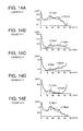
- FIGS. 14A to 14E are diagrams showing results of flatness tests for examples of the embodiment.
- FIGS. 15A to 15E are diagrams showing results of flatness tests for examples of the embodiment.
- FIG. 16 is a diagram showing a result of a flatness test for a comparative example.
- FIGS. 17A and 17B are diagrams showing the configuration of a high-order mode laminated 1 ⁇ 2 wave plate.
- FIG. 18 is an exploded perspective view showing the configuration of a high-order mode laminated 1 ⁇ 2 wave plate as an example of a phase difference plate according to another embodiment of the invention.
- FIG. 19 is a diagram showing a Poincare sphere that illustrates the locus of a polarized state in the laminated 1 ⁇ 2 wave plate shown in FIGS. 17A and 17B .
- FIG. 20 is a diagram illustrating a transition in the orbit of a linearly-polarized light beam in a Poincare sphere in the laminated 1 ⁇ 2 wave plate having the configuration shown in FIG. 18 .
- FIGS. 21A and 21B are diagrams showing the conversion efficiency of the laminated 1 ⁇ 2 wave plate for the range of 400 nm to 700 nm.
- FIGS. 22A and 223 are diagrams showing the conversion efficiency of the laminated 1 ⁇ 2 wave plate for the range of 400 nm to 700 nm.
- FIGS. 23A and 23B are diagrams showing the conversion efficiency of the laminated 1 ⁇ 2 wave plate for the range of 400 nm to 700 nm.
- FIGS. 24A , 24 B, and 24 C are diagrams showing the external appearance of a polarization conversion unit in which the polarization conversion element according to the embodiment of the invention is built.
- FIG. 25 is an exploded perspective view of the polarization conversion unit shown in FIGS. 24A to 24C .
- FIG. 26 is a diagram illustrating a method of fixing the polarization conversion element embodied as shown in FIGS. 5A and 5B .
- FIG. 27 is a diagram illustrating a method of fixing the polarization conversion element embodied as shown in FIGS. 5A and 5B .
- FIG. 28 is a diagram showing a liquid crystal projector as an example of a light projecting apparatus to which a polarization conversion element according to an embodiment of the invention is applied.
- FIG. 29 is a diagram illustrating the configuration of a general polarization conversion element.
- FIG. 30 is a diagram illustrating the configuration of a general polarization conversion element.
- FIG. 1 is a diagram showing an example of a polarization conversion element according to a first embodiment of the invention.
- the polarization conversion element 1 includes an element main body (optical element) 10 as the above-described PBS array and a phase difference plate (laminated 1 ⁇ 2 wave plate) 20 that is selectively bonded to the element main body 10 and is formed from an inorganic optical crystal such as a quartz crystal.
- the inorganic optical crystal such as a quartz crystal has superior thermal conductivity.
- the above-described phase difference plate has superior thermal resistance, and there is no concern about degradation of optical characteristics thereof due to a high temperature.
- lithium tantalate, sapphire, or the like other than the quartz crystal can be used as the material of the phase difference plate.
- the element main body 10 includes a plurality of light transmitting substrates 11 , polarization splitting films (polarization splitting portions) 12 and reflective films (reflective portions) 13 that are alternately disposed between the plurality of light transmitting substrates 11 , and adhesive layers 14 that are disposed between the plurality of light transmitting substrates 11 and bond the light transmitting substrates 11 together.
- the element main body 10 includes a light incident face 16 and a light outgoing face 17 that are approximately parallel to each other.
- the plurality of light transmitting substrates 11 are bonded together by the adhesive layers 14 with the polarization splitting film (polarization splitting portion) 12 and the reflective film (reflective portion) 13 alternately interposed therebetween using bonding faces 11 a that have a predetermined tilt angle with respect to the light incident face 16 or the light outgoing face 17 .
- the polarization splitting film 12 selectively transmits a P-polarized light beam of input light (an S-polarized light beam and a P-polarized light beam) input from the outside and reflects the S-polarized light.
- the reflective film 13 reflects the S-polarized light, which is reflected by the polarization splitting film 12 , toward the light outgoing face 17 .
- the thickness of the adhesive layer 14 is equal to or more than 5 ⁇ m and equal to or less than 10 ⁇ m.
- the adhesive layer 14 is formed by using an ultraviolet-curing type adhesive that has modified acrylate or modified methacrylate as its main component, it can be formed to have the above-described thickness.
- modified acrylate or modified methacrylate is not used as its main component, and accordingly, the viscosity is high, and the thickness of the adhesive layer is equal to or more than 10 ⁇ m and is equal to or less than 20 ⁇ m.
- the thickness of the adhesive layer exceeds 10 ⁇ m
- deformation occurs in the end portion of the adhesive layer. Accordingly, when the light incident face 16 and the light outgoing face 17 are ground ( FIG. 12 ), the corners of the light transmitting substrate 11 , which are near the deformation, are removed. As a result, when the phase difference plate 20 is bonded to the light outgoing face 17 of the light transmitting substrate 11 , a gap is formed between the light transmitting substrate 11 and the phase difference plate 20 so as to generate air bubbles.
- the light transmitting substrate 11 and the phase difference plate 20 are not sufficiently bonded to each other, and the phase difference plate 20 can be easily peeled off.
- the light transmittance decreases due to the air bubbles generated between the light transmitting substrate 11 and the phase difference plate 20 .
- the thickness of the adhesive layer is less than 5 ⁇ m, when a foreign material or the like is mixed in the adhesive layer, the bonding strength of the bonding layer decreases due to the foreign material or the like.
- the thickness of the adhesive layer is equal to or more than 5 ⁇ m and is equal to or less than 10 ⁇ m, it is difficult to remove the corners of the light transmitting substrate 11 , and accordingly, air bubbles are not generated, and easiness in the peel-off of the phase difference plate 20 from the light transmitting substrate 11 and a decrease in light transmittance can be resolved.
- the phase difference plate 20 is bonded to the light outgoing face 17 of the light transmitting substrate 11 above the polarization splitting film 12 by the bonding layer 21 .
- the phase difference plate 20 is a 1 ⁇ 2 wave plate manufactured by using a quartz crystal as described above and converts the P-polarized light beam transmitted through the polarization splitting film 12 into S-polarized light.
- the phase difference plate 20 is disposed above the reflective film 13 .
- the bonding layer 21 is a plasma polymerized film that is formed through a molecular junction, and the main material thereof is polyorganosiloxane.
- the plasma polymerized film is formed by using a plasma polymerization method so as to include a siloxane bond and includes a Si framework of which the degree of crystallization is 45% or less and a leaving group that is formed from an organic group combined with the Si framework. By applying energy so as to allow the leaving group present near the surface to leave the Si framework, the adhesiveness is realized.
- FIGS. 2A and 2B are schematic diagrams illustrating the composition of a plasma-polymerized film.
- FIG. 2A illustrates the composition before energy is applied
- FIG. 2B illustrates the composition after the energy is applied.
- the plasma polymerized film includes a siloxane bond (Si—O) 21 A including a Si framework 21 B and a leaving group 12 C that is bonded with the Si framework 21 B.
- Si—O siloxane bond
- the adhesiveness is implemented on the surface of the bonding layer 21 .
- the bonding layer 21 can be firmly bonded.
- the degree of crystallization of the Si framework 21 B of the bonding layer 21 is equal to or less than 45%, and it is more preferable that the degree of crystallization of the Si framework 21 B is equal to or less than 40%.
- the Si framework 21 B includes a sufficiently random atomic structure, whereby the characteristics of the Si framework 21 B are actualized.
- “being activated” represents a state in which leaving groups 21 C located on the surface and the inside of the bonding layer 21 are detached, and a bond that is not terminated (hereinafter also referred to as a “free bond” or a “dangling bond”) is generated in the Si framework 215 , a state in which a free bond is terminated by a hydroxyl group (OH group), or a state in which such states are mixed.
- a free bond a bond that is not terminated
- OH group hydroxyl group
- the active bond 21 D represents a free bond (dangling bond) or a free bond terminated by a hydroxyl group. According to such an active bond 21 D, firm joining of the bonding layer 21 can be formed.
- the optical characteristics are not influenced by the degradation of the adhesive.
- the bonding layer 21 is formed so as to have no gap by using a plasma polymerization method, whereby the light transmitting substrate 11 and the phase difference plate 20 can be strongly bonded.
- the method of bonding the phase difference plate 20 and the light outgoing face 17 is not limited to the plasma polymerization method, but the phase difference plate 20 and the light outgoing face 17 may be bonded together by using an adhesive that includes modified methacrylate or modified acrylate described above as its main component.
- the bonding layer 21 may be formed by using not only the plasma polymerization method but also an atomic diffusion joining method.
- microcrystalline continuous thin films are formed as films on a light transmitting substrate 11 and a phase difference plate 20 that configure an element main body 10 through vacuum film formation such as sputtering or ion plating inside a vacuum container. Then, the microcrystalline continuous thin films are superimposed during or after the formation of the films, and atomic diffusion is caused to occur on the joining boundary face and the grain boundary, whereby the light transmitting substrate 11 and the phase difference plate 20 are firmly joined.
- microcrystalline continuous thin films are superimposed, but a microcrystalline continuous thin film is formed on one of the light transmitting substrate 11 and the phase difference plate 20 , and a microcrystalline structure is formed on the other, and, by superimposing the microcrystalline continuous thin film and the microcrystalline structure, the atomic diffusion joining can be performed.
- FIG. 3 is an exploded perspective view showing a polarization conversion element according to another embodiment of the invention.
- FIG. 4 is a cross-sectional view showing a part of the polarization conversion element shown in FIG. 3 in an enlarged scale.
- the polarization conversion element shown in FIGS. 3 and 4 includes an element main body 10 as a PBS array and a phase difference plate 20 , which is made of a quartz crystal, that is joined to the element main body 10 , serves as a 1 ⁇ 2 wave plate, rotates the polarizing face of incident linearly-polarized light by 90 degrees, and outputs resultant light.
- the element main body 10 has an approximately rectangular parallelepiped shape, and end portions in the longitudinal direction in which two element main bodies 10 A and 10 B face each other are joined together so as to have symmetry with respect to the joining face 10 C.
- This element main body 10 includes a light incident face 10 D and a light outgoing face 10 E that are approximately parallel to each other.
- the element main body 10 includes polarization splitting films 12 and reflective films 13 that are arranged between a plurality of light transmitting substrates 11 so as to be alternately aligned in the longitudinal direction.
- each one of the plurality of light transmitting substrates 11 is joined by a joining face 11 a that has a predetermined tilt angle with respect to the light incident face 10 D or the light outgoing face 10 E.
- the polarization splitting film 12 and the reflective film 13 are alternately disposed in each boundary portion 11 B between the plurality of light transmitting substrates 11 .
- the polarization splitting film 12 splits light incident to the light incident face 10 D into two types of linearly-polarized light beams of which the polarizing directions are perpendicular to each other, transmits one linearly-polarized light beam, and reflects the other linearly-polarized light.
- the polarization splitting film 12 selectively transmits a P-polarized light beam of random polarized light that is incident to the light incident face 10 D and reflects S-polarized light.
- the reflective film 13 reflects the other linearly-polarized light beam reflected by the polarization splitting film 12 and changes the direction of the optical path thereof. In other words, the reflective film 13 reflects the S-polarized light beam reflected by the polarization splitting film 12 toward the light outgoing face 10 E.
- the element main body 10 as shown in FIG. 4 , includes adhesive layers 14 that join the plurality of light transmitting substrates 11 together.
- the adhesive layer 14 may use an optical-based adhesive of an ultraviolet-curing type or the like.
- an ultraviolet-curing type adhesive is used, the viscosity is high, and the thickness of the adhesive layer 14 is approximately equal to or more than 10 ⁇ m and is equal to or less than 20 ⁇ m.
- the thickness of the adhesive layer 14 can be formed to be as thin as 5 ⁇ m or more and 10 ⁇ m or less.
- ultraviolet-curing adhesive that includes modified acrylate or modified methacrylate as its main component
- the adhesive layer 14 has a predetermined thickness W 1 .
- phase difference plates 20 ( 20 A and 20 B) are arranged on the light outgoing faces 10 E of two element main bodies 10 A and 10 B.
- the phase difference plate 20 rotates the polarization plane of the P-polarized light by 90 degrees by causing the P-polarized light beam transmitted through the polarization splitting film 12 to have a phase difference of 180 (degrees), it converts the P-polarized light beam into a linear polarized light beam that is parallel to the polarized plane of the S-polarized light beam that is reflected by the reflective film 13 , that is, an S-polarized light beam and outputs the S-polarized light.
- the phase difference plate 20 has a comb-like shape (bamboo screen shape).
- the phase difference plate 20 ( 20 A and 20 B) is joined to the element main body 10 and includes a base portion 20 C ( 20 C 1 and 20 C 2 ) through which light is not transmitted and a phase difference portion 20 D ( 20 D 1 and 20 D 2 ) that extends from the base portion 20 C and through which light is transmitted.
- the base portion 20 C is arranged outside an effective area (E) that is an optical area of the element main body 10 .
- the base portions 200 are joined in the longitudinal direction of the base portion 200 , in other words, in a direction in which the polarization splitting film 12 and the reflective film 13 are alternately aligned.
- the base portion 2001 of one phase difference plate 20 A is bonded to one end edge portion 10 F of end edge portions of the element main body 10 that are parallel to the longitudinal direction, and the base portion 2002 of the other phase difference plate 203 approaches the tip end portion 20 E 1 of the phase difference portion 20 D 1 of the one phase difference plate 20 A.
- the base portion 2001 of the one phase difference plate 20 A approaches the tip end portion 20 E 2 of the phase difference portion 20 D 2 of the other phase difference plate 20 B
- the base portion 2002 of the other phase difference plate 20 B approaches the tip end portion 20 E 1 of the phase difference portion 20 D 1 of the one phase difference plate 20 A.
- the base portion 20 C has a principal plane that is in the shape of a long rectangle, and the width thereof, for example, is in the range of about 3 mm to 4 mm.
- the base portion 20 C is joined to the element main body 10 through a joining film not illustrated in the figure.
- This joining film similarly to the adhesive layer 14 , is disposed by using an optical-based adhesive of an ultraviolet-curing type or the like or a plasma polymerized film. Since the joining film is preferably arranged on the outer side of the effect area E that is an optical area not arranged on the optical path, it is preferable that the joining film is formed only between the base portion 200 and the end edge portions 10 F and 10 G that are parallel to the longitudinal direction of the element main body 10 .
- the phase difference plate 20 (phase difference portion 20 D) has a strip shape, and the thickness thereof is the same as that of the base portion 200 .
- the phase difference portion 200 extends from the base portion 200 and is arranged on the light outgoing face 10 E of the element main body 10 in an area located in an upper portion of the polarization splitting film 12 .
- a plurality of the phase difference portions 200 is arranged with a gap W 2 of a predetermined width interposed therebetween, and the S-polarized light beam reflected by the reflective film 13 directly passes through the gap W 2 .
- Each phase difference portion 20 D has the light incident face 20 F that faces the light outgoing face 10 E of the element main body 10 .
- a small gap W 3 is formed between the light incident face 20 F of the phase difference portion 200 and the light outgoing face 10 E of the element main body 10 . Accordingly, it is preferable that anti-reflection films, which are not illustrated in the figure, are formed on the light incident face 20 F of the phase difference portion 200 and the light outgoing face 10 E of the optical element 310 .
- the phase difference portion 200 of the phase difference plate 20 is not bonded to the element main body 10 by using an adhesive, and accordingly, degradation of the optical characteristics due to the degradation of the adhesive can be avoided.
- phase difference portions 20 D is integrated with the base portion 20 C, the assembly of the phase difference plate 20 into the element main body 10 can be easily performed.
- FIGS. 5A and 5B are exploded perspective views showing a polarization conversion element according to a further embodiment of the invention.
- FIG. 5A is an overall perspective view of the polarization conversion element
- FIG. 5B is an assembly diagram illustrating the assembly of the polarization conversion element.
- the polarization conversion element 1 is configured to include a flat plate-shaped element main body 10 , a plurality of phase difference plates 20 , which are formed from quartz crystal members, having strip shapes, and double-sided tapes 25 as two spacer members.
- the double-sided tapes 25 are attached to both end portions of the element main body 10 in the vertical direction (Z direction) on the light beam emitting side face of the flat plate-shaped element main body 10 .
- phase difference plates 20 are placed on the upper faces of the double-sided tapes 25 so as to be coincident with positions corresponding to the polarization splitting films 12 from the upper side (Y direction) of the attached doubled-sided tapes 25 , and the phase difference plates 20 are pressed.
- the polarization conversion element 1 is completed. This assembly process is performed by using an assembly jig.
- An attachment object can be peeled from and re-attached to the double-sided tapes 25 .
- the tape thickness of the double-sided tapes 25 is 0.15 mm.
- the polarization conversion element 1 assembled as above is in the form of being interposed between both end portions of element main body 10 that are located on the light beam outgoing side and both end portions of the phase difference plate 20 that are located on the light beam incident side with the double-sided tape 25 interposed therebetween.
- the double-sided tapes 25 are located at positions outside the effective range of light beams emitted from the light source in the polarization conversion element 1 .
- the manufacturing process is largely configured by a film forming process, a bonding process, a cutting process, and a grinding process.
- FIGS. 6 to 12 are diagrams illustrating the manufacturing process of a polarization conversion element according to this embodiment, particularly, an element main body thereof.
- a plurality of light transmitting substrates (colorless light transmitting substrates formed from glass or the like) 11 A is prepared.
- a light transmitting substrate 11 A includes a first face 11 A 1 and a second face 11 A 2 that are approximately parallel to each other.
- a polarization splitting film 12 is formed on the first face 11 A 1
- a reflective film 13 is formed on the second face 11 A 2 .
- the light transmitting substrate 11 A on which the polarization splitting film 12 and the reflective film 13 are formed and the light transmitting substrate 11 A on which such films are not formed are alternately bonded together by the adhesives 14 A.
- the polarization splitting film 12 and the reflective film 13 are alternately stacked with the light transmitting substrate 11 A interposed therebetween.
- an adhesive that includes modified acrylate or modified methacrylate as its main component is used as the adhesive 14 A, and the coating amount thereof is adjusted such that the thickness after curing is in the range of 5 to 10 ⁇ m.
- ultraviolet light is emitted to the first face 11 A 1 of the light transmitting substrate 11 A in a direction that is approximately perpendicular to the first face 11 A 1 of the light transmitting substrate 11 A.
- the ultraviolet light passes through the polarization splitting film 12 and the reflective film 13 , all the adhesives 14 A shown in FIG. 8 are simultaneously cured.
- the adhesive layers 14 are formed between the polarization splitting film 12 and the light transmitting substrate 11 A and between the reflective film 13 and the second light transmitting substrate.
- a laminated body 400 is formed which is acquired by bonding the plurality of the light transmitting substrates 11 A.
- the ultraviolet light may be emitted from a direction that is approximately parallel to the first face 11 A 1 of the light transmitting substrate 11 A.
- the emission amount of the ultraviolet light is equal to or more than 15,000 mJ/cm 2 and is equal to or less than 45,000 mJ/cm 2 , and more particularly, in a case where the emission amount is equal to or larger than 20,000 mJ/cm 2 and is equal to or smaller than 35,000 mJ/cm 2 , the tensile strength of the adhesive layer 14 is high, which is preferable.
- the tensile strength of the adhesive layer 14 is high, which is preferable.
- the shearing strength of the adhesive layer 14 is high, which is preferable.
- Each curing test was performed twice, which is illustrated in Table 1.
- the tests of the tensile strength and the shearing strength were performed by using the following test method.
- a tension tester By using a tension tester, a tensile weight was applied to a test sample, which was acquired by bonding two white glass plates having a size of 10 mm ⁇ 10 mm together by using an adhesive 14 A, in the vertical direction or in the parallel direction with respect to the bonding face, and the weight at a time when the two white glass plates were separated from each other was measured.
- the laminated body 400 is cut off approximately parallel with the cut face that forms a predetermined angle ⁇ (about 45 degrees) with the first face 11 A 1 , whereby a laminated block 410 is cut out.
- the cut face 410 A of the cut laminated block 410 is ground by a grinding device 500 , whereby the element main body 10 of the polarization conversion element 1 can be acquired.
- the heat resistance of the adhesive was evaluated in Example 1 and Comparative Example 1.
- FIG. 13 is a diagram showing a heat resistance test of Example 1 and Comparative Example 1.
- Example 1 two glass plates were bonded by using an adhesive (UT20; made by Adell Corp.), and a predetermined amount of ultraviolet light was emitted thereto. Accordingly, a test piece 600 of Example 1 was produced.
- an adhesive UT20; made by Adell Corp.
- Comparative Example 1 two glass plates were bonded together by using a general adhesive (PhotoBond 300; manufactured by Sunrise MSI Corp.), and a predetermined amount of ultraviolet light was emitted thereto. Accordingly, a test piece 601 of Comparative Example 1 was produced.
- a general adhesive PhotoBond 300; manufactured by Sunrise MSI Corp.
- test pieces 600 and 601 were fixed within a fixing frame 610 , and the test pieces 600 and 601 were built in a place at which the polarization conversion element of the projector was to be disposed, and the cooling mechanism of the projector was adjusted such that the temperature of the test pieces was 120° C. when light of a light source lamp was emitted to the test pieces 600 and 601 .
- FIG. 13 shows a test result in a case where the test pieces were left under such an environment for 3800 hours.
- the adhesive layer formed by using the adhesive according to the embodiment of the invention has superior heat resistance.
- FIGS. 14A to 14E are diagrams showing results of flatness tests for Examples 2 to 6 of the invention.
- FIGS. 15A to 15E are diagrams showing results of flatness tests for Examples 7 to 11 of the invention.
- FIG. 16 is a diagram showing a result of a flatness test for Comparative Example 2.
- Example 2 an element main body 10 as shown in FIG. 25 to be described later was produced by using the same adhesive as that of Example 1.
- a left element main body 10 out of two element main bodies 10 shown on the left and right sides in FIG. 25 was used.
- a cross-sectional view at the approximate center of the light incident face 16 of the element main body 10 was acquired.
- the cross-sectional view is a cross-sectional view taken along the horizontal direction in FIG. 25 .
- a convex portion that is relatively largely expanded to the upper side is selected, and vertexes of concave portions near the left and right sides of the convex portion are joined with a line. A distance from this line to each vertex of the convex portion was converted into the scale of the vertical axis, and a “height difference” was calculated.
- Example 3 an element main body 10 was produced similarly to Example 2, and the light incident face 16 was measured so as to acquire a cross-sectional view. Then, based on the cross-sectional view, similarly to Example 2, the “height differences” were calculated for two points.
- FIGS. 14A to 14E show such results.
- Examples 7 to 11 for the light outgoing face 17 of the element main body 10 manufactured in Examples 2 to 6, a cross-sectional view was acquired similarly to Example 2. Based on the acquired cross-sectional view, similarly to Example 2, the “height differences” were calculated for two points.
- Comparative Example 2 except for using the same adhesive as that of Comparative Example 1 as an adhesive, the element main body was produced similarly to Example 2, and a cross-sectional view in which the light outgoing face was measured was acquired. Based on the acquired cross-sectional view, similarly to Example 2, the “height differences” were calculated for two points.
- the wavelength of light that is set in the laser interferometer is 685 nm.
- interference fringe analyzing software produced by Fujinon Corp. (currently, Fuji Film Corp.)
- Fujinon Corp. currently, Fuji Film Corp.
- phase difference plate According to an embodiment of the invention, the configuration of a phase difference plate according to an embodiment of the invention will be described.
- FIGS. 17A and 17B are diagrams showing the configuration of a high-order mode laminated 1 ⁇ 2 wave plate (hereinafter, referred to as a laminated 1 ⁇ 2 wave plate) as an example of a phase difference plate according to an embodiment of the invention.
- FIG. 17A is a perspective view
- FIG. 17B is an exploded perspective view.
- the azimuth of the optical axis of the first wave plate 30 is assumed to be ⁇ 1
- the azimuth of the optical axis of the second wave plate 40 is assumed to be ⁇ 2 .
- the azimuth of the optical axis is an angle that is formed by the crystalline optical axis and the polarization plane of linearly-polarized light beam incident to the laminated wave plate.
- cut angles of the first wave plate 30 and the second wave plate 40 are 90 (degrees) Z (an intersection angle between the normal line direction of the principal face of the quartz crystal plate and the optical axis (Z axis) is 90 degrees).
- the laminated 1 ⁇ 2 wave plate 20 is used in the polarization conversion element that is built in a liquid crystal projector
- a phase difference of the first wave plate 30 for a predetermined designed wavelength ⁇ for example, light (green light) of 520 nm
- the phase difference of the second wave plate 40 is ⁇ 2
- the following Equation is satisfied.
- 180(degrees) (1)
- the laminated 1 ⁇ 2 wave plate 20 for a broad band including the wavelength bands (R (red: 400 nm band), G (green: 500 nm band), and B (blue: 675 nm)) that are necessary for a liquid crystal projector, has a polarization conversion efficiency of approximately 0.8 or more and, particularly for the G band, a polarization conversion efficiency of approximately 1.0, and accordingly, a phase difference of 180 (degrees) is required.
- a technique is used in which a phase difference, a conversion efficiency, and the like are acquired by variously changing the phase differences ⁇ 1 and ⁇ 2 of the first and second wave plates 30 and 40 for a predetermined wavelength and the azimuths ⁇ 1 and ⁇ 2 thereof as configuration parameters of the laminated 1 ⁇ 2 wave plate 1 .
- the phase difference for incidence light of a broad band including the above-described three wavelength bands RGB is 180 (degrees), so that the polarization conversion efficiency is approximately 1 by satisfying the following relationship between the azimuth ⁇ 1 of the optical axis of the first wave plate 30 and the azimuth ⁇ 2 of the optical axis of the second wave plate 40 .
- ⁇ 1 45(degrees)
- ⁇ 2 135(degrees)
- ⁇ 2 ⁇ 1 90(degrees)(the azimuths of the optical axes are perpendicular to each other) (4)
- the range of values that can be taken by the design wavelength ⁇ is 490 ⁇ 550 (nm).
- FIG. 18 is an exploded perspective view showing the configuration of a high-order mode laminated 1 ⁇ 2 wave plate as an example of a phase difference plate (hereinafter, referred to as a laminated 1 ⁇ 2 wave plate) according to another embodiment of the invention.
- the azimuth ⁇ 1 of the optical axis of the first wave plate 30 and the azimuth ⁇ 2 of the optical axis of the second wave plate 40 are reversed from those of the case shown in FIGS. 17A and 17B .
- the phase difference for light of a broad wavelength band including the above-described three wavelength bands is 180 (degrees), and the polarization conversion efficiency is approximately “1”.
- the range of values that can be taken by the design wavelength ⁇ is 490 ⁇ 550 (nm).
- I is the polarization state of incidence light
- E is a vector that represents the polarization state of emission light
- R 1 is a Mueller matrix of the first wave plate 30 of the laminated 1 ⁇ 2 wave plate 20
- R 2 is a Mueller matrix of the second wave plate 40 , which are represented by the following Equations.
- R 1 [ 1 0 0 0 0 1 - ( 1 - cos ⁇ ⁇ ⁇ 1 ) sin 2 ⁇ 2 ⁇ ⁇ 1 1 - ( 1 - cos ⁇ ⁇ ⁇ 1 ) sin ⁇ ⁇ 2 ⁇ ⁇ 1 ⁇ cos ⁇ ⁇ 2 ⁇ ⁇ 1 - sin ⁇ ⁇ ⁇ 1 ⁇ sin ⁇ ⁇ 2 ⁇ ⁇ 1 0 ( 1 - cos ⁇ ⁇ ⁇ 1 ) sin ⁇ ⁇ 2 ⁇ ⁇ 1 ⁇ cos ⁇ ⁇ 2 ⁇ ⁇ 1 1 - ( 1 - cos ⁇ ⁇ ⁇ 1 ) sin 2 ⁇ 2 ⁇ ⁇ 1 sin ⁇ ⁇ ⁇ 1 sins ⁇ ⁇ 2 ⁇ ⁇ 1 0 sin ⁇ ⁇ ⁇ 1 ⁇ sin ⁇ ⁇ 2 ⁇ ⁇ 1 sin ⁇ ⁇ 2 ⁇ ⁇ 1 0 sin ⁇ ⁇ ⁇ 1 ⁇ sin ⁇ ⁇ 2 ⁇ ⁇ 1 sin
- phase differences ⁇ 1 and ⁇ 2 of the first and second wave plates 30 and 40 and the azimuths ⁇ 1 and ⁇ 2 of the optical axes are set, and the Mueller matrixes R 1 and R 2 are acquired by using Equations (6) and (7).
- the polarization state E of emission light can be calculated by using Equation (4).
- the polarization state E of emission light is represented by the following Equation.
- phase difference F of the wave plate can be represented by the following Equation.
- n is a positive integer.
- phase difference can be calculated by using Equation (9).
- FIG. 19 is a diagram showing a Poincare sphere that illustrates the locus of a polarized state in the laminated 1 ⁇ 2 wave plate 20 shown in FIGS. 17A and 17B .
- this phase modulation (rotation by 90 (degrees)) modulates light from an incidence polarization state P 0 to P 2 , and a phase difference that is necessary at this time is 180 (degrees).
- the laminated 1 ⁇ 2 wave plate 20 serves as a complete 1 ⁇ 2 wave plate
- P 2 is a point located on the equator that is acquired by rotating P 0 by 180 (degrees).
- the product of the matrix E that represents the polarization state of outgoing light and the matrix P of a polarizer is calculated, and the polarization state is precisely determined by using the acquired amount of light as an evaluation value. This is defined as a conversion efficiency.
- the transmission axis of the matrix P of the polarizer is set to 90 (degrees), and the amount of light of the polarization plane component in the direction of 90 (degrees) can be calculated by using the Stokes parameters of matrix T that are acquired through the product of the matrix P and the matrix E representing the polarization state of outgoing light.
- the product of the matrix E representing the polarization state of outgoing light and the matrix P of the polarizer is as the following equation.
- T the product of the matrix E representing the polarization state E of the outgoing light and the matrix P of the polarizer is denoted by T
- the matrix T represents the conversion efficiency.
- the matrix T is represented by the Stokes parameters of the elements, it can be represented by the following equation.
- S 02 of the Stokes parameters of the vector T represents the amount of light.
- S 02 represents the conversion efficiency.
- the phase difference and the conversion efficiency can be acquired based on the matrix E that represents the polarization state after transmission through the laminated 1 ⁇ 2 wave plate.
- the above-described conversion efficiency was used as an evaluation criterion, and, simulation was performed by using a computer by variously changing the phase differences ⁇ 1 and ⁇ 2 of the first and second wave plates 30 and 40 for a predetermined wavelength (for example, a wavelength of 520 nm) and the azimuths ⁇ 1 and ⁇ 2 of optical axes thereof as various parameters of the laminated 1 ⁇ 2 wave plate.
- a predetermined wavelength for example, a wavelength of 520 nm
- the simulation was repeatedly performed, and the parameters in a case where the conversion efficiency is high for the desired broad wavelength band were selected.
- the ranges of the azimuths ⁇ 1 and ⁇ 2 of optical axes are effective in the range of ⁇ 5 (degrees) from the set angle in accordance with the required specifications or as an allowable error.
- FIG. 20 is a diagram illustrating a Poincare sphere that represents the orbit in the polarized state of the laminated 1 ⁇ 2 wave plate 20 shown in FIG. 18 .
- the phase difference is 180 (degrees), and it is understood that the wave plates serve as a 1 ⁇ 2 wave plate as a whole.
- FIGS. 21A and 21B are diagrams showing the conversion efficiency of the laminated 1 ⁇ 2 wave plate 20 according to the embodiment of the invention for the wavelength range of 400 nm to 700 nm.
- FIG. 21A is a graph diagram showing changes in the polarization conversion efficiency for each wavelength in a case where the designed wavelength ⁇ of each wave plate is 490 nm (G), and the incidence angle is changed from ⁇ 3 (degrees) to +3 (degrees).
- FIG. 21B is a graph diagram showing changes in the polarization conversion efficiency for each wavelength in a case where the designed wavelength ⁇ of each wave plate is 490 nm (G), and the incidence angle is changed from ⁇ 10 (degrees) to +10 (degrees).
- FIGS. 22A and 22B are diagrams showing the conversion efficiency of the laminated 1 ⁇ 2 wave plate 20 according to the embodiment of the invention for the wavelength range of 400 nm to 700 nm.
- FIG. 22A is a graph diagram showing changes in the polarization conversion efficiency for each wavelength in a case where the designed wavelength ⁇ , of each wave plate is 520 nm, and the incidence angle is changed from ⁇ 3 (degrees) to +3 (degrees).
- FIG. 22B is a graph diagram showing changes in the polarization conversion efficiency for each wavelength in a case where the designed wavelength ⁇ of each wave plate is 520 nm, and the incidence angle is changed from ⁇ 10 (degrees) to +10 (degrees).
- the curves are in the state of approximately overlapping each other. Since the wavelengths of blue, green, and red used in a liquid crystal projector are a 400 nm band, a 500 nm band, and a 675 nm band, it was determined that the conversion efficiency of the laminated 1 ⁇ 2 wave plate 1 of the above-described parameters, even in a case where there is a deviation of ⁇ 10 (degrees) in the incidence angle, was equal to or higher than 0.8 in the necessary wavelength band and was approximately 1.0 in the G band.
- FIGS. 23A and 23B are diagrams showing the conversion efficiency of the laminated 1 ⁇ 2 wave plate 20 according to the embodiment of the invention for the wavelength range of 400 nm to 700 nm.
- FIG. 23A is a graph diagram showing changes in the polarization conversion efficiency for each wavelength in a case where the designed wavelength 2 of each wave plate is 550 nm, and the incidence angle is changed from ⁇ 3 (degrees) to +3 (degrees)
- FIG. 23B is a graph diagram showing changes in the polarization conversion efficiency for each wavelength in a case where the designed wavelength ⁇ of each wave plate is 550 nm, and the incidence angle is changed from ⁇ 10 (degrees) to +10 (degrees).
- the curves are in the state of approximately overlapping each other. Since the wavelengths of blue, green, and red used in a liquid crystal projector are a 400 nm band, a 500 nm band, and a 675 nm band, it was determined that the conversion efficiency of the laminated 1 ⁇ 2 wave plate 1 of the above-described parameters, even in a case where there is a deviation of ⁇ 10 (degrees) in the incidence angle, was equal to or higher than 0.8 in the necessary wavelength band of 450 to 700 nm and was approximately 1.0 in the G band.
- the wavelength band to which the laminated 1 ⁇ 2 wave plate responds may be not only RGB but also four wavelengths or five wavelengths acquired by adding the wavelength of another wavelength.
- FIGS. 24A , 245 , and 24 C are diagrams showing the external appearance of a polarization conversion unit in which the polarization conversion element according to the embodiment of the invention is built.
- FIG. 25 is an exploded perspective view of the polarization conversion unit shown in FIGS. 24A to 24C .
- the polarization conversion unit 120 shown in FIGS. 23A , 23 B, and 24 A to 24 C includes a unit frame 200 , the polarization conversion element 1 according to the embodiment of the invention, a light shielding plate 210 , a lens array 220 , and clips 230 . From one opening face (the lower face in FIG. 25 ) of the unit frame 200 , a polarization conversion element 1 including two polarization conversion element main bodies to be described later is inserted, and from the other opening face (the upper face in FIG. 25 ), the light shielding plate 210 and the lens array 220 are inserted in the mentioned order.
- Such optical elements 210 and 220 are pinched by four clips 230 in the vertical two directions in a state in which the optical elements are housed in the unit frame 200 . Since the clip 230 is formed from elastic bodies, it can be easily attached and detached, and each component of the polarization conversion unit 120 can be easily attached to or detached from the unit frame as well.
- a light beam emitted from a light source is incident to the polarization conversion element 1 (particularly, a PBS film to be described later) at a constant angle, and accordingly, the polarization conversion element 1 can be built in the liquid crystal projector in a posture in which PS conversion can be precisely performed.
- FIGS. 26 and 27 are diagrams illustrating a method of fixing the polarization conversion element embodied as shown in FIGS. 5A and 5B .
- FIGS. 26 and 27 are perspective views of the polarization conversion device when viewed from the light beam outgoing side.
- the polarization conversion element 1 is housed (fixed) in a fixing frame 700 shown in FIG. 26 .
- the fixing frame 700 is configured by first fixing frames 710 and second fixing frames 730 .
- the first fixing frames 710 are arranged on the light beam incident side of the polarization conversion element 1 ( FIG. 27 ), and the second fixing frames 730 are arranged on the light beam outgoing side of the polarization conversion element 1 ( FIG. 26 ).
- the first fixing frame 710 forms a frame shape in an approximately rectangular shape in the plan view, and the element main body 10 of the polarization conversion element 1 is bonded and fixed to the inner face side thereof.
- the second fixing frames 730 are arranged on both end portions of the phase difference plate 20 on the light beam outgoing side of the phase difference plate 20 .
- the second fixing frames 730 are configured as pressing plates 731 and 735 formed in a rectangular plate shape.
- the second fixing frames 730 will be referred to as the pressing plates 731 and 735 as is appropriate.
- the polarization conversion element 1 is configured to include a silicon adhesive 740 as an elastic member having elasticity. After the end portions of the phase difference plate 20 are coated with the silicon adhesive 740 , the pressing plates 731 and 735 are placed in arm portions 718 formed in the first fixing frames 710 from the upper side that is coated with the silicon adhesive 740 , and the polarization conversion element 1 is configured to be fixed to the arm portions 718 by using flange screws 750 ( FIG. 26 ).
- FIG. 28 is a diagram showing a liquid crystal projector as an example of a light projecting apparatus to which a polarization conversion element according to an embodiment of the invention is applied.
- the projection-type display apparatus (liquid crystal projector) 100 shown in FIG. 28 includes an illumination optical system that is configured by a light source 110 , a first lens array 111 , a polarization conversion unit 120 in which the polarization conversion element according to the embodiment of the invention is built, and an overlapping lens 121 .
- the projection-type display apparatus 100 includes a color light splitting optical system 130 that includes dichroic mirrors 131 and 132 and a reflective mirror 133 .
- a light guiding optical system is included therein which includes an incident side lens 140 , a relay lens 141 , and reflective mirrors 142 and 143 .
- the projection-type display apparatus 100 includes three field lenses 144 , 145 , and 146 , three liquid crystal light valves 150 R, 150 G, and 150 B, a cross dichroic prism 160 , and a projection lens 170 .
- the reflective mirror 146 has a function of reflecting light output from the overlapping lens 121 in a direction of the color light splitting optical system 130 .
- the color light splitting optical system 130 has a function of splitting light output from the overlapping lens 121 into three color light beams of red, green, and blue by using two dichroic mirrors 131 and 132 .
- the first dichroic mirror 131 transmits a red light component out of light output from the overlapping lens 121 and reflects a blue light component and a green light component.
- the red light transmitted through the first dichroic mirror 131 is reflected by the reflective mirror 133 , passes through the field lens 144 , and arrives at a red light liquid crystal light value 150 R.
- This field lens 144 converts partial light beams output from the overlapping lens 121 into light beams parallel to the center axis (main light beams).
- the field lenses 145 and 146 disposed before the other liquid crystal light valves operate similarly.
- the green light is reflected by the second dichroic mirror 132 , passes through the field lens 145 , and arrives at the green light liquid crystal light valve 150 G.
- the blue light is transmitted through the second dichroic mirror 132 , passes through the light guiding optical system, that is, the incident-side lens 140 , the reflective mirror 142 , the relay lens 141 , and the reflective mirror 143 , further passes through the field lens 146 , and arrives at the blue light liquid crystal light valve 150 B.
- the reason for using the light guiding optical system for the blue light is to prevent a decrease in the use efficiency of light due to diffusion of light and the like that is caused by the length of the optical path of the blue light that is longer than that of the other color light.
- the reason is for directly transmitting the light beam incident to the incident-side lens 140 to the field lens 146 .
- Three liquid crystal light valves 150 R, 150 G, and 150 E have a function as an optical modulation unit that modulates incident light based on given image information (image signal). Accordingly, each color light incident to the three liquid crystal light valves 150 R, 150 G, and 150 B is modulated based on given image information so as to form images of each color light.
- the modulated light of three colors output from the three liquid crystal light valves 150 R, 150 G, and 150 B is incident to the cross-dichroic prism 160 .
- the cross dichroic prism 160 has a function of forming a color image by composing modulated light of three colors as a color light composing unit.
- a dielectric multi-layer film that reflects red light and a dielectric multi-layer film that reflects blue right are formed in an approximate “X” on the boundary face of four rectangular prisms. Through such dielectric multiple-layer film, modulated light of three colors is composed, and composite light used for projecting a color image is formed.
- the composed light generated by the cross-dichroic prism 160 is output in the direction of the projection lens 170 .
- the projection lens 170 has a function of projecting the composed light onto a projection screen and displays a color image on the projection screen.
- the liquid crystal projector by building a polarization conversion unit including a polarization conversion element according to an embodiment of the invention, which has superior heat-resistance and light resistance, in a liquid crystal projector, the liquid crystal projector is acquired which can project a clear image for a long time by using a high-luminance and high-heat dissipating light source.
- the polarization conversion element includes a phase difference plate (laminated 1 ⁇ 2 wave plate) that reliably serves as a 1 ⁇ 2 wave plate for a plurality of mutually different wavelength bands, and accordingly, the liquid crystal projector can be realized which can project a clear image with high luminance.
- a phase difference plate laminated 1 ⁇ 2 wave plate
Landscapes
- Physics & Mathematics (AREA)
- General Physics & Mathematics (AREA)
- Optics & Photonics (AREA)
- Polarising Elements (AREA)
- Liquid Crystal (AREA)
- Projection Apparatus (AREA)
Abstract
Description
| TABLE 1 | |||
| CURING CONDITION | STRENGTH TEST | ||
| CURING | AMOUNT OF UV | TENSILE | SHEARING | |
| TEST | RADIATION (mJ/cm2) | | STRENGTH | |
| 1 | 319 | 80.9910 | 205.4220 |
| 60.8006 | 297.7320 | ||
| 2 | 14,419 | 198.2330 | 343.6190 |
| 389.2000 | 378.9010 | ||
| 3 | 28,519 | 385.3000 | 413.4440 |
| 450.9440 | 313.5120 | ||
| 4 | 42,619 | 164.2760 | 343.5930 |
| 325.8500 | 407.4280 | ||
| 5 | 70,819 | 229.9720 | 328.8330 |
| 198.2580 | 282.4610 | ||
| 6 | 22,504 | 455.7880 | 194.4600 |
| 425.1200 | 252.9660 | ||
| 7 | 44,689 | 310.5040 | 476.2840 |
| 365.3900 | 324.6270 | ||
|Γ1−Γ2|=180(degrees) (1)
θ1=45(degrees) (2)
θ2=135(degrees) (3)
θ2−θ1=90(degrees)(the azimuths of the optical axes are perpendicular to each other) (4)
E=R2·R1·I (5)
T=P·E (10)
Claims (18)
Applications Claiming Priority (2)
| Application Number | Priority Date | Filing Date | Title |
|---|---|---|---|
| JP2011-093779 | 2011-04-20 | ||
| JP2011093779A JP2012226121A (en) | 2011-04-20 | 2011-04-20 | Polarization conversion element, polarization conversion unit, and projection device |
Publications (2)
| Publication Number | Publication Date |
|---|---|
| US20120268718A1 US20120268718A1 (en) | 2012-10-25 |
| US8764197B2 true US8764197B2 (en) | 2014-07-01 |
Family
ID=47021099
Family Applications (1)
| Application Number | Title | Priority Date | Filing Date |
|---|---|---|---|
| US13/439,136 Active 2033-01-10 US8764197B2 (en) | 2011-04-20 | 2012-04-04 | Polarization conversion element, polarization converting unit, and projecting apparatus |
Country Status (2)
| Country | Link |
|---|---|
| US (1) | US8764197B2 (en) |
| JP (1) | JP2012226121A (en) |
Cited By (4)
| Publication number | Priority date | Publication date | Assignee | Title |
|---|---|---|---|---|
| US20220155490A1 (en) * | 2018-03-20 | 2022-05-19 | Invensas Bonding Technologies, Inc. | Direct-bonded lamination for improved image clarity in optical devices |
| US12153222B2 (en) | 2019-12-17 | 2024-11-26 | Adeia Semiconductor Bonding Technologies Inc. | Bonded optical devices |
| US12199082B2 (en) | 2017-03-16 | 2025-01-14 | Adeia Semiconductor Technologies Llc | Method of direct-bonded optoelectronic devices |
| US12271032B2 (en) | 2018-02-26 | 2025-04-08 | Adeia Semiconductor Bonding Technologies Inc. | Integrated optical waveguides, direct-bonded waveguide interface joints, optical routing and interconnects |
Families Citing this family (8)
| Publication number | Priority date | Publication date | Assignee | Title |
|---|---|---|---|---|
| JP6413366B2 (en) * | 2014-06-09 | 2018-10-31 | セイコーエプソン株式会社 | Polarization conversion element and projector |
| US9778475B2 (en) | 2014-11-06 | 2017-10-03 | The United States of America as represesnted by the Secretary of the Air Forice | Universal polarization converter |
| CN105842923A (en) * | 2016-06-02 | 2016-08-10 | 京东方科技集团股份有限公司 | Backlight module and display device |
| US10401639B2 (en) * | 2016-08-12 | 2019-09-03 | Avegant Corp. | Method and apparatus for an optical path length extender |
| JP2019066837A (en) * | 2017-09-29 | 2019-04-25 | キヤノン株式会社 | Polarization separation element and image projection apparatus using the same |
| JP7103159B2 (en) * | 2018-10-29 | 2022-07-20 | コニカミノルタ株式会社 | Optical characterization method and optical characterization system |
| CN109782454A (en) * | 2018-12-17 | 2019-05-21 | 重庆爱奇艺智能科技有限公司 | A polarization conversion device |
| CN211506152U (en) * | 2019-12-31 | 2020-09-15 | 深圳光峰科技股份有限公司 | Polarization beam splitting device, polarization beam splitting structure and projection equipment |
Citations (18)
| Publication number | Priority date | Publication date | Assignee | Title |
|---|---|---|---|---|
| JPS58189605A (en) | 1982-04-28 | 1983-11-05 | Nippon Dempa Kogyo Co Ltd | Combination wavelength plate |
| JPS58194004A (en) | 1982-05-10 | 1983-11-11 | Toyo Commun Equip Co Ltd | Superposition type phase plate |
| JPS58203404A (en) | 1982-05-22 | 1983-11-26 | Nippon Dempa Kogyo Co Ltd | Production of combinational wavelength plate |
| JPS5962807A (en) | 1982-10-04 | 1984-04-10 | Toyo Commun Equip Co Ltd | Superposed phase plate |
| JP2000298212A (en) | 1996-07-25 | 2000-10-24 | Seiko Epson Corp | Optical element, method of manufacturing the same, and projection display device |
| JP2002139703A (en) | 2000-10-31 | 2002-05-17 | Mitsubishi Electric Corp | Wave plate and semiconductor laser using the same |
| JP3309846B2 (en) | 1996-03-12 | 2002-07-29 | セイコーエプソン株式会社 | Method of manufacturing polarization separation device and polarization conversion device |
| US6811262B2 (en) * | 2000-06-28 | 2004-11-02 | Seiko Epson Corporation | Projector comprising an optical component having a rock crystal member |
| US7011412B2 (en) * | 2002-03-28 | 2006-03-14 | Seiko Epson Corporation | Polarization converter, an illumination optical device having the polarization converter and projector |
| US7086737B2 (en) * | 2003-07-15 | 2006-08-08 | Seiko Epson Corporation | Optical apparatus, and projector |
| US7130120B2 (en) * | 2001-10-01 | 2006-10-31 | Sony Corporation | Prism, projection and optical component |
| JP2009103863A (en) | 2007-10-23 | 2009-05-14 | Epson Toyocom Corp | Retardation plate and projector |
| JP4329852B2 (en) | 2007-07-11 | 2009-09-09 | セイコーエプソン株式会社 | Polarization conversion unit, polarization conversion device, and projector |
| JP2010107912A (en) | 2008-10-31 | 2010-05-13 | Epson Toyocom Corp | Laminated quarter wave plate |
| US7764354B2 (en) * | 2001-08-24 | 2010-07-27 | Asahi Glass Company, Limited | Multi-layer diffraction type polarizer and liquid crystal element |
| US20110187999A1 (en) * | 2010-01-29 | 2011-08-04 | Hitachi Consumer Electronics Co., Ltd. | Projection type display apparatus |
| US8031401B2 (en) * | 2006-04-10 | 2011-10-04 | Epson Toyocom Corporation | Laminated half-wave plate, polarizing converter, polarized light illumination device and light pickup device |
| US8186832B2 (en) * | 2008-08-18 | 2012-05-29 | Seiko Epson Corporation | Projector having polarization conversion element array and light shielding sections provided thereon |
Family Cites Families (6)
| Publication number | Priority date | Publication date | Assignee | Title |
|---|---|---|---|---|
| JP5088707B2 (en) * | 2006-04-10 | 2012-12-05 | セイコーエプソン株式会社 | Laminated wave plate, polarization converter, polarization illumination device, and optical pickup device |
| JP2008185768A (en) * | 2007-01-30 | 2008-08-14 | Sony Corp | Wave plate and optical device |
| JP2009035721A (en) * | 2007-07-11 | 2009-02-19 | Seiko Epson Corp | Substrate with bonding film, bonding method and bonded body |
| JP5401661B2 (en) * | 2008-08-22 | 2014-01-29 | 株式会社ムサシノエンジニアリング | Atomic diffusion bonding method and structure bonded by the above method |
| JP5458545B2 (en) * | 2008-10-22 | 2014-04-02 | セイコーエプソン株式会社 | Method for manufacturing optical article |
| JP2010128425A (en) * | 2008-12-01 | 2010-06-10 | Seiko Epson Corp | Polarization converter, lighting device, and projector |
-
2011
- 2011-04-20 JP JP2011093779A patent/JP2012226121A/en not_active Withdrawn
-
2012
- 2012-04-04 US US13/439,136 patent/US8764197B2/en active Active
Patent Citations (18)
| Publication number | Priority date | Publication date | Assignee | Title |
|---|---|---|---|---|
| JPS58189605A (en) | 1982-04-28 | 1983-11-05 | Nippon Dempa Kogyo Co Ltd | Combination wavelength plate |
| JPS58194004A (en) | 1982-05-10 | 1983-11-11 | Toyo Commun Equip Co Ltd | Superposition type phase plate |
| JPS58203404A (en) | 1982-05-22 | 1983-11-26 | Nippon Dempa Kogyo Co Ltd | Production of combinational wavelength plate |
| JPS5962807A (en) | 1982-10-04 | 1984-04-10 | Toyo Commun Equip Co Ltd | Superposed phase plate |
| JP3309846B2 (en) | 1996-03-12 | 2002-07-29 | セイコーエプソン株式会社 | Method of manufacturing polarization separation device and polarization conversion device |
| JP2000298212A (en) | 1996-07-25 | 2000-10-24 | Seiko Epson Corp | Optical element, method of manufacturing the same, and projection display device |
| US6811262B2 (en) * | 2000-06-28 | 2004-11-02 | Seiko Epson Corporation | Projector comprising an optical component having a rock crystal member |
| JP2002139703A (en) | 2000-10-31 | 2002-05-17 | Mitsubishi Electric Corp | Wave plate and semiconductor laser using the same |
| US7764354B2 (en) * | 2001-08-24 | 2010-07-27 | Asahi Glass Company, Limited | Multi-layer diffraction type polarizer and liquid crystal element |
| US7130120B2 (en) * | 2001-10-01 | 2006-10-31 | Sony Corporation | Prism, projection and optical component |
| US7011412B2 (en) * | 2002-03-28 | 2006-03-14 | Seiko Epson Corporation | Polarization converter, an illumination optical device having the polarization converter and projector |
| US7086737B2 (en) * | 2003-07-15 | 2006-08-08 | Seiko Epson Corporation | Optical apparatus, and projector |
| US8031401B2 (en) * | 2006-04-10 | 2011-10-04 | Epson Toyocom Corporation | Laminated half-wave plate, polarizing converter, polarized light illumination device and light pickup device |
| JP4329852B2 (en) | 2007-07-11 | 2009-09-09 | セイコーエプソン株式会社 | Polarization conversion unit, polarization conversion device, and projector |
| JP2009103863A (en) | 2007-10-23 | 2009-05-14 | Epson Toyocom Corp | Retardation plate and projector |
| US8186832B2 (en) * | 2008-08-18 | 2012-05-29 | Seiko Epson Corporation | Projector having polarization conversion element array and light shielding sections provided thereon |
| JP2010107912A (en) | 2008-10-31 | 2010-05-13 | Epson Toyocom Corp | Laminated quarter wave plate |
| US20110187999A1 (en) * | 2010-01-29 | 2011-08-04 | Hitachi Consumer Electronics Co., Ltd. | Projection type display apparatus |
Cited By (5)
| Publication number | Priority date | Publication date | Assignee | Title |
|---|---|---|---|---|
| US12199082B2 (en) | 2017-03-16 | 2025-01-14 | Adeia Semiconductor Technologies Llc | Method of direct-bonded optoelectronic devices |
| US12271032B2 (en) | 2018-02-26 | 2025-04-08 | Adeia Semiconductor Bonding Technologies Inc. | Integrated optical waveguides, direct-bonded waveguide interface joints, optical routing and interconnects |
| US20220155490A1 (en) * | 2018-03-20 | 2022-05-19 | Invensas Bonding Technologies, Inc. | Direct-bonded lamination for improved image clarity in optical devices |
| US12270970B2 (en) * | 2018-03-20 | 2025-04-08 | Adeia Semiconductor Bonding Technologies Inc. | Direct-bonded lamination for improved image clarity in optical devices |
| US12153222B2 (en) | 2019-12-17 | 2024-11-26 | Adeia Semiconductor Bonding Technologies Inc. | Bonded optical devices |
Also Published As
| Publication number | Publication date |
|---|---|
| US20120268718A1 (en) | 2012-10-25 |
| JP2012226121A (en) | 2012-11-15 |
Similar Documents
| Publication | Publication Date | Title |
|---|---|---|
| US8764197B2 (en) | Polarization conversion element, polarization converting unit, and projecting apparatus | |
| US7553025B2 (en) | Projection type image display apparatus, and optical unit and polarization splitting unit each used for the apparatus | |
| US7255444B2 (en) | Optical unit and projection-type image display apparatus using the same | |
| US20080198333A1 (en) | Polarization beam splitter and projection apparatus having the same | |
| CN102809775B (en) | Polarization converting element, polarization converting unit, and projection-type imaging device | |
| US9151960B2 (en) | Polarization conversion element, polarization conversion unit, projection apparatus, and method for manufacturing polarization conversion element having a thin ultraviolet light curing adhesive layer | |
| US8955977B2 (en) | Projection-type image display apparatus | |
| JPH04212102A (en) | Dichroic mirror and projection display device using the mirror | |
| JP6181606B2 (en) | Polarization conversion element and optical apparatus | |
| US6991334B2 (en) | Polarization beam splitting optical system | |
| CN102608747A (en) | Polarization conversion device, polarization conversion unit, and projection type video apparatus | |
| JP2013025065A (en) | Wave plate, polarization conversion element, polarization conversion unit and projection device | |
| JP2012078436A (en) | Wavelength plate and polarizing conversion element, illumination optical system, and image display device using the same | |
| JP2012226240A (en) | Polarization conversion element, polarization conversion unit, and projection device | |
| US7198371B2 (en) | Image displaying apparatus | |
| JP2013003368A (en) | Polarization conversion element, polarization conversion unit and projection device | |
| JP2013025064A (en) | Wave plate, polarization conversion element, polarization conversion unit and projection device | |
| US20060274274A1 (en) | Projection type display apparatus and optical unit used therefor | |
| JP5583558B2 (en) | Polarization conversion illumination device and display device using the same | |
| CN204331253U (en) | Projection display device | |
| JP2013003491A (en) | Polarization conversion element, polarization conversion unit and projection device | |
| JP2012220908A (en) | Polarization conversion element, polarization conversion unit, and projection device | |
| JP2012133269A (en) | Wavelength plate, polarization conversion element, polarization conversion unit and projection device | |
| JP2012226031A (en) | Polarization conversion element, polarization conversion unit, and projection device | |
| JP2009128568A (en) | Polarization conversion element and projector |
Legal Events
| Date | Code | Title | Description |
|---|---|---|---|
| AS | Assignment |
Owner name: SEIKO EPSON CORPORATION, JAPAN Free format text: ASSIGNMENT OF ASSIGNORS INTEREST;ASSIGNOR:KOBAYASHI, SHUHO;REEL/FRAME:027993/0090 Effective date: 20120316 |
|
| STCF | Information on status: patent grant |
Free format text: PATENTED CASE |
|
| MAFP | Maintenance fee payment |
Free format text: PAYMENT OF MAINTENANCE FEE, 4TH YEAR, LARGE ENTITY (ORIGINAL EVENT CODE: M1551) Year of fee payment: 4 |
|
| MAFP | Maintenance fee payment |
Free format text: PAYMENT OF MAINTENANCE FEE, 8TH YEAR, LARGE ENTITY (ORIGINAL EVENT CODE: M1552); ENTITY STATUS OF PATENT OWNER: LARGE ENTITY Year of fee payment: 8 |
|
| MAFP | Maintenance fee payment |
Free format text: PAYMENT OF MAINTENANCE FEE, 12TH YEAR, LARGE ENTITY (ORIGINAL EVENT CODE: M1553); ENTITY STATUS OF PATENT OWNER: LARGE ENTITY Year of fee payment: 12 |