US8755751B2 - Wireless communication apparatus having modulated Tx clock spur control - Google Patents
Wireless communication apparatus having modulated Tx clock spur control Download PDFInfo
- Publication number
- US8755751B2 US8755751B2 US13/574,912 US201113574912A US8755751B2 US 8755751 B2 US8755751 B2 US 8755751B2 US 201113574912 A US201113574912 A US 201113574912A US 8755751 B2 US8755751 B2 US 8755751B2
- Authority
- US
- United States
- Prior art keywords
- wireless telecommunication
- telecommunication apparatus
- frequency
- clocking
- modulated
- Prior art date
- Legal status (The legal status is an assumption and is not a legal conclusion. Google has not performed a legal analysis and makes no representation as to the accuracy of the status listed.)
- Active, expires
Links
Images


Classifications
-
- H—ELECTRICITY
- H04—ELECTRIC COMMUNICATION TECHNIQUE
- H04B—TRANSMISSION
- H04B15/00—Suppression or limitation of noise or interference
- H04B15/02—Reducing interference from electric apparatus by means located at or near the interfering apparatus
Definitions
- the invention relates to the field of wireless communications and more particularly to a wireless communication apparatus including clock spur control.
- ICs Integrated Circuits
- RF Radio Frequency
- BB baseband
- PMU Power Management Unit
- FIG. 1 illustrates the general architecture of a multiple-band 2G/3G phone 100 consisting of a quad band 2.75G (EGPRS), triple band 3G (HSPA+) with 3G receive diversity.
- EGPRS quad band 2.75G
- HSPA+ triple band 3G
- FIG. 1 shows the following components which are typical of a modern mobile:
- RF Front-End circuit 110 supports quad band 2G (Band II, III, V, VIII EGPRS), triple band 3G (WCDMA I, II, III) which is typical of recent mobile phone architecture, the selection of the particular mode/band being performed by means of an antenna switch 111 which directs the signal to the appropriate set of front end filters 112 .
- antenna switch 101 directs the transmit signal generated by the appropriate 2G or 3G Power amplifiers, respectively 113 and 114 , to the antenna.
- 2/3G transceiver 120 includes the conventional circuits required for achieving a 2G or 3G mobile communication, such as, in the receiving chain, Low Noise amplifiers (LNA) 121 , a Rx VCO Frequency synthesizer 122 with appropriate division circuits (represented by local divider LO Div), a circuit 123 achieving programmable Gain amplifier (PGA), Analog to digital converter (ADC) as well as DSP processing.
- transceiver 120 includes a circuit 126 achieving PGA, Digital to Analog (DAC) conversion as well as DSP processing, a Tx VCO frequency synthesizer 125 associated with dividing circuits (LO Div), and conventional digitally controlled Gain amplifier 124 .
- Transceiver 120 further includes appropriate timing circuits 126 as well as a RF-BB baseband interface 127 for interfacing the baseband 130 .
- RFBBi_EN the different control, data and clock signals which are represented in FIG. 1 (such as RFBBi_EN, RX data 1 , RX data 2 , TX data 1 , SYSCLKEN, SYSCLK) are conventional and known to the skilled man and do not need any further discussion.
- baseband 130 achieves communication between the transceiver 120 (through interface 127 ) with different devices and peripherals, such as two cameras 160 , two displays 170 , a USB device 180 through appropriate data and control leads (including CLK clocks and Chip Select CSi) as well as external DDR memory.
- devices and peripherals such as two cameras 160 , two displays 170 , a USB device 180 through appropriate data and control leads (including CLK clocks and Chip Select CSi) as well as external DDR memory.
- PA Power Amplifier
- the RF transmit modulator chain is victim of a digital aggressor activity creating clock and/or data activity related frequency spurs.
- Such aggressor might be, for instance and without any limitation, the camera interface(s) digital bit stream and associated clock, the display interface(s) digital bit stream and associated clock, the USB port, the external memory data and clock bus, Power management Unit (PMU) internal clocks, digital Baseband clock spurs etc. . . .
- PMU Power management Unit
- FIG. 1 the DDR memory 150 , the cameras 160 , the display 170 , the USB interface 180 etc. . . . which pollute the “victim” being the RF block of 2G/3G RF transceiver 120 .
- the pollution of the transmitter block of the RF chain results in modulation of the noise generated by EMI contributors through the uplink transmission carrier, thus causing pollution to the RF receiver of the same mobile phone or even the RF receivers of the other mobiles located in a close vicinity.
- TDI Time Division Isolation
- the TDI can clearly be used in the case of GSM showing bursted access to the RF transceiver . . . however, 3 G communications are full duplex and further requires continuous use of both the RF transmitter and the RF receiver, thus preventing any possibility of TDI.
- the TDI technique does not prevent the emitter of one mobile, for instance a first mobile emitting in the uplink to its base station, to spoil the receiver of a second mobile located in the neighborhood of said first mobile, when the second is receiving in downlink from its own base station.
- a wireless telecommunication apparatus comprising:
- the general control unit uses one of the following information for determining the clocking frequency to be used for the individual component:
- the central control unit controls the clocking frequency of a memory storage, such as a DDR storage.
- the central control unit also controls the clocking of a display interface, a USB interface, a camera interface.
- a master clock is used which is based on a high frequency of 4992 Mhz.
- control of the clocking frequency is based on the use of a programmable divider based on a fixed ratio divider associated with a sigma-delta conversion.
- the invention is particularly suitable for achieving a 2G, 3G or LTE mobile phone incorporate highly sophisticated multimedia functionalities. Alternatively, it can be used for carrying out a Portable Document Assistant.
- FIG. 1 shows an illustrative architecture of a mobile telephone including RF transceiver and different peripherals.
- FIGS. 2 a and 2 b illustrates the basic spectral properties of two particular aggressors in the case of continuous clock harmonics and pulsed clock source.
- FIG. 3 particularly illustrates the generation of spurs coupled to the RF transmitter chain resulting from a DDR storage being clocked at a frequency of 65 Mhz.
- FIG. 3 shows two RF spectra: top line shows the RF transmitter spectrum (ie the victim's spectrum) modulated by the DDR clock spurs (the aggressor) observed in RF RX band of GSM900. Bottom line shows the same RF spectrum with the aggressor and the victim being isolated in the time domain (using TDI).
- FIG. 4 particularly illustrates the generation of spurs coupled to the RF transmitter chain resulting from a DDR storage being clocked at a frequency of 78 Mhz.
- FIG. 3 shows two RF spectra: top line shows the RF transmitter spectrum (ie the victim's spectrum) modulated by the DDR clock spurs (the aggressor) observed in RF RX band of GSM900. Bottom line shows the same RF spectrum with the aggressor and the victim being isolated in the time domain (using TDI).
- FIG. 5 illustrates the respective position of the different modulated Tx clock spurs in the case of a GSM900 communication and a 65 Mhz grid
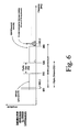
- FIG. 6 illustrates the control of the modulated Tx clock spurs for the case of large DD/DG ratios.
- FIG. 7 illustrates the control of the modulated Tx clock spurs for the case of small DD/DG ratios.
- FIG. 8 illustrates one embodiment of a clocking architecture which allows dynamic control of the modulated Tx clock spurs in accordance with one embodiment.
- clocking architecture which will be described is suitable for allowing combination of wide number of features and functions such as mentioned above, but can also be used for a limited subset of functionalities.
- each individual component or functional entity which is incorporated into a mobile phone has its own clock signal which is generated by one Phase Locked loops so that, in the whole phone, no less than 10 PLLs can be simultaneously (and asynchronously) operated, each one corresponding to its particular functional entity.
- FIGS. 2 a and 2 b The clocking of all those individual components—or aggressors—result in the generation of EMI interference in the receive band.
- Aggressor's basic spectral properties are illustrated in FIGS. 2 a and 2 b as follows:
- FIG. 2 a continuous clock harmonics
- FIG. 2 b pulsed clock source.
- the DDR storage conventionally clocked at a frequency of 104 Mhz—shows to be a critical contributor of EMI interference and thus generates a high number of spurs. Those are unfortunately introduced within the transmission band and might thus spoil the RF receiver of the apparatus or even a RF receiver of a neighboring mobile.
- FIG. 3 particularly illustrates the situation of a DDR storage being clocked at a frequency of 65 Mhz, and which is coupled to a RF transmitter operating at a frequency of 880.2 Mhz.
- a DDR storage being clocked at a frequency of 65 Mhz, and which is coupled to a RF transmitter operating at a frequency of 880.2 Mhz.
- the profile of the Rx band (between 910 Mhz and 970 Mhz) in the two situations where the aggressor is idle (Aggressor OFF during call) and in operation (Aggressor ON at 65 Mhz clock rate).
- FIG. 4 shows the same chart in the case of a DDR storage which is now operated at a frequency of 78 Mhz.
- a DDR storage which is now operated at a frequency of 78 Mhz.
- the violation of the ETSI compliance specification now occurs at a frequency of 78 Mhz above the Tx channel.
- one embodiment of the invention uses a dynamic control of the clocking of the latter so as to ensure that the spurs do not fall into the Rx band.
- the clocking of the DDR is dynamically updated so as to avoid, again, that the spurs deriving from the DDR storage clocking fall into the Rx band.
- any other individual “aggressor”, including the cameras 160 , the display 170 , the USB interface 180 etc. . . . which are likely to generate—through the modulation of the considered Tx transmission—spurs into the Rx band are clocked at a frequency which is dynamically changed in accordance with the value of the Tx transmission carrier.
- the clocking of the individual components is also defined in accordance of:
- FIG. 5 illustrates the respective position of the different modulated Tx clock spurs in the case of a GSM900 communication and a 65 Mhz grid (corresponding to a DDR storage operating at 65 Mhz):
- the Duplex Gap (DG) is being equal to 10 Mhz and the Duplex Distance (DD) is set to 45 Mhz.
- DD Duplex Distance
- FIG. 6 particularly illustrates the control of the position of the modulated Tx clock spurs in the case of a large DD/DG ratio.
- FIG. 7 particularly illustrate the control of the position of the modulated Tx clock spurs in the case of a small DD/DG ratio, such as, for instance in the case of UMTS band IV.
- a small DD/DG ratio such as, for instance in the case of UMTS band IV.
- the modulated Tx clock spurs occur at values being 1772.4 Mhz, . . . 2108.4 Mhz, 2156.4 Mhz, that is to say out of the to receiving band [2110-2155 Mhz].
- each individual aggressor, or contributor to RFI noise within the Tx transmission block can be clocked at one individual frequency which can be controlled so as to continuously remain out of the Rx band being considered.
- all components and more generally all peripherals which are identified to contribute to the generation of spurs within the transmission band are clocked by a controllable clocking system which is under control of one single centralized control unit—a so-called Use Case Manager (UCM) which, in accordance with one embodiment, has high-level vision of the contextual operations of the mobile telephone, and particularly any frequency switching of the RF transmitter controlled by the base station, so as to precisely generate the appropriate control parameters for controlling the different clocks required by the different elements
- UCM Use Case Manager
- the so-called Use Case Manager detects:
- the USC can provide adequate control information for all the frequency dividers generating the different clocks required by the to individual aggressors so as to particularly adjust the clocking in critical cases. For instance, if the USB interface is not being used, the USC will control the frequency division so as to use the default clocking frequency etc. . . .
- FIG. 8 illustrates one particular and illustrative embodiment of a whole clocking architecture which allows dynamic control of the modulated Tx clock spurs in accordance with one embodiment.
- the architecture is based on at least one master clock reference, such as a first high frequency master reference operating at f VCO , operating at a frequency between about 4 and 5 Ghz, and which can be used for generating all or most of the clocks used by the different constituents of the mobile phone, including the possible aggressors.
- a master clock reference such as a first high frequency master reference operating at f VCO , operating at a frequency between about 4 and 5 Ghz, and which can be used for generating all or most of the clocks used by the different constituents of the mobile phone, including the possible aggressors.
- PLL Phase Locked Loop
- oscillator 102 operating at f VCO the output of which being connected to the input of a a programmable divider by N circuit 103 and which output is connected to the a first input of a phase comparator circuit 104 , a second input of which receives the output of a 26 MHz reference crystal oscillator 105 .
- this conventional PLL architecture may rely upon integer N or fractional N division ratios.
- the PLL comprising blocks 101 , 102 , 103 , and 104 is used for generating all frequency clock references, particularly required by the baseband (or also entitled “CPU”), the memory (or also known as “DDR”) and display etc. . . .
- the f VCO frequency is divided by a programmable divider 106 which allows any division between N to N 1 so as to provide a so called variable Digital clock which can be further divided by a dedicated programmable divider 107 used for clocking the Digital Signal Processor (DSP) or also called “Central Processing Unit” (CPU), as well as the divider 107 to feed the external DDR memory, the divider 109 to feed the camera interfaces etc. . . .
- DSP Digital Signal Processor
- CPU Central Processing Unit
- programmable division ratios N 1 , N 2 of divider 106 , P 1 of divider 107 , P 2 of divider 108 and P 3 of divider 109 can be either implemented in integer N or as fractional division ratios depending on the mobile phone application (number of bands, number of telecommunication standards being supported, etc. . . . ).
- FIG. 8 is only one illustrative example of how achieving one complete set of clocking signals which are derived from one single centralized master clock.
- the architecture can be adapted for the purpose of introducing some clock spreading techniques which are out of the scope of the present invention, but which may be advantageously used by the skilled man.
- the Use Case Manager is thus able to precisely define and control the clocking of each “aggressor”, in accordance with the particular context of use of the mobile phone, including the Tx modulated carrier frequency, the Tx modulated carrier power, the DL received carrier power, the operating frequency band (DD & DG), the mode of operation (2G, 3G), the clocking of the aggressor being considered,
- the master PLL is arranged so as to provide all clocks—high speed and low speed—which are required for embodying a recent mobile phone including a wide range of multimedia functionalities.
- the invention achieves the arrangement of a centrol clock system (use case manager) which can be finely adjusted so as to minimize direct injection of the different clocks available within the integrated chip or they harmonics, and also the pushing/pulling effect of the clocks on the TX oscillator.
- the use case manager avoids that a Low frequency (Pushing) or a High Frequency (Pulling) clock (or its harmonics), interferes with the Tx modulation process, and thus resulting in the generation of two spurs (one spur and its images) existing at the frequency Fvco+Fclk and Fvco ⁇ Fclk.
Abstract
Description
- Label 110: General architecture of the mobile phone's RF front-end.
- Label 111: Antenna switch. Allows switching from one frequency band to another.
- Label 112: 3G (HSPA) duplexer. Connects TX and RX path to the antenna switch.
- Label 113: 2.75 G (EGPRS) power amplifiers
- Label 114: 3G (HSPA) power amplifiers
- Label 115: Diversity receiver RF bandpass filters
- Label 190: Single die/single-chip RF (label 120)-BB(label 130)-PMU (label 140) IC.
- Label 120: Multi-standard, multi-band RF transmit/receive (transceiver) IC.
- Label 130: Digital baseband (DBB) IC
-
- a baseband for the purpose of generating and receiving baseband signals;
- a RF transceiver for the purpose of transmitting and receiving a RF signals,
- at least one centralized clock derived from at least one central oscillator;
- at least one individual element located within said apparatus and having a EMI coupling with said RF transceiver, and which clocking is likely to generate spurs being modulated with the Tx carrier of said RF transceiver;
-
- a least one controllable clocking system for said at least one individual element;
- a general control unit (UCM) for the purpose of performing a contextual analysis of the current mode of operation of said wireless telecommunications and, in response to said contextual analysis, for determining a clocking frequency which results in modulated Tx clock spurs out of the receive bands.
-
- the Tx modulated carrier frequency,
- the Tx modulated carrier power,
- the DL received carrier power,
- the operating frequency band (DD & DG),
- the mode of operation (2G, 3G)
- the aggressor activity
-
- the Tx carrier,
- the Duplex Gap (DG) separating the Tx band (uplink) and the Rx band (downlink);
- the Duplex Distance (DD) separating the carriers of the uplink band (Tx) and the downlink band (Rx).
-
- fw=880.2 (Tx carrier)
- GSM900 Uplink band (Tx): [880-915 Mhz]
- GSM900 Downlink band (Rx): [925-960 Mhz]
-
- the Tx modulated carrier frequency,
- the Tx modulated carrier power,
- the DL received carrier power,
- the operating frequency band (DD & DG),
- the mode of operation (2G, 3G)
- the aggressor activity
Claims (15)
Applications Claiming Priority (4)
| Application Number | Priority Date | Filing Date | Title |
|---|---|---|---|
| EP10368011.2 | 2010-01-26 | ||
| EP10368011 | 2010-01-26 | ||
| EP10368011A EP2355380A1 (en) | 2010-01-26 | 2010-01-26 | Wireless communication apparatus having modulated Tx clock spur control |
| PCT/EP2011/000346 WO2011092003A1 (en) | 2010-01-26 | 2011-01-26 | Wireless communication apparatus having modulated tx clock spur control |
Publications (2)
| Publication Number | Publication Date |
|---|---|
| US20120295557A1 US20120295557A1 (en) | 2012-11-22 |
| US8755751B2 true US8755751B2 (en) | 2014-06-17 |
Family
ID=42235152
Family Applications (1)
| Application Number | Title | Priority Date | Filing Date |
|---|---|---|---|
| US13/574,912 Active 2031-06-07 US8755751B2 (en) | 2010-01-26 | 2011-01-26 | Wireless communication apparatus having modulated Tx clock spur control |
Country Status (4)
| Country | Link |
|---|---|
| US (1) | US8755751B2 (en) |
| EP (1) | EP2355380A1 (en) |
| CN (1) | CN102823161B (en) |
| WO (1) | WO2011092003A1 (en) |
Cited By (3)
| Publication number | Priority date | Publication date | Assignee | Title |
|---|---|---|---|---|
| TWI688218B (en) * | 2016-05-05 | 2020-03-11 | 美商美國亞德諾半導體公司 | Apparatus and methods for phase synchronization of phase locked loops |
| US11082051B2 (en) | 2018-05-11 | 2021-08-03 | Analog Devices Global Unlimited Company | Apparatus and methods for timing offset compensation in frequency synthesizers |
| US11165477B2 (en) | 2018-08-30 | 2021-11-02 | Skyworks Solutions, Inc. | Beamforming communication systems with sensor aided beam management |
Families Citing this family (6)
| Publication number | Priority date | Publication date | Assignee | Title |
|---|---|---|---|---|
| GB2509937A (en) | 2013-01-17 | 2014-07-23 | Nec Corp | Providing security information to a mobile device in which user plane data and control plane signalling are communicated via different base stations |
| US9048847B2 (en) * | 2013-09-24 | 2015-06-02 | Analog Devices Global | Apparatus and methods for synchronizing phase-locked loops |
| US9510281B2 (en) * | 2014-09-19 | 2016-11-29 | Qualcomm Incorporated | Priority arbitration for interference mitigation |
| US9160584B1 (en) * | 2015-01-22 | 2015-10-13 | Qualcomm Incorporated | Spur cancellation using auxiliary synthesizer |
| FR3032573B1 (en) * | 2015-02-06 | 2017-01-27 | St Microelectronics Alps Sas | METHOD AND SYSTEM FOR TRANSMITTING AND / OR RECEIVING AUDIO SIGNALS INCORPORATING A FREQUENCY EVASION MECHANISM OF THE TRANSMISSION CLOCK |
| US11677433B2 (en) | 2018-01-04 | 2023-06-13 | Mediatek Inc. | Wireless system having local oscillator signal derived from reference clock output of active oscillator that has no electromechanical resonator |
Citations (7)
| Publication number | Priority date | Publication date | Assignee | Title |
|---|---|---|---|---|
| US20020094034A1 (en) * | 1995-05-02 | 2002-07-18 | Yukihiro Moriyama | Radio equipment and peripheral apparatus |
| US20030100280A1 (en) | 2001-11-29 | 2003-05-29 | Patrick Kusbel | System and method for reducing the effects of clock harmonic frequencies |
| US6861900B2 (en) * | 2001-12-27 | 2005-03-01 | Proxim Corporation | Fast timing acquisition for multiple radio terminals |
| US20050255881A1 (en) | 2004-05-17 | 2005-11-17 | Shinya Yamamoto | Portable telephone apparatus with camera |
| US20060146145A1 (en) | 2005-01-05 | 2006-07-06 | Yukihiro Kawamoto | Camera-equipped wireless communications terminal, and clock signal supply method |
| US20090138745A1 (en) | 2007-11-26 | 2009-05-28 | John Gregory Dorsey | Electronic devices with radio-frequency collision resolution capabilities |
| US20100041357A1 (en) * | 2008-08-12 | 2010-02-18 | Weifeng Wang | Method and apparatus for automatic frequency correction |
Family Cites Families (2)
| Publication number | Priority date | Publication date | Assignee | Title |
|---|---|---|---|---|
| CN1956498A (en) * | 2005-10-26 | 2007-05-02 | 乐金电子(中国)研究开发中心有限公司 | Device for removing radio frequency of camera |
| CN101534135B (en) * | 2008-03-12 | 2013-06-26 | 华为技术有限公司 | Method for solving interference frequency, equipment and system thereof |
-
2010
- 2010-01-26 EP EP10368011A patent/EP2355380A1/en not_active Withdrawn
-
2011
- 2011-01-26 CN CN201180007270.XA patent/CN102823161B/en active Active
- 2011-01-26 WO PCT/EP2011/000346 patent/WO2011092003A1/en active Application Filing
- 2011-01-26 US US13/574,912 patent/US8755751B2/en active Active
Patent Citations (7)
| Publication number | Priority date | Publication date | Assignee | Title |
|---|---|---|---|---|
| US20020094034A1 (en) * | 1995-05-02 | 2002-07-18 | Yukihiro Moriyama | Radio equipment and peripheral apparatus |
| US20030100280A1 (en) | 2001-11-29 | 2003-05-29 | Patrick Kusbel | System and method for reducing the effects of clock harmonic frequencies |
| US6861900B2 (en) * | 2001-12-27 | 2005-03-01 | Proxim Corporation | Fast timing acquisition for multiple radio terminals |
| US20050255881A1 (en) | 2004-05-17 | 2005-11-17 | Shinya Yamamoto | Portable telephone apparatus with camera |
| US20060146145A1 (en) | 2005-01-05 | 2006-07-06 | Yukihiro Kawamoto | Camera-equipped wireless communications terminal, and clock signal supply method |
| US20090138745A1 (en) | 2007-11-26 | 2009-05-28 | John Gregory Dorsey | Electronic devices with radio-frequency collision resolution capabilities |
| US20100041357A1 (en) * | 2008-08-12 | 2010-02-18 | Weifeng Wang | Method and apparatus for automatic frequency correction |
Cited By (4)
| Publication number | Priority date | Publication date | Assignee | Title |
|---|---|---|---|---|
| TWI688218B (en) * | 2016-05-05 | 2020-03-11 | 美商美國亞德諾半導體公司 | Apparatus and methods for phase synchronization of phase locked loops |
| US10659065B2 (en) | 2016-05-05 | 2020-05-19 | Analog Devices, Inc. | Apparatus and methods for phase synchronization of phase-locked loops |
| US11082051B2 (en) | 2018-05-11 | 2021-08-03 | Analog Devices Global Unlimited Company | Apparatus and methods for timing offset compensation in frequency synthesizers |
| US11165477B2 (en) | 2018-08-30 | 2021-11-02 | Skyworks Solutions, Inc. | Beamforming communication systems with sensor aided beam management |
Also Published As
| Publication number | Publication date |
|---|---|
| CN102823161B (en) | 2015-04-22 |
| US20120295557A1 (en) | 2012-11-22 |
| CN102823161A (en) | 2012-12-12 |
| EP2355380A1 (en) | 2011-08-10 |
| WO2011092003A1 (en) | 2011-08-04 |
Similar Documents
| Publication | Publication Date | Title |
|---|---|---|
| US8755751B2 (en) | Wireless communication apparatus having modulated Tx clock spur control | |
| US8938203B2 (en) | Process for achieving spur mitigation in an integrated circuit including a wide band receiver | |
| US8583170B2 (en) | Multi-band aggregated spectrum receiver employing frequency source reuse | |
| US8891679B2 (en) | Polar transmitter suitable for monolithic integration in SoCs | |
| US8548104B2 (en) | Receiver with configurable clock frequencies | |
| US20210359692A1 (en) | Systems and methods for integration of injection-locked oscillators into transceiver arrays | |
| JP2012100295A (en) | Mixer with high output power accuracy and low local oscillator leakage | |
| US20070224940A1 (en) | Reducing electromagnetic interferences | |
| US8890625B2 (en) | Systems and methods for frequency synthesis to improve coexistence | |
| US20150092683A1 (en) | Dynamic secondary cell (scell) allocation and frequency planning for carrier aggregation | |
| US9059795B2 (en) | Process and apparatus for reducing EMI in the RF subsystem of a wireless communication system | |
| JP2014522213A (en) | Clock sharing between cores on integrated circuits | |
| Wu et al. | A 65-nm gsm/gprs/edge soc with integrated bt/fm | |
| US9414262B2 (en) | Interference suppression method and apparatus | |
| US20060116085A1 (en) | VLIF transmitter for Bluetooth | |
| US9197276B2 (en) | Semiconductor device, radio communication terminal, and method for controlling semiconductor device | |
| Han et al. | An RF Transceiver with Full Digital Interface Supporting 5G New Radio FR1 with 3.84 Gbps DL/1.92 Gbps UL and Dual-Band GNSS in 14nm FinFET CMOS | |
| CN220586273U (en) | Agile frequency component system for scattering communication | |
| CN117014028A (en) | Agile frequency component system for scattering communication | |
| Lemenager et al. | Multimode Multiband Terminal Design Challenges | |
| WO2019204535A1 (en) | Multi-radio access technology circuit |
Legal Events
| Date | Code | Title | Description |
|---|---|---|---|
| AS | Assignment |
Owner name: ST-ERICSSON SA, SWITZERLAND Free format text: ASSIGNMENT OF ASSIGNORS INTEREST;ASSIGNORS:BRUNEL, DOMINIQUE;NOEL, LAURENT;SIGNING DATES FROM 20120906 TO 20120907;REEL/FRAME:029692/0208 |
|
| STCF | Information on status: patent grant |
Free format text: PATENTED CASE |
|
| AS | Assignment |
Owner name: ST-ERICSSON SA, EN LIQUIDATION, SWITZERLAND Free format text: STATUS CHANGE-ENTITY IN LIQUIDATION;ASSIGNOR:ST-ERICSSON SA;REEL/FRAME:037739/0493 Effective date: 20150223 |
|
| MAFP | Maintenance fee payment |
Free format text: PAYMENT OF MAINTENANCE FEE, 4TH YEAR, LARGE ENTITY (ORIGINAL EVENT CODE: M1551) Year of fee payment: 4 |
|
| AS | Assignment |
Owner name: OPTIS CIRCUIT TECHNOLOGY, LLC,, TEXAS Free format text: ASSIGNMENT OF ASSIGNORS INTEREST;ASSIGNOR:ST-ERICSSON SA, EN LIQUIDATION;REEL/FRAME:048504/0519 Effective date: 20160831 |
|
| AS | Assignment |
Owner name: TELEFONAKTIEBOLAGET L M ERICSSON (PUBL), SWEDEN Free format text: ASSIGNMENT OF ASSIGNORS INTEREST;ASSIGNOR:OPTIS CIRCUIT TECHNOLOGY, LLC,;REEL/FRAME:048529/0510 Effective date: 20181130 |
|
| MAFP | Maintenance fee payment |
Free format text: PAYMENT OF MAINTENANCE FEE, 8TH YEAR, LARGE ENTITY (ORIGINAL EVENT CODE: M1552); ENTITY STATUS OF PATENT OWNER: LARGE ENTITY Year of fee payment: 8 |