US8754726B2 - Multilayer band-pass filter - Google Patents
Multilayer band-pass filter Download PDFInfo
- Publication number
- US8754726B2 US8754726B2 US13/193,649 US201113193649A US8754726B2 US 8754726 B2 US8754726 B2 US 8754726B2 US 201113193649 A US201113193649 A US 201113193649A US 8754726 B2 US8754726 B2 US 8754726B2
- Authority
- US
- United States
- Prior art keywords
- electrode
- parallel
- parallel resonator
- electrodes
- capacitor
- Prior art date
- Legal status (The legal status is an assumption and is not a legal conclusion. Google has not performed a legal analysis and makes no representation as to the accuracy of the status listed.)
- Active, expires
Links
Images


Classifications
-
- H—ELECTRICITY
- H01—ELECTRIC ELEMENTS
- H01P—WAVEGUIDES; RESONATORS, LINES, OR OTHER DEVICES OF THE WAVEGUIDE TYPE
- H01P1/00—Auxiliary devices
- H01P1/20—Frequency-selective devices, e.g. filters
- H01P1/201—Filters for transverse electromagnetic waves
- H01P1/203—Strip line filters
- H01P1/20327—Electromagnetic interstage coupling
- H01P1/20336—Comb or interdigital filters
- H01P1/20345—Multilayer filters
-
- H—ELECTRICITY
- H03—ELECTRONIC CIRCUITRY
- H03H—IMPEDANCE NETWORKS, e.g. RESONANT CIRCUITS; RESONATORS
- H03H7/00—Multiple-port networks comprising only passive electrical elements as network components
- H03H7/01—Frequency selective two-port networks
- H03H7/09—Filters comprising mutual inductance
-
- H—ELECTRICITY
- H03—ELECTRONIC CIRCUITRY
- H03H—IMPEDANCE NETWORKS, e.g. RESONANT CIRCUITS; RESONATORS
- H03H7/00—Multiple-port networks comprising only passive electrical elements as network components
- H03H7/01—Frequency selective two-port networks
- H03H7/17—Structural details of sub-circuits of frequency selective networks
- H03H7/1708—Comprising bridging elements, i.e. elements in a series path without own reference to ground and spanning branching nodes of another series path
-
- H—ELECTRICITY
- H03—ELECTRONIC CIRCUITRY
- H03H—IMPEDANCE NETWORKS, e.g. RESONANT CIRCUITS; RESONATORS
- H03H7/00—Multiple-port networks comprising only passive electrical elements as network components
- H03H7/01—Frequency selective two-port networks
- H03H7/17—Structural details of sub-circuits of frequency selective networks
- H03H7/1741—Comprising typical LC combinations, irrespective of presence and location of additional resistors
- H03H7/1775—Parallel LC in shunt or branch path
-
- H—ELECTRICITY
- H03—ELECTRONIC CIRCUITRY
- H03H—IMPEDANCE NETWORKS, e.g. RESONANT CIRCUITS; RESONATORS
- H03H7/00—Multiple-port networks comprising only passive electrical elements as network components
- H03H7/42—Networks for transforming balanced signals into unbalanced signals and vice versa, e.g. baluns
-
- H—ELECTRICITY
- H03—ELECTRONIC CIRCUITRY
- H03H—IMPEDANCE NETWORKS, e.g. RESONANT CIRCUITS; RESONATORS
- H03H1/00—Constructional details of impedance networks whose electrical mode of operation is not specified or applicable to more than one type of network
- H03H2001/0021—Constructional details
- H03H2001/0085—Multilayer, e.g. LTCC, HTCC, green sheets
-
- H—ELECTRICITY
- H03—ELECTRONIC CIRCUITRY
- H03H—IMPEDANCE NETWORKS, e.g. RESONANT CIRCUITS; RESONATORS
- H03H7/00—Multiple-port networks comprising only passive electrical elements as network components
- H03H7/01—Frequency selective two-port networks
- H03H7/17—Structural details of sub-circuits of frequency selective networks
- H03H7/1741—Comprising typical LC combinations, irrespective of presence and location of additional resistors
- H03H7/1766—Parallel LC in series path
Definitions
- the present invention relates to a multilayer filter that includes a plurality of LC parallel resonators including inductors having a loop shape and capacitor electrodes.
- a typical radio-frequency band-pass filter suited for miniaturization and low cost of manufacturing is configured such that a plurality of LC resonators is disposed in a laminate of dielectric layers and electrode layers.
- Japanese Unexamined Patent Application Publication No. 2006-67221 discloses a three-stage multilayer filter in which the first-stage and third-stage resonators are jump-coupled by a coupling capacitor C 3 , as illustrated in FIG. 1 thereof.
- the jump-coupling capacitor C 3 is configured such that an electrode pattern 151 forming an inductor L 1 and an electrode pattern 153 forming an inductor L 3 face an electrode pattern 161 , as illustrated in FIG. 3 thereof.
- FIG. 1 illustrates a configuration of a multilayer band-pass filter disclosed in WO 2007-119356.
- the multilayer band-pass filter illustrated in FIG. 1 includes a laminate including a ground electrode forming layer 601 , a capacitor electrode forming layer 302 , an input and output electrode forming layer 303 , a line electrode forming layer 304 , and an outer layer 305 .
- Input and output electrodes 621 and 622 and an input-output intermediate capacitor electrode (electrode pattern of a jump-coupling capacitor) 160 are disposed on the input and output electrode forming layer 303 .
- the input-output intermediate capacitor electrode 160 capacitively couples the input and output electrodes 621 and 622 by causing capacitance to occur between the input and output electrodes 621 and 622 .
- Capacitor electrodes 311 , 312 , and 313 on the capacitor electrode forming layer 302 face a ground electrode 309 .
- the capacitor electrode of the second-stage resonator is displaced from the capacitor electrodes of the first-stage and third-stage resonators in the plane direction of the laminate.
- the capacitor electrode of the second-stage resonator does not overlap the jump-coupling capacitor electrode when viewed from the direction in which the dielectric layers are laminated, the parasitic capacitance therebetween can be reduced.
- preferred embodiments of the present invention provide a multilayer band-pass filter having a significantly reduced overall size while preventing unnecessary parasitic capacitance between a jump-coupling capacitor electrode and a capacitor electrode of an LC parallel resonator that is not related to jump-coupling.
- a multilayer band-pass filter includes a laminate including a plurality of dielectric layers and a plurality of electrode layers, a plurality of LC parallel resonators more than two, and a jump-coupling capacitor electrode.
- Each of the plurality of LC parallel resonators includes a first capacitor electrode, a second capacitor electrode, and a loop-shaped inductor electrode disposed on the plurality of electrode layers.
- the inductor electrode includes a first end connected to the first capacitor electrode and a second end connected to the second capacitor electrode, the first end defining a starting point and the second end defining an ending point.
- the inductor electrode includes a line electrode disposed along any one of the dielectric layers and a via electrode extending in a direction in which the dielectric layers are laminated.
- the plurality of LC parallel resonators includes a first first-type LC parallel resonator, a second first-type LC parallel resonator, and at least one second-type LC parallel resonator disposed between the first first-type LC parallel resonator and the second first-type LC parallel resonator.
- the jump-coupling capacitor electrode is disposed on any one of the plurality of electrode layers and configured to couple the first first-type LC parallel resonator and the second first-type LC parallel resonator.
- the jump-coupling capacitor electrode faces the first capacitor electrode and the second capacitor electrode of each of the first first-type LC parallel resonator and the second first-type LC parallel resonator.
- a direction in which the inductor electrode extends from the capacitor electrodes of each of the first-type LC parallel resonators is opposite to a direction in which the inductor electrode extends from the capacitor electrodes of the second-type LC parallel resonator.
- loop surfaces of the inductor electrodes of the plurality of LC parallel resonators may at least partially overlap each other.
- magnetic coupling between the LC parallel resonators is adjustable.
- the first first-type LC parallel resonator may preferably be connected to an unbalanced input and output electrode, and the second first-type LC parallel resonator may preferably be connected to a balanced input and output electrode.
- the multilayer band-pass filter may further include an impedance-matching inductor electrode disposed on any one of the plurality of electrode layers.
- the second first-type LC parallel resonator and the balanced input and output electrode may be connected to each other with the impedance-matching inductor electrode disposed therebetween.
- Te impedance-matching inductor electrode may be disposed on a layer that is different from a layer on which the second-type LC parallel resonator is disposed.
- an impedance-matching circuit can be easily provided without affecting M (mutual induction) coupling between the LC parallel resonators.
- the laminate may further include a ground electrode that is substantially parallel with the direction in which the dielectric layers are laminated and substantially parallel with a mounting surface, and the loop surfaces of the plurality of LC parallel resonators may face the ground electrode substantially in parallel therewith, for example.
- the inductor electrodes have substantially the same distance to the ground electrode being substantially parallel with the mounting surface, the impedance of each inductor can be easily designed, and stable characteristics are obtainable.
- the entire filter size is not increased, unnecessary parasitic capacitance between the jump-coupling capacitor electrode and a capacitor electrode of a resonator that is not related to the jump-coupling is prevented, and the small multilayer band-pass filter achieving excellent filter characteristics is obtainable.
- FIG. 1 is an exploded perspective view of a traditional multilayer band-pass filter.
- FIG. 2 is an exploded perspective view of a multilayer band-pass filter according to a first preferred embodiment of the present invention.
- FIG. 3 is an external perspective view of the multilayer band-pass filter according to the first preferred embodiment of the present invention.
- FIG. 4 is an equivalent circuit diagram of the multilayer band-pass filter according to the first preferred embodiment of the present invention.
- FIGS. 5A and 5B illustrate example characteristics of the multilayer band-pass filter according to the first preferred embodiment of the present invention and a traditional multilayer band-pass filter.
- FIG. 6 is an exploded perspective view of a multilayer band-pass filter according to a second preferred embodiment of the present invention.
- FIG. 7 is an equivalent circuit diagram of the multilayer band-pass filter according to the second preferred embodiment of the present invention.
- FIG. 8 is an exploded perspective view of a multilayer band-pass filter according to a third preferred embodiment of the present invention.
- FIG. 9 is an equivalent circuit diagram of the multilayer band-pass filter according to the third preferred embodiment of the present invention.
- FIG. 10 is an exploded perspective view of a multilayer band-pass filter according to a fourth preferred embodiment of the present invention.
- FIG. 11A is an exploded perspective view a multilayer band-pass filter according to a fifth preferred embodiment of the present invention
- FIG. 11B is an external perspective view thereof.
- FIG. 12 is an exploded perspective view of a multilayer band-pass filter according to a sixth preferred embodiment.
- a multilayer band-pass filter according to a first preferred embodiment is described with reference to FIGS. 2 to 5B .
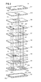
- FIG. 2 is an exploded perspective view of a multilayer band-pass filter 101 according to the first preferred embodiment.
- FIG. 3 is an external perspective view of the multilayer band-pass filter 101 .
- FIG. 4 is an equivalent circuit diagram of the multilayer band-pass filter 101 .
- the multilayer band-pass filter 101 preferably is a band-pass filter that includes an unbalanced terminal UB and balanced terminals B 1 and B 2 and has the balanced-unbalanced transforming function.
- the LC parallel resonator connected to the unbalanced terminal UB is defined as a first-stage LC parallel resonator
- the LC parallel resonator connected to the balanced terminals B 1 and B 2 is defined as a third-stage LC parallel resonator
- the LC parallel resonator between the first-stage and third-stage LC parallel resonators is defined as a second-stage LC parallel resonator.
- the first-stage LC parallel resonator includes an inductor L 1 and capacitors C 11 and C 12 .
- the second-stage LC parallel resonator includes an inductor L 2 and a capacitor C 20
- the third-stage LC parallel resonator includes an inductor L 3 and capacitors C 31 and C 32 .
- the first-stage LC parallel resonator and the second-stage LC parallel resonator are coupled together, and the second-stage LC parallel resonator and the third-stage LC parallel resonator are coupled together.
- the multilayer band-pass filter 101 preferably is a laminate of a plurality of dielectric layers D 1 to D 11 .
- a ground electrode GND is disposed on the upper surface of the dielectric layer D 1 .
- a first capacitor electrode P 11 and a second capacitor electrode P 12 of the first-stage LC parallel resonator and a first capacitor electrode P 31 and a second capacitor electrode P 32 of the third-stage LC parallel resonator are disposed on the upper surface of the dielectric layer D 2 .
- Jump-coupling capacitor electrodes P 131 and P 132 are disposed on the upper surface of the dielectric layer D 3 .
- An inductor electrode S 1 to provide matching at the unbalanced side is disposed on the upper surface of the dielectric layer D 4 .
- Line electrodes S 22 and S 21 of the second-stage LC parallel resonator are disposed on the upper surfaces of the dielectric layers D 5 and D 6 , respectively.
- Line electrodes S 11 and S 12 of the first-stage LC parallel resonator are disposed on the upper surfaces of the dielectric layers D 7 and D 8 , respectively.
- line electrodes S 31 and S 32 of the third-stage LC parallel resonator are disposed on the upper surfaces of the dielectric layers D 7 and D 8 , respectively.
- a first capacitor electrode P 21 and a second capacitor electrode P 22 of the second-stage LC parallel resonator are disposed on the upper surfaces of the dielectric layers D 9 and D 10 , respectively.
- Via electrodes V 11 , V 12 , V 31 , and V 32 extend along the direction in which the dielectric layers D 3 to D 8 are laminated.
- a via electrode V 21 extends along the direction in which the dielectric layers D 6 to D 9 are laminated.
- a via electrode V 22 extends along the direction in which the dielectric layers D 6 to D 10 are laminated.
- the via electrode V 11 extends from a first end of the line electrode S 12 to the capacitor electrode P 11 .
- the via electrode V 12 extends from a second end of the line electrode S 12 to the capacitor electrode P 12 .
- the line electrode S 11 is on a layer adjacent to the line electrode S 12 and is connected to the line electrode S 12 substantially in parallel therewith through the via electrodes V 11 and V 12 disposed therebetween.
- the inductor electrode of the first-stage LC parallel resonator is configured in a loop shape by including the via electrodes V 11 and V 12 and the line electrodes S 11 and S 12 .
- the via electrode V 21 extends from a first end of the line electrode S 22 to the capacitor electrode P 21 .
- the via electrode V 22 extends from a second end of the line electrode S 22 to the capacitor electrode P 22 .
- the line electrode S 21 is on a layer adjacent to the line electrode S 22 and is connected to the line electrode S 22 substantially in parallel therewith through the via electrodes V 21 and V 22 disposed therebetween.
- the inductor electrode of the second-stage LC parallel resonator is configured in a loop shape by including the via electrodes V 21 and V 22 and the line electrodes S 21 and S 22 .
- the via electrode V 31 extends from a first end of the line electrode S 32 to the capacitor electrode P 31 .
- the via electrode V 32 extends from a second end of the line electrode S 32 to the capacitor electrode P 32 .
- the line electrode S 31 is on a layer adjacent to the line electrode S 32 and is connected to the line electrode S 32 substantially in parallel therewith through the via electrodes V 31 and V 32 disposed therebetween.
- the inductor electrode of the third-stage LC parallel resonator is configured in a loop shape by including the via electrodes V 31 and V 32 and the line electrodes S 31 and S 32 .
- a laminate of a plurality of dielectric layers and a plurality of electrode layers is formed by lamination of a plurality of dielectric layers having various types of electrode layer patterns.
- the first-stage LC parallel resonator corresponds to “first first-type LC parallel resonator” in the claims
- the third-stage LC parallel resonator corresponds to “second first-type LC parallel resonator” in the claims.
- the first-stage LC parallel resonator and the third-stage LC parallel resonator are not adjacent to each other on an equivalent circuit.
- the second-stage LC parallel resonator corresponds to “second-type LC parallel resonator” in the claims.
- the direction in which the via electrodes V 11 and V 12 connecting the capacitor electrodes P 11 and P 12 and the line electrodes S 11 and S 12 of the first-stage LC parallel resonator extend from the capacitor electrodes P 11 and P 12 is opposite to the direction in which the via electrodes V 21 and V 22 connecting the capacitor electrodes P 21 and P 22 and the line electrodes S 21 and S 22 of the second-stage LC parallel resonator extend from the capacitor electrodes P 21 and P 22 .
- the direction in which the via electrodes V 31 and V 32 connecting the capacitor electrodes P 31 and P 32 and the line electrodes S 31 and S 32 of the third-stage LC parallel resonator extend from the capacitor electrodes P 31 and P 32 is opposite to the direction in which the via electrodes V 21 and V 22 connecting the capacitor electrodes P 21 and P 22 and the line electrodes S 21 and S 22 of the second-stage LC parallel resonator extend from the capacitor electrodes P 21 and P 22 .
- the jump-coupling capacitor electrodes P 131 and P 132 that generates jump-coupling capacitance between the first-stage and third-stage LC parallel resonators are distant in the lamination direction from the capacitor electrodes P 21 and P 22 of the second-stage LC parallel resonator, which is not related to the jump-coupling. Therefore, virtually no unnecessary stray capacitance occurs between the capacitor electrodes of the second-stage LC parallel resonator and the jump-coupling capacitor electrodes.
- the multilayer band-pass filter 101 includes input and output terminals on four side surfaces (end surfaces) of the laminate.
- the input and output terminals include ground terminals G 1 , G 2 , and G 3 , the unbalanced terminal UB, the balanced terminals B 1 and B 2 , and vacant terminals NC 1 and NC 2 .
- the ground terminals G 1 , G 2 , and G 3 are electrically connected to lead electrodes EG 1 , EG 2 , and EG 3 illustrated in FIG. 2 , respectively.
- the unbalanced terminal UB is electrically connected to a lead electrode EU.
- the balanced terminals B 1 and B 2 are electrically connected to lead electrodes EB 1 and EB 2 , respectively.
- each layer is low temperature co-fired ceramic (LTCC) having a dielectric constant in a range of from 6 to 80.
- Dielectric layers laminated on the electrode layers including the above-described line electrodes have a relative dielectric constant in a range of from 6 to 80.
- Dielectric layers on which the capacitor electrodes are disposed have a relative dielectric constant equal to or more than 20.
- Each of the dielectric layers can be made using low temperature co-fired ceramic formed from a glass component and at least one component of titanium oxide, barium oxide, alumina, and another material, for example. The above-described materials of each dielectric layer can apply to those in other preferred embodiments described below.
- the inductor L 1 is an inductor including the via electrodes V 11 and V 12 and the line electrodes S 11 and S 12 .
- the inductor L 2 is an inductor including the via electrodes V 21 and V 22 and the line electrodes S 21 and S 22 .
- the inductor L 3 is an inductor including the via electrodes V 31 and V 32 and the line electrodes S 31 and S 32 .
- An inductor LU is an inductor including the inductor electrode S 1 to perform matching at the unbalanced side.
- the capacitors C 11 and C 12 are capacitors configured between the ground electrode GND and the capacitor electrodes P 11 and P 12 .
- the capacitor C 20 is a capacitor configured between the capacitor electrodes P 21 and P 22 .
- the capacitors C 31 and C 32 are capacitors configured between the ground electrode GND and the capacitor electrodes P 31 and P 32 .
- a capacitor C 131 is a capacitor configured between the jump-coupling capacitor electrode P 131 and the capacitor electrodes P 11 and P 31 .
- a capacitor C 132 is a capacitor configured between the jump-coupling capacitor electrode P 132 and the capacitor electrodes P 12 and P 32 .
- inductor L 1 and the capacitors C 11 and C 12 define the first-stage LC parallel resonator.
- the inductor L 2 and the capacitor C 20 define the second-stage LC parallel resonator, and the inductor L 3 and the capacitors C 31 and C 32 define the third-stage LC parallel resonator.
- inductive coupling occurs between the inductor electrodes of adjacent LC parallel resonators. Because the inductor electrodes of the adjacent LC parallel resonators are near each other, capacitive coupling (electric-field coupling) occurs therebetween. A positional relationship of the inductor and the capacitors of the first-stage LC parallel resonator is opposite to that of the second-stage LC parallel resonator.
- capacitive coupling between the first-stage and second-stage LC parallel resonators is larger than inductive coupling therebetween, and thus the first-stage and second-stage LC parallel resonators are capacitively coupled.
- a positional relationship of the inductor and the capacitors of the second-stage LC parallel resonator is opposite to that of the third-stage LC parallel resonator.
- the second-stage and third-stage LC parallel resonators are capacitively coupled.
- the capacitors C 131 and C 132 illustrated in FIG. 4 enable the first-stage and third-stage LC parallel resonators to be capacitively jump-coupled to each other.
- FIGS. 5A and 5B illustrate example characteristics of the multilayer band-pass filter 101 according to the first preferred embodiment and a comparative multilayer band-pass filter.
- FIG. 5A illustrates band-pass characteristics (s-parameter S 21 characteristic) of the multilayer band-pass filters.
- FIG. 5B illustrates characteristics of a phase difference between the balanced terminals B 1 and B 2 .
- a curve ⁇ represents characteristics of the multilayer band-pass filter according to the first preferred embodiment
- a curve ⁇ represents characteristics of the comparative multilayer band-pass filter.
- the first-stage, second-stage, and third-stage LC parallel resonators have substantially the same positional relationship between the capacitor electrodes and the inductor electrode in FIG. 2 .
- the via electrodes connecting the capacitor electrodes and the line electrodes in the three LC parallel resonators extend in substantially the same direction from the capacitor electrodes.
- an attenuation pole P 1 results from jump-coupling between the first-stage and third-stage LC parallel resonators.
- An attenuation pole P 2 results from coupling between the first-stage and second-stage LC parallel resonators and coupling between the second-stage and third-stage LC parallel resonators (each coupling being coupling between LC parallel resonators having opposite directions).
- the attenuations at the attenuation poles P 1 and P 2 of the curve ⁇ are larger than those of the curve ⁇ . Because a positional relationship of the capacitor electrodes and the inductor electrode of the second-stage LC parallel resonator is opposite to that of each of the first-stage and third-stage LC parallel resonators, coupling between the second-stage LC parallel resonator and each of the first-stage and third-stage LC parallel resonators can be capacitive coupling. This enables a multilayer band-pass filter that has a narrow pass band to be provided. Additionally, this results in a reduction in insertion loss of the multilayer band-pass filter.
- the phase difference between the balanced terminals of the multilayer band-pass filter according to the first preferred embodiment is closer to 180 degrees than that of the traditional multilayer band-pass filter. Accordingly, the balance characteristics of the filter are improved.
- FIG. 6 is an exploded perspective view of a multilayer band-pass filter 102 according to a second preferred embodiment of the present invention.
- FIG. 7 is an equivalent circuit diagram of the multilayer band-pass filter 102 .
- the multilayer band-pass filter 101 according to the first preferred embodiment of the present invention includes three LC parallel resonators, whereas the multilayer band-pass filter 102 according to the second preferred embodiment of the present invention includes four LC parallel resonators.
- the line electrodes S 32 and S 31 of the third-stage LC parallel resonator are disposed on the upper surfaces of the dielectric layers D 5 and D 6 , respectively.
- the LC parallel resonator connected to an unbalanced terminal is defined as a first-stage LC parallel resonator
- the LC parallel resonator connected to the balanced terminals is defined as a fourth-stage LC parallel resonator.
- the LC parallel resonator coupled to the first-stage LC parallel resonator is defined as a second-stage LC parallel resonator
- the LC parallel resonator coupled to the fourth-stage LC parallel resonator is defined as a third-stage LC parallel resonator.
- the capacitor electrodes P 31 and P 32 of the third-stage LC parallel resonator are disposed on the upper surfaces of the dielectric layers D 9 and D 10 , respectively.
- the via electrode V 31 extends along the direction in which the dielectric layers D 6 to D 9 are laminated.
- the via electrode V 32 extends along the direction in which the dielectric layers D 6 to D 10 are laminated.
- Line electrodes S 41 and S 42 of the fourth-stage LC parallel resonator are disposed on the upper surfaces of the dielectric layers D 7 and D 8 , respectively.
- Capacitor electrodes P 41 and P 42 of the fourth-stage LC parallel resonator are disposed on the upper surface of the dielectric layer D 2 .
- Via electrodes V 41 and V 42 extend along the direction in which the dielectric layers D 3 to D 8 are laminated.
- the line electrode S 41 is on a layer adjacent to the line electrode S 42 and is connected to the line electrode S 42 substantially in parallel therewith through the via electrodes V 41 and V 42 disposed therebetween.
- Jump-coupling capacitor electrodes P 141 and P 142 are disposed on the upper surface of the dielectric layer D 3 .
- the other configuration is substantially the same as in the multilayer band-pass filter 101 according to the first preferred embodiment.
- the first-stage LC parallel resonator corresponds to “first first-type LC parallel resonator” in the claims
- the fourth-stage LC parallel resonator corresponds to “second first-type LC parallel resonator” in the claims.
- the first-stage LC parallel resonator and the fourth-stage LC parallel resonator are not adjacent to each other on an equivalent circuit.
- the second-stage and third-stage LC parallel resonators correspond to “second-type LC parallel resonator” in the claims.
- the direction in which the via electrodes connecting the capacitor electrodes and the line electrodes of the first-type LC parallel resonators extend from the capacitor electrodes is opposite to the direction in which the via electrodes connecting the capacitor electrodes and the line electrodes of the second-type LC parallel resonator extend from the capacitor electrodes.
- the jump-coupling capacitor electrodes P 141 and P 142 forming jump-coupling capacitance between the first-stage and fourth-stage LC parallel resonators are distant in the lamination direction from the capacitor electrodes P 21 and P 22 of the second-stage LC parallel resonator, which is not related to this jump-coupling. Therefore, virtually no unnecessary stray capacitance occurs between the capacitor electrodes of the second-stage and third-stage LC parallel resonators and the jump-coupling capacitor electrodes.
- FIG. 7 is an equivalent circuit diagram of the multilayer band-pass filter 102 according to the second preferred embodiment of the present invention.
- the inductor L 3 is an inductor including the via electrodes V 31 and V 32 and the line electrodes S 31 and S 32 .
- An inductor L 4 is an inductor including the via electrodes V 41 and V 42 and the line electrodes S 41 and S 42 .
- a capacitor C 30 is a capacitor configured between the capacitor electrodes P 31 and P 32 .
- Capacitors C 41 and C 42 are capacitors configured between the ground electrode GND and the capacitor electrodes P 41 and P 42 .
- a capacitor C 141 is a capacitor configured between the jump-coupling capacitor electrode P 141 and the capacitor electrodes P 11 and P 41 .
- a capacitor C 142 is a capacitor configured between the jump-coupling capacitor electrode P 142 and the capacitor electrodes P 12 and P 42 .
- the other configuration is substantially the same as in the multilayer band-pass filter according to the first preferred embodiment of the present invention.
- the multilayer band-pass filter including the four LC parallel resonators described above can also achieve a configuration that has virtually no unnecessary parasitic capacitance occurring between a jump-coupling capacitor and a capacitor electrode of an LC parallel resonator that is not related to the jump-coupling.
- FIG. 8 is an exploded perspective view of a multilayer band-pass filter 103 according to a third preferred embodiment of the present invention.
- the multilayer band-pass filter 103 is different from the multilayer band-pass filter according to the first preferred embodiment of the present invention in that it includes a matching circuit at the balanced side.
- Inductor electrodes S 33 and S 34 to perform matching at the balanced side are disposed on the upper surface of a dielectric layer D 12 .
- First ends of the inductor electrodes S 33 and S 34 to perform matching at the balanced side are electrically connected to the lead electrodes EB 1 and EB 2 , respectively, and second ends thereof are electrically connected to the via electrodes V 31 and V 32 , respectively.
- a capacitor electrode P 33 is disposed on the upper surface of the dielectric layer D 3 .
- the capacitor electrode P 33 is opposed to the inductor electrodes S 33 and S 34 to perform matching at the balanced side and is arranged so as to extend across the gap therebetween.
- the other configuration is substantially the same as in the multilayer band-pass filter illustrated in the first preferred embodiment of the present invention.
- FIG. 9 is an equivalent circuit diagram of the multilayer band-pass filter 103 according to the third preferred embodiment of the present invention.
- inductors LB 1 and LB 2 are inductors including the inductor electrodes S 33 and S 34 to perform matching at the balanced side.
- Capacitors CB 1 and CB 2 are the ones by which capacitance occurring between the capacitor electrode P 33 and each of the capacitor electrodes P 31 and P 32 is symbolized.
- the capacitor CB 1 and the capacitor CB 2 preferably have the same or substantially the same capacitance. Capacitance occurring between the capacitor electrode P 33 and each of the inductor electrodes S 33 and S 34 to perform matching at the balanced side is connected between the balanced terminals B 1 and B 2 .
- this can mean that the capacitors CB 1 and CB 2 having capacitance substantially twice that of the above-described capacitor CB 1 or the above-described capacitor CB 2 are connected between the ground and each of the balanced terminals B 1 and B 2 , as illustrated in FIG. 9 .
- the output impedance of each of the balanced terminals B 1 and B 2 is adjustable by a change in a device value of at least one of the inductors LB 1 and LB 2 and the capacitors CB 1 and CB 2 .
- incorporating the matching circuit connected to the balanced terminals in the multilayer band-pass filter can achieve impedance-matching with a circuit connected to the balanced terminals B 1 and B 2 of the multilayer band-pass filter without an external matching circuit. This facilitates connection to a mother board or other substrates.
- the inductor electrodes S 33 and S 34 to perform matching at the balanced side are disposed on the dielectric layer D 12 , which is different from the dielectric layers D 5 to D 10 on which the inductor electrode of the second-stage LC parallel resonator are disposed, the inductor electrodes S 33 and S 34 to perform matching at the balanced side do not affect coupling between the second-stage and third-stage LC parallel resonators.
- FIG. 10 is an exploded perspective view of a three-stage multilayer band-pass filter 104 according to a fourth preferred embodiment of the present invention.
- the LC parallel resonator connected to the unbalanced terminal is defined as a first-stage LC parallel resonator
- the LC parallel resonator connected to the balanced terminals is defined as a third-stage LC parallel resonator
- the LC parallel resonator between the first-stage and third-stage LC parallel resonators is defined as a second-stage LC parallel resonator.
- Ground electrodes GND 1 and GND 2 are disposed on the upper surface of the dielectric layer D 1 .
- the capacitor electrodes P 11 and P 12 of the first-stage LC parallel resonator and the capacitor electrodes P 31 and P 32 of the third-stage LC parallel resonator are disposed on the upper surface of the dielectric layer D 2 .
- the jump-coupling capacitor electrodes P 131 and P 132 are disposed on the upper surface of the dielectric layer D 3 .
- the line electrodes S 22 and S 21 of the second-stage LC parallel resonator are disposed on the upper surfaces of the dielectric layers D 5 and D 6 , respectively.
- the line electrodes S 11 and S 12 of the first-stage LC parallel resonator are disposed on the upper surfaces of the dielectric layers D 7 and D 8 , respectively.
- the line electrodes S 31 and S 32 of the third-stage LC parallel resonator are disposed on the upper surfaces of the dielectric layers D 7 and D 8 , respectively.
- the capacitor electrodes P 21 and P 22 of the second-stage LC parallel resonator are disposed on the upper surfaces of the dielectric layers D 9 and D 10 , respectively.
- the via electrodes V 11 , V 12 , V 31 , and V 32 extend along the direction in which the dielectric layers D 3 , D 7 , and D 8 are laminated.
- the via electrode V 21 extends along the direction in which the dielectric layers D 6 , D 1 , D 2 , D 3 , D 7 , D 8 , and D 9 are laminated.
- the via electrode V 22 extends along the direction in which the dielectric layers D 6 , D 1 , D 2 , D 3 , D 7 , D 8 , D 9 , and D 10 are laminated.
- the via electrode V 11 extends from the first end of the line electrode S 12 to the capacitor electrode P 11 .
- the via electrode V 12 extends from the second end of the line electrode S 12 to the capacitor electrode P 12 .
- the line electrode S 11 is on a layer adjacent to the line electrode S 12 and is connected to the line electrode S 12 substantially in parallel therewith through the via electrodes V 11 and V 12 disposed therebetween.
- the via electrodes V 21 and V 22 and the line electrodes S 21 and S 22 define the second-stage LC parallel resonator.
- the other configuration is substantially the same as in the multilayer band-pass filter illustrated in the first preferred embodiment of the present invention.
- the line electrodes S 21 and S 22 of the second-stage LC parallel resonator which is not related to jump-coupling, may partially overlap the jump-coupling capacitor electrodes P 131 and P 132 and the ground electrodes GND 1 and GND 2 when viewed from a direction substantially perpendicular to the direction in which the dielectric layers are laminated.
- the line electrodes S 21 and S 22 When the line electrodes S 21 and S 22 are viewed in reference to the capacitor electrodes P 21 and P 22 , i.e., when the direction in which the via electrodes V 21 and V 22 extend is viewed from the capacitor electrodes P 21 and P 22 , the line electrodes S 21 and S 22 may be more distant than the capacitor electrodes P 11 , P 12 , P 31 , and P 32 of the other LC parallel resonators (first-stage and third-stage LC parallel resonators) are.
- the proportion of the via electrodes in the inductor components of the second-stage LC parallel resonator is large, the Q value of the band-pass filter can be increased, and lower insertion loss characteristics are obtainable.
- FIG. 11A is an exploded perspective view of a multilayer band-pass filter 105 according to a fifth preferred embodiment
- FIG. 11B is an external perspective view thereof.
- the mounting surface of the multilayer band-pass filter according to the fifth preferred embodiment is substantially parallel with the direction in which the dielectric layers and the electrode layers are laminated.
- the LC parallel resonator connected to the unbalanced terminal is defined as a first-stage LC parallel resonator
- the LC parallel resonator connected to the balanced terminals is defined as a third-stage LC parallel resonator
- the LC parallel resonator between the first-stage and third-stage LC parallel resonators is defined as a second-stage LC parallel resonator.
- the ground electrode GND 1 is disposed on the dielectric layer D 1 .
- the capacitor electrodes P 11 and P 12 of the first-stage LC parallel resonator and the capacitor electrodes P 31 and P 32 of the third-stage LC parallel resonator are disposed on the dielectric layer D 2 .
- the jump-coupling capacitor electrodes P 131 and P 132 are disposed on the dielectric layer D 3 .
- the line electrode S 21 of the second-stage LC parallel resonator is disposed on the upper surface of the dielectric layer D 5 .
- the line electrode S 11 of the first-stage LC parallel resonator and the line electrode S 31 of the third-stage LC parallel resonator are disposed on the dielectric layer D 7 .
- the capacitor electrodes P 21 and P 22 of the second-stage LC parallel resonator are disposed on the dielectric layers D 9 and D 10 , respectively.
- the via electrodes V 11 , V 12 , V 31 , and V 32 extend along the direction in which the dielectric layers D 3 , D 5 , D 4 , and D 7 are laminated.
- the via electrode V 21 extends along the direction in which the dielectric layers D 4 , D 7 , and D 9 are laminated.
- the via electrode V 22 extends along the direction in which the dielectric layers D 4 , D 7 , D 9 , and D 10 are laminated.
- the via electrode V 11 extends from a first end of the line electrode S 11 to the capacitor electrode P 11 .
- the via electrode V 12 extends from a second end of the line electrode S 12 to the capacitor electrode P 12 .
- the via electrode V 31 extends from a first end of the line electrode S 31 to the capacitor electrode P 31 .
- the via electrode V 32 extends from a second end of the line electrode S 31 to the capacitor electrode P 32 .
- the via electrode V 21 extends from a first end of the line electrode S 21 to the capacitor electrode P 21 .
- the via electrode V 22 extends from a second end of the line electrode S 21 to the capacitor electrode P 22 .
- the capacitor electrodes P 11 and P 12 , the via electrodes V 11 and V 12 , and the line electrode S 11 define the first-stage LC parallel resonator.
- the capacitor electrodes P 21 and P 22 , the via electrodes V 21 and V 22 , and the line electrode S 21 define the second-stage LC parallel resonator.
- the capacitor electrodes P 31 and P 32 , the via electrodes V 31 and V 32 , and the line electrode S 31 define the third-stage LC parallel resonator.
- the multilayer band-pass filter 105 includes input and output terminals on two side surfaces (end surfaces) of the laminate.
- the input and output terminals include the ground terminal G 1 , the unbalanced terminal UB, and the balanced terminals B 1 and B 2 .
- the unbalanced terminal UB is electrically connected to the lead electrode EU illustrated in FIG. 11A .
- the balanced terminals B 1 and B 2 are electrically connected to the lead electrodes EB 1 and EB 2 , respectively.
- a ground electrode GND 3 is disposed on the lower surface of the laminate.
- the ground electrode GND 3 is electrically connected to the ground electrode GND 1 on the dielectric layer D 1 .
- a surface on which the ground electrode GND 3 is disposed is its mounting surface.
- the loop surfaces of the plurality of LC parallel resonators may face a ground electrode substantially in parallel therewith.
- all the inductor electrodes of the LC parallel resonators have substantially the same distance between the ground electrode and each of the line electrodes and via electrodes defining the inductor electrodes. Accordingly, the impedance of each inductor can be easily designed, and stable characteristics are obtainable.
- FIG. 12 is an exploded perspective view of a multilayer band-pass filter 106 according to a sixth preferred embodiment of the present invention.
- the ground electrode GND 2 facing the capacitor electrode P 21 is disposed on the dielectric layer D 10 .
- the ground electrode GND 2 is electrically connected to the ground electrode GND 3 being substantially parallel with the mounting surface as shown in FIG. 11B .
- the other configuration is substantially the same as in the multilayer band-pass filter illustrated in the fifth preferred embodiment of the present invention.
- one of the capacitor electrodes of the second-stage LC parallel resonator which is not related to jump-coupling, may be grounded. Surrounding the plurality of LC parallel resonators with the ground electrodes GND 1 , GND 2 , and GND 3 reduces and minimizes the effects of electromagnetic radiation on the multilayer band-pass filter 106 .
Landscapes
- Physics & Mathematics (AREA)
- Electromagnetism (AREA)
- Filters And Equalizers (AREA)
- Control Of Motors That Do Not Use Commutators (AREA)
- Piezo-Electric Or Mechanical Vibrators, Or Delay Or Filter Circuits (AREA)
Abstract
Description
Claims (6)
Applications Claiming Priority (4)
| Application Number | Priority Date | Filing Date | Title |
|---|---|---|---|
| JP2010253214 | 2010-11-11 | ||
| JP2010-253214 | 2010-11-11 | ||
| JP2011151479A JP4883237B1 (en) | 2010-11-11 | 2011-07-08 | Multilayer bandpass filter |
| JP2011-151479 | 2011-07-08 |
Publications (2)
| Publication Number | Publication Date |
|---|---|
| US20120119852A1 US20120119852A1 (en) | 2012-05-17 |
| US8754726B2 true US8754726B2 (en) | 2014-06-17 |
Family
ID=45851250
Family Applications (1)
| Application Number | Title | Priority Date | Filing Date |
|---|---|---|---|
| US13/193,649 Active 2032-05-30 US8754726B2 (en) | 2010-11-11 | 2011-07-29 | Multilayer band-pass filter |
Country Status (4)
| Country | Link |
|---|---|
| US (1) | US8754726B2 (en) |
| JP (1) | JP4883237B1 (en) |
| CN (1) | CN102468814B (en) |
| TW (1) | TWI442622B (en) |
Cited By (8)
| Publication number | Priority date | Publication date | Assignee | Title |
|---|---|---|---|---|
| US20130229241A1 (en) * | 2010-12-06 | 2013-09-05 | Murata Manufacturing Co., Ltd. | Multilayer band pass filter |
| US11071239B2 (en) | 2018-09-18 | 2021-07-20 | Avx Corporation | High power surface mount filter |
| US11114993B2 (en) | 2018-12-20 | 2021-09-07 | Avx Corporation | High frequency multilayer filter |
| US11114994B2 (en) | 2018-12-20 | 2021-09-07 | Avx Corporation | Multilayer filter including a low inductance via assembly |
| US11336249B2 (en) | 2018-12-20 | 2022-05-17 | KYOCERA AVX Components Corporation | Multilayer filter including a capacitor connected with at least two vias |
| US11509276B2 (en) | 2018-12-20 | 2022-11-22 | KYOCERA AVX Components Corporation | Multilayer filter including a return signal reducing protrusion |
| US11563414B2 (en) | 2018-12-20 | 2023-01-24 | KYOCERA AVX Components Corporation | Multilayer electronic device including a capacitor having a precisely controlled capacitive area |
| US11595013B2 (en) | 2018-12-20 | 2023-02-28 | KYOCERA AVX Components Corporation | Multilayer electronic device including a high precision inductor |
Families Citing this family (27)
| Publication number | Priority date | Publication date | Assignee | Title |
|---|---|---|---|---|
| JP5637150B2 (en) * | 2012-01-11 | 2014-12-10 | Tdk株式会社 | Multilayer bandpass filter |
| CN103579731B (en) * | 2012-08-03 | 2018-04-03 | Tdk株式会社 | Lit-par-lit structure type balanced unbalanced transformer |
| US9853620B2 (en) * | 2013-05-03 | 2017-12-26 | Skyworks Solutions, Inc. | Coupled-resonator on-die filters for WiFi applications |
| JP5741783B1 (en) * | 2013-10-24 | 2015-07-01 | 株式会社村田製作所 | Composite LC resonator and bandpass filter |
| JP6354551B2 (en) * | 2014-12-02 | 2018-07-11 | 株式会社村田製作所 | Electronic components |
| JP6504021B2 (en) * | 2015-11-04 | 2019-04-24 | 株式会社村田製作所 | Electronic parts |
| WO2018100923A1 (en) * | 2016-12-02 | 2018-06-07 | 株式会社村田製作所 | Lc resonator and lc filter |
| JP6791107B2 (en) * | 2017-12-08 | 2020-11-25 | 株式会社村田製作所 | Stacked band pass filter |
| WO2019146441A1 (en) | 2018-01-26 | 2019-08-01 | 株式会社村田製作所 | Bandpass filter |
| WO2020105257A1 (en) * | 2018-11-22 | 2020-05-28 | 株式会社村田製作所 | Resonant element, filter, and diplexer |
| WO2020148683A1 (en) * | 2019-01-15 | 2020-07-23 | Telefonaktiebolaget Lm Ericsson (Publ) | Miniature filter design for antenna systems |
| JP7232083B2 (en) * | 2019-03-05 | 2023-03-02 | 太陽誘電株式会社 | filter |
| WO2021005927A1 (en) * | 2019-07-09 | 2021-01-14 | 株式会社村田製作所 | Lc filter |
| WO2021029154A1 (en) * | 2019-08-10 | 2021-02-18 | 株式会社村田製作所 | Diplexer |
| CN114208030B (en) * | 2019-12-03 | 2025-12-12 | 株式会社村田制作所 | Stacked filters |
| CN115298957B (en) * | 2020-04-10 | 2025-10-31 | 株式会社村田制作所 | LC resonator and LC filter |
| CN115461931B (en) * | 2020-05-25 | 2024-06-04 | 株式会社村田制作所 | LC filter, and duplexer and multiplexer using the same |
| CN115917965B (en) * | 2020-07-01 | 2025-10-28 | 株式会社村田制作所 | Filter device and multiplexer |
| WO2022065201A1 (en) * | 2020-09-28 | 2022-03-31 | 株式会社村田製作所 | Filter device and high-frequency front end circuit provided therewith |
| WO2022070739A1 (en) * | 2020-09-29 | 2022-04-07 | 株式会社村田製作所 | Resonant element, filter, and module |
| JP7622814B2 (en) * | 2021-02-26 | 2025-01-28 | 株式会社村田製作所 | Multilayer LC Filter |
| JP7663462B2 (en) * | 2021-09-14 | 2025-04-16 | Tdk株式会社 | Multilayer Electronic Components |
| JP7709361B2 (en) * | 2021-10-26 | 2025-07-16 | Tdk株式会社 | Multilayer filter device |
| CN114285387B (en) * | 2021-12-09 | 2023-05-09 | 电子科技大学 | A kind of small LC filter and its preparation method |
| JP2023113307A (en) * | 2022-02-03 | 2023-08-16 | Tdk株式会社 | Filter circuit and stacked filter device |
| JP2024021356A (en) * | 2022-08-03 | 2024-02-16 | Tdk株式会社 | laminated filter |
| CN116960587A (en) * | 2023-07-13 | 2023-10-27 | 环旭电子股份有限公司 | Filter and circuit element |
Citations (5)
| Publication number | Priority date | Publication date | Assignee | Title |
|---|---|---|---|---|
| JP2006067221A (en) | 2004-08-26 | 2006-03-09 | Ngk Spark Plug Co Ltd | Multilayer dielectric filter |
| US7126444B2 (en) * | 2003-09-04 | 2006-10-24 | Tdk Corporation | Multi-layer band-pass filter |
| WO2007119356A1 (en) | 2006-04-14 | 2007-10-25 | Murata Manufacturing Co., Ltd. | Layered band pass filter |
| US7432786B2 (en) * | 2006-01-31 | 2008-10-07 | Tdk Corporation | High frequency filter |
| US8482365B2 (en) * | 2008-05-23 | 2013-07-09 | Murata Manufacturing Co., Ltd. | Multilayer bandpass filter |
Family Cites Families (4)
| Publication number | Priority date | Publication date | Assignee | Title |
|---|---|---|---|---|
| JP3084037B2 (en) * | 1990-03-23 | 2000-09-04 | 東光株式会社 | Multilayer resonator and filter using it |
| TW200908430A (en) * | 2007-05-18 | 2009-02-16 | Murata Manufacturing Co | Stacked bandpass filter |
| TW200917563A (en) * | 2007-09-27 | 2009-04-16 | Murata Manufacturing Co | Laminated bandpass filter |
| CN103095245B (en) * | 2008-01-17 | 2016-09-28 | 株式会社村田制作所 | Lamination-type resonator and Mehrschichtiges filter |
-
2011
- 2011-03-31 TW TW100111220A patent/TWI442622B/en active
- 2011-05-23 CN CN201110150315.0A patent/CN102468814B/en active Active
- 2011-07-08 JP JP2011151479A patent/JP4883237B1/en active Active
- 2011-07-29 US US13/193,649 patent/US8754726B2/en active Active
Patent Citations (6)
| Publication number | Priority date | Publication date | Assignee | Title |
|---|---|---|---|---|
| US7126444B2 (en) * | 2003-09-04 | 2006-10-24 | Tdk Corporation | Multi-layer band-pass filter |
| JP2006067221A (en) | 2004-08-26 | 2006-03-09 | Ngk Spark Plug Co Ltd | Multilayer dielectric filter |
| US7432786B2 (en) * | 2006-01-31 | 2008-10-07 | Tdk Corporation | High frequency filter |
| WO2007119356A1 (en) | 2006-04-14 | 2007-10-25 | Murata Manufacturing Co., Ltd. | Layered band pass filter |
| EP2009787A1 (en) | 2006-04-14 | 2008-12-31 | Murata Manufacturing Co. Ltd. | Layered band pass filter |
| US8482365B2 (en) * | 2008-05-23 | 2013-07-09 | Murata Manufacturing Co., Ltd. | Multilayer bandpass filter |
Cited By (11)
| Publication number | Priority date | Publication date | Assignee | Title |
|---|---|---|---|---|
| US20130229241A1 (en) * | 2010-12-06 | 2013-09-05 | Murata Manufacturing Co., Ltd. | Multilayer band pass filter |
| US9035724B2 (en) * | 2010-12-06 | 2015-05-19 | Murata Manufacturing Co., Ltd. | Multilayer band pass filter |
| US11071239B2 (en) | 2018-09-18 | 2021-07-20 | Avx Corporation | High power surface mount filter |
| US12058845B2 (en) | 2018-09-18 | 2024-08-06 | KYOCERA AVX Components Corporation | High power surface mount filter |
| US11114993B2 (en) | 2018-12-20 | 2021-09-07 | Avx Corporation | High frequency multilayer filter |
| US11114994B2 (en) | 2018-12-20 | 2021-09-07 | Avx Corporation | Multilayer filter including a low inductance via assembly |
| US11336249B2 (en) | 2018-12-20 | 2022-05-17 | KYOCERA AVX Components Corporation | Multilayer filter including a capacitor connected with at least two vias |
| US11509276B2 (en) | 2018-12-20 | 2022-11-22 | KYOCERA AVX Components Corporation | Multilayer filter including a return signal reducing protrusion |
| US11563414B2 (en) | 2018-12-20 | 2023-01-24 | KYOCERA AVX Components Corporation | Multilayer electronic device including a capacitor having a precisely controlled capacitive area |
| US11595013B2 (en) | 2018-12-20 | 2023-02-28 | KYOCERA AVX Components Corporation | Multilayer electronic device including a high precision inductor |
| US11838002B2 (en) | 2018-12-20 | 2023-12-05 | KYOCERA AVX Components Corporation | High frequency multilayer filter |
Also Published As
| Publication number | Publication date |
|---|---|
| JP4883237B1 (en) | 2012-02-22 |
| CN102468814A (en) | 2012-05-23 |
| CN102468814B (en) | 2014-10-01 |
| TWI442622B (en) | 2014-06-21 |
| TW201220592A (en) | 2012-05-16 |
| JP2012120149A (en) | 2012-06-21 |
| US20120119852A1 (en) | 2012-05-17 |
Similar Documents
| Publication | Publication Date | Title |
|---|---|---|
| US8754726B2 (en) | Multilayer band-pass filter | |
| US8760242B2 (en) | Multilayer bandpass filter | |
| US7907034B2 (en) | Laminated band-pass filter having an even number of LC parallel resonators | |
| CN102132490B (en) | Laminated balance filter | |
| US9035724B2 (en) | Multilayer band pass filter | |
| US9473103B2 (en) | High frequency component | |
| CN101421918B (en) | Layered band-pass filter | |
| US8482366B2 (en) | Laminated balance filter | |
| US8212633B2 (en) | Laminated band pass filter | |
| US8975983B2 (en) | Band-pass filter | |
| US7432786B2 (en) | High frequency filter | |
| US9306528B2 (en) | Composite LC resonator and band pass filter | |
| US8629736B2 (en) | Directional coupler | |
| WO2009142113A1 (en) | Layered bandpass filter | |
| WO2013069498A1 (en) | Lc filter circuit and high-frequency module | |
| US8098117B2 (en) | LC composite component | |
| US8018305B2 (en) | Electronic component | |
| WO2015059963A1 (en) | Composite lc resonator and bandpass filter | |
| JP4197032B2 (en) | Two-port nonreciprocal circuit device and communication device |
Legal Events
| Date | Code | Title | Description |
|---|---|---|---|
| AS | Assignment |
Owner name: MURATA MANUFACTURING CO., LTD., JAPAN Free format text: ASSIGNMENT OF ASSIGNORS INTEREST;ASSIGNORS:SASAKI, HIROYUKI;MASUDA, HIROSHI;TANIGUCHI, TETSUO;REEL/FRAME:026671/0136 Effective date: 20110720 |
|
| FEPP | Fee payment procedure |
Free format text: PAYOR NUMBER ASSIGNED (ORIGINAL EVENT CODE: ASPN); ENTITY STATUS OF PATENT OWNER: LARGE ENTITY |
|
| STCF | Information on status: patent grant |
Free format text: PATENTED CASE |
|
| FEPP | Fee payment procedure |
Free format text: PAYER NUMBER DE-ASSIGNED (ORIGINAL EVENT CODE: RMPN); ENTITY STATUS OF PATENT OWNER: LARGE ENTITY Free format text: PAYOR NUMBER ASSIGNED (ORIGINAL EVENT CODE: ASPN); ENTITY STATUS OF PATENT OWNER: LARGE ENTITY |
|
| MAFP | Maintenance fee payment |
Free format text: PAYMENT OF MAINTENANCE FEE, 4TH YEAR, LARGE ENTITY (ORIGINAL EVENT CODE: M1551) Year of fee payment: 4 |
|
| MAFP | Maintenance fee payment |
Free format text: PAYMENT OF MAINTENANCE FEE, 8TH YEAR, LARGE ENTITY (ORIGINAL EVENT CODE: M1552); ENTITY STATUS OF PATENT OWNER: LARGE ENTITY Year of fee payment: 8 |
|
| MAFP | Maintenance fee payment |
Free format text: PAYMENT OF MAINTENANCE FEE, 12TH YEAR, LARGE ENTITY (ORIGINAL EVENT CODE: M1553); ENTITY STATUS OF PATENT OWNER: LARGE ENTITY Year of fee payment: 12 |