US8753799B2 - Method for fabricating LCD - Google Patents

Method for fabricating LCD Download PDF

Info

Publication number
US8753799B2
US8753799B2 US13/375,227 US201113375227A US8753799B2 US 8753799 B2 US8753799 B2 US 8753799B2 US 201113375227 A US201113375227 A US 201113375227A US 8753799 B2 US8753799 B2 US 8753799B2
Authority
US
United States
Prior art keywords
mav
organic monomers
glass substrate
fabricating
patterned
Prior art date
Legal status (The legal status is an assumption and is not a legal conclusion. Google has not performed a legal analysis and makes no representation as to the accuracy of the status listed.)
Active, expires
Application number
US13/375,227
Other versions
US20130095430A1 (en
Inventor
Jun Wang
Current Assignee (The listed assignees may be inaccurate. Google has not performed a legal analysis and makes no representation or warranty as to the accuracy of the list.)
TCL China Star Optoelectronics Technology Co Ltd
Original Assignee
Shenzhen China Star Optoelectronics Technology Co Ltd
Priority date (The priority date is an assumption and is not a legal conclusion. Google has not performed a legal analysis and makes no representation as to the accuracy of the date listed.)
Filing date
Publication date
Application filed by Shenzhen China Star Optoelectronics Technology Co Ltd filed Critical Shenzhen China Star Optoelectronics Technology Co Ltd
Assigned to SHENZHEN CHINA STAR OPTOELECTRONICS TECHNOLOGY CO., LTD. reassignment SHENZHEN CHINA STAR OPTOELECTRONICS TECHNOLOGY CO., LTD. ASSIGNMENT OF ASSIGNORS INTEREST (SEE DOCUMENT FOR DETAILS). Assignors: WANG, JUN
Publication of US20130095430A1 publication Critical patent/US20130095430A1/en
Application granted granted Critical
Publication of US8753799B2 publication Critical patent/US8753799B2/en
Active legal-status Critical Current
Adjusted expiration legal-status Critical

Links

Images

Classifications

    • GPHYSICS
    • G02OPTICS
    • G02FOPTICAL DEVICES OR ARRANGEMENTS FOR THE CONTROL OF LIGHT BY MODIFICATION OF THE OPTICAL PROPERTIES OF THE MEDIA OF THE ELEMENTS INVOLVED THEREIN; NON-LINEAR OPTICS; FREQUENCY-CHANGING OF LIGHT; OPTICAL LOGIC ELEMENTS; OPTICAL ANALOGUE/DIGITAL CONVERTERS
    • G02F1/00Devices or arrangements for the control of the intensity, colour, phase, polarisation or direction of light arriving from an independent light source, e.g. switching, gating or modulating; Non-linear optics
    • G02F1/01Devices or arrangements for the control of the intensity, colour, phase, polarisation or direction of light arriving from an independent light source, e.g. switching, gating or modulating; Non-linear optics for the control of the intensity, phase, polarisation or colour 
    • G02F1/13Devices or arrangements for the control of the intensity, colour, phase, polarisation or direction of light arriving from an independent light source, e.g. switching, gating or modulating; Non-linear optics for the control of the intensity, phase, polarisation or colour  based on liquid crystals, e.g. single liquid crystal display cells
    • G02F1/133Constructional arrangements; Operation of liquid crystal cells; Circuit arrangements
    • G02F1/1333Constructional arrangements; Manufacturing methods
    • G02F1/1337Surface-induced orientation of the liquid crystal molecules, e.g. by alignment layers
    • G02F1/133707Structures for producing distorted electric fields, e.g. bumps, protrusions, recesses, slits in pixel electrodes
    • GPHYSICS
    • G02OPTICS
    • G02FOPTICAL DEVICES OR ARRANGEMENTS FOR THE CONTROL OF LIGHT BY MODIFICATION OF THE OPTICAL PROPERTIES OF THE MEDIA OF THE ELEMENTS INVOLVED THEREIN; NON-LINEAR OPTICS; FREQUENCY-CHANGING OF LIGHT; OPTICAL LOGIC ELEMENTS; OPTICAL ANALOGUE/DIGITAL CONVERTERS
    • G02F1/00Devices or arrangements for the control of the intensity, colour, phase, polarisation or direction of light arriving from an independent light source, e.g. switching, gating or modulating; Non-linear optics
    • G02F1/01Devices or arrangements for the control of the intensity, colour, phase, polarisation or direction of light arriving from an independent light source, e.g. switching, gating or modulating; Non-linear optics for the control of the intensity, phase, polarisation or colour 
    • G02F1/13Devices or arrangements for the control of the intensity, colour, phase, polarisation or direction of light arriving from an independent light source, e.g. switching, gating or modulating; Non-linear optics for the control of the intensity, phase, polarisation or colour  based on liquid crystals, e.g. single liquid crystal display cells
    • G02F1/133Constructional arrangements; Operation of liquid crystal cells; Circuit arrangements
    • G02F1/1333Constructional arrangements; Manufacturing methods
    • G02F1/1347Arrangement of liquid crystal layers or cells in which the final condition of one light beam is achieved by the addition of the effects of two or more layers or cells
    • G02F1/13471Arrangement of liquid crystal layers or cells in which the final condition of one light beam is achieved by the addition of the effects of two or more layers or cells in which all the liquid crystal cells or layers remain transparent, e.g. FLC, ECB, DAP, HAN, TN, STN, SBE-LC cells
    • GPHYSICS
    • G02OPTICS
    • G02FOPTICAL DEVICES OR ARRANGEMENTS FOR THE CONTROL OF LIGHT BY MODIFICATION OF THE OPTICAL PROPERTIES OF THE MEDIA OF THE ELEMENTS INVOLVED THEREIN; NON-LINEAR OPTICS; FREQUENCY-CHANGING OF LIGHT; OPTICAL LOGIC ELEMENTS; OPTICAL ANALOGUE/DIGITAL CONVERTERS
    • G02F1/00Devices or arrangements for the control of the intensity, colour, phase, polarisation or direction of light arriving from an independent light source, e.g. switching, gating or modulating; Non-linear optics
    • G02F1/01Devices or arrangements for the control of the intensity, colour, phase, polarisation or direction of light arriving from an independent light source, e.g. switching, gating or modulating; Non-linear optics for the control of the intensity, phase, polarisation or colour 
    • G02F1/13Devices or arrangements for the control of the intensity, colour, phase, polarisation or direction of light arriving from an independent light source, e.g. switching, gating or modulating; Non-linear optics for the control of the intensity, phase, polarisation or colour  based on liquid crystals, e.g. single liquid crystal display cells
    • G02F1/137Devices or arrangements for the control of the intensity, colour, phase, polarisation or direction of light arriving from an independent light source, e.g. switching, gating or modulating; Non-linear optics for the control of the intensity, phase, polarisation or colour  based on liquid crystals, e.g. single liquid crystal display cells characterised by the electro-optical or magneto-optical effect, e.g. field-induced phase transition, orientation effect, guest-host interaction or dynamic scattering
    • G02F1/139Devices or arrangements for the control of the intensity, colour, phase, polarisation or direction of light arriving from an independent light source, e.g. switching, gating or modulating; Non-linear optics for the control of the intensity, phase, polarisation or colour  based on liquid crystals, e.g. single liquid crystal display cells characterised by the electro-optical or magneto-optical effect, e.g. field-induced phase transition, orientation effect, guest-host interaction or dynamic scattering based on orientation effects in which the liquid crystal remains transparent
    • G02F1/1393Devices or arrangements for the control of the intensity, colour, phase, polarisation or direction of light arriving from an independent light source, e.g. switching, gating or modulating; Non-linear optics for the control of the intensity, phase, polarisation or colour  based on liquid crystals, e.g. single liquid crystal display cells characterised by the electro-optical or magneto-optical effect, e.g. field-induced phase transition, orientation effect, guest-host interaction or dynamic scattering based on orientation effects in which the liquid crystal remains transparent the birefringence of the liquid crystal being electrically controlled, e.g. ECB-, DAP-, HAN-, PI-LC cells

Definitions

  • the present invention relates to a liquid crystal display (LCD) technology, and especially to a method for fabricating an LCD by using a photocurable material of a Multi-domain Vertical Alignment (MAV) layer.
  • LCD liquid crystal display
  • MAV Multi-domain Vertical Alignment
  • the LCD In flat panel display devices, the LCD has features of small size, low power consumption, relatively low manufacturing cost and no radiation, and so on, and occupies a dominant position in the current flat panel display market.
  • the MAV technology utilizes protrusions to make liquid-crystal molecules align in a certain angle at rest, unlike a conventional vertical alignment.
  • the liquid-crystal molecules When applying a voltage, the liquid-crystal molecules are twisted to horizontal for making a backlight pass faster, whereby display time can be greatly decreased on the basis of a shorter response time of the vertical alignment of the liquid crystal molecules, a viewing angle thereof is broader, and the viewing angle can be increased to 160 or more degrees.
  • the MAV type LCD has the advantages of a good color performance, a strong pure black performance, wide viewing angle, and so on, so it is abundantly used in the flat panel display industry.
  • the MVA layer In conventional processes of fabricating a MVA layer of the MVA type LCD, the MVA layer usually is formed by the steps of coating, soft baking, exposure, development, hard baking, and so on. There are some problems of complex processes and high technical requirements.
  • An objective of the present invention is to provide a method for fabricating an LCD by using a photocurable material of a MAV layer for solving the complex processes and the high technical requirements.
  • the present invention relates to a method for fabricating an LCD.
  • the method includes fabricating a multi-domain vertical alignment (MAV) layer on a glass substrate.
  • the step of fabricating the MAV layer on the glass substrate comprises the steps of: (A) coating MAV organic monomers on the glass substrate; (B) patterning the MAV organic monomers through a photomask; and (C) curing the patterned MAV organic monomers.
  • the MAV organic monomers has a viscosity of 5 to 500 mPa ⁇ s and a coating thickness of 800 to 1800 nanometers at the step (A).
  • a distance between the photomask and a surface of the MAV organic monomers is 0.3-50 micrometers at the step (B).
  • a light for performing the patterning at the step (B) has a wavelength between 100 to 780 nanometers with an exposure time between 30 to 540 seconds.
  • the method further comprises the steps of: (B1) filtering the MAV organic monomers which are not patterned on the glass substrate; and (B2) cleaning the glass substrate for removing the non-patterned MAV organic monomers remaining in the glass substrate; the step (C) specifically comprises photo-curing and/or heat treating the patterned MAV organic monomers.
  • a wavelength of a light of the photo-curing is between 100 to 780 nanometers with an exposure duration between 30 to 540 seconds.
  • a temperature of the heat treatment is between 50 to 250 degrees with a treatment duration between 30 to 540 seconds.
  • the MAV organic monomers being non-solvent type photocurable organic monomers.
  • the present invention relates to a method for fabricating an LCD.
  • the method includes fabricating a MAV layer on a glass substrate.
  • the step of fabricating the MAV layer on the glass substrate comprises the steps of: (A) coating MAV organic monomers on the glass substrate; (B) patterning the MAV organic monomers through a photomask; and (C) curing the patterned MAV organic monomers.
  • the MAV organic monomers has a viscosity of 5 to 500 mPa ⁇ s and a coating thickness of 800 to 1800 nanometers at the step (A).
  • a distance between the photomask and a surface of the MAV organic monomers are 0.3-50 micrometers at the step (B).
  • a light for performing the patterning at the step (B) has a wavelength between 100 to 780 nanometers with an exposure time between 30 to 540 seconds.
  • the method further comprises the steps of: (B1) filtering the MAV organic monomers which are not patterned on the glass substrate.
  • the method further comprises the step of: (B2) cleaning the glass substrate for removing the non-patterned MVA organic monomers remaining in the glass substrate.
  • the step (C) specifically comprises photo-curing and/or heat treating the patterned MVA organic monomers.
  • a wavelength of a light of the photo-curing is between 100 to 780 nanometers with an exposure duration between 30 to 540 seconds.
  • a temperature of the heat treatment is between 50 to 250 degrees with a treatment duration between 30 to 540 seconds.
  • the MAV organic monomers being non-solvent type photocurable organic monomers.
  • FIG. 1 is a flow chart illustrating a illustrating according to a first preferred embodiment of the present invention
  • FIG. 2 is a flow chart illustrating a illustrating according to a second preferred embodiment of the present invention.
  • FIG. 3 is a flow chart illustrating a illustrating according to a third preferred embodiment of the present invention.
  • FIG. 4 is a first fabricating structural schematic drawing illustrating the method for fabricating an LCD according to the preferred embodiment of the present invention
  • FIG. 5 is a second fabricating structural schematic drawing illustrating the method for fabricating an LCD according to the preferred embodiment of the present invention.
  • FIG. 6 is a third fabricating structural schematic drawing illustrating the method for fabricating an LCD according to the preferred embodiment of the present invention.
  • the present invention relates to a method for fabricating an MAV type LCD.
  • the method includes fabricating a MAV layer on a glass substrate 1 on which a color filter layer and a transparent electrode layer have been formed.
  • Organic monomers for fabricating the MAV layer of the present invention are MVA organic monomers 2 , so the MAV layer of the present invention can be cured directly through the exposure without the soft baking after coating. Therefore, the fabricating processes of the method for fabricating a MAV LCD are simple, environmentally friendly, low-skilled, and the production costs of the LCD can be effectively reduced.
  • the MVA organic monomers 2 herein are MVA organic monomers which can be cured by exposing a light with corresponding wavelengths.
  • FIG. 1 that is a flow chart illustrating a illustrating according to a first preferred embodiment of the present invention, the method for fabricating an LCD begins at step 101 .
  • the MAV organic monomers 2 are coated on the glass substrate 1 .
  • the MAV organic monomers 2 are patterned through a photomask 3 .
  • the MAV organic monomers 2 which have been patterned are cured.
  • FIG. 4 is a first fabricating structural schematic drawing illustrating the method for fabricating an LCD according to the preferred embodiment of the present invention
  • FIG. 5 is a second fabricating structural schematic drawing illustrating the method for fabricating an LCD according to the preferred embodiment of the present invention
  • FIG. 6 is a third fabricating structural schematic drawing illustrating the method for fabricating an LCD according to the preferred embodiment of the present invention.
  • the MVA organic monomers 2 are coated on the glass substrate 1 on which the color filter layer and the transparent electrode layer have been formed.
  • the MAV organic monomers has a viscosity of 5 to 500 mPa ⁇ s and a coating thickness of 800 to 1800 nanometers. Therefore, the MVA organic monomers have a better photo-curing treatment based on the assured thickness of the MVA layer. If the coating thickness is too thick, the MAV layer can not be completely cured finally. If the coating thickness is too thin, the MAV layer can not reach the objective for changing the direction of the liquid-crystal molecules.
  • the photomask 3 with a desired pattern is disposed above the glass substrate 1 coated with the MVA organic monomer 2 , and a distance between the photomask and a surface of the MAV organic monomers are 0.3-50 micrometers. As the distance between the photomask and the surface of the MAV organic monomers are closer, the accuracy of the patterning process is higher. Users can adjust the distance based on the desired accuracy requirement.
  • FIG. 5 illustrates the process that the MVA organic monomers 2 are patterned by using the photomask 3 .
  • a light with a wavelength between 100 to 780 nanometers is utilized to expose the MVA organic monomers 2 via the photomask 3 with an exposure duration between 30 to 540 seconds.
  • the exposure duration can be set according to the various wavelengths and the coating thicknesses of the MVA organic monomers 2 , thereby achieving a best curing effect of the MVA organic monomers.
  • the cured MVA layer is a trapezoid region located on the glass substrate 1 as shown in FIG. 6 .
  • the MAV organic monomers 2 which have been patterned are cured, and the way of the curing is by photo-curing and/or heat treating.
  • a wavelength of a light of the photo-curing is between 100 to 780 nanometers with an exposure duration between 30 to 540 seconds.
  • a temperature of the heat treatment is between 50 to 250 degrees with a treatment duration between 30 to 540 seconds.
  • the users can employ one or two of the above-mentioned curing ways to cure the patterned MVA organic monomers 2 .
  • FIG. 2 that is a flow chart illustrating a illustrating according to a second preferred embodiment of the present invention, the method for fabricating an LCD begins at step 201 .
  • the MAV organic monomers 2 are coated on the glass substrate 1 .
  • the MAV organic monomers 2 are patterned through a photomask 3 .
  • the MAV organic monomers 2 which are not patterned on the glass substrate 1 are filtered.
  • the MAV organic monomers 2 which have been patterned are cured.
  • the filtered MAV organic monomers 2 which are not patterned on the glass substrate 1 can be collected for reusing at next time; thus, the manufacturing costs of LCD can be further reduced.
  • FIG. 3 that is a flow chart illustrating a illustrating according to a third preferred embodiment of the present invention, the method for fabricating an LCD begins at step 301 .
  • the MAV organic monomers 2 are coated on the glass substrate 1 .
  • the MAV organic monomers 2 are patterned through a photomask 3 .
  • the MAV organic monomers 2 which are not patterned on the glass substrate 1 are filtered.
  • the glass substrate 1 is cleaned for removing the non-patterned MVA organic monomers 2 remaining in the glass substrate 1 .
  • the MAV organic monomers 2 which have been patterned are cured.
  • the glass substrate 1 is cleaned by using organic solvents for removing the non-patterned MVA organic monomers 2 remaining in the glass substrate 1 .
  • the MAV organic monomers 2 are non-solvent type photocurable organic monomers. Because the MAV organic monomers 2 are non-solvent type photocurable organic monomers, it can be utilized without dissolving in a solvent, whereby there is no by-product of macromolecules formed during the photo-curing process. Therefore, the curing process is more complete, safe and easier in the curing operation without regarding to the treatment of the by-products.
  • the method for fabricating an LCD of the present invention has the advantages of simple processes, environmental protection, low technical difficulty, and so on, and the manufacturing cost of the LCD can be effectively reduced.

Abstract

The present invention relates to a method for fabricating an LCD. The method includes fabricating a MAV layer on a glass substrate. The step of fabricating the MAV layer on the glass substrate comprises the steps of: (A) coating MAV organic monomers on the glass substrate; (B) patterning the MAV organic monomers through a photomask; and (C) curing the patterned MAV organic monomers. In accordance with a photo-curing material of the MAV layer, the fabricating method of the present invention has simple processes with low technical requirements.

Description

FIELD OF THE INVENTION
The present invention relates to a liquid crystal display (LCD) technology, and especially to a method for fabricating an LCD by using a photocurable material of a Multi-domain Vertical Alignment (MAV) layer.
BACKGROUND OF THE INVENTION
In flat panel display devices, the LCD has features of small size, low power consumption, relatively low manufacturing cost and no radiation, and so on, and occupies a dominant position in the current flat panel display market. The MAV technology utilizes protrusions to make liquid-crystal molecules align in a certain angle at rest, unlike a conventional vertical alignment. When applying a voltage, the liquid-crystal molecules are twisted to horizontal for making a backlight pass faster, whereby display time can be greatly decreased on the basis of a shorter response time of the vertical alignment of the liquid crystal molecules, a viewing angle thereof is broader, and the viewing angle can be increased to 160 or more degrees. Thus, the MAV type LCD has the advantages of a good color performance, a strong pure black performance, wide viewing angle, and so on, so it is abundantly used in the flat panel display industry.
In conventional processes of fabricating a MVA layer of the MVA type LCD, the MVA layer usually is formed by the steps of coating, soft baking, exposure, development, hard baking, and so on. There are some problems of complex processes and high technical requirements.
Therefore, there is a significant need to provide a method for fabricating an LCD for solving the problems existing in the prior art.
SUMMARY OF THE INVENTION
An objective of the present invention is to provide a method for fabricating an LCD by using a photocurable material of a MAV layer for solving the complex processes and the high technical requirements.
To achieve the foregoing objective, the technical solution of this invention is implemented as follows.
The present invention relates to a method for fabricating an LCD. The method includes fabricating a multi-domain vertical alignment (MAV) layer on a glass substrate. The step of fabricating the MAV layer on the glass substrate comprises the steps of: (A) coating MAV organic monomers on the glass substrate; (B) patterning the MAV organic monomers through a photomask; and (C) curing the patterned MAV organic monomers. The MAV organic monomers has a viscosity of 5 to 500 mPa·s and a coating thickness of 800 to 1800 nanometers at the step (A). A distance between the photomask and a surface of the MAV organic monomers is 0.3-50 micrometers at the step (B). A light for performing the patterning at the step (B) has a wavelength between 100 to 780 nanometers with an exposure time between 30 to 540 seconds. After the step (B) and before the step (C), the method further comprises the steps of: (B1) filtering the MAV organic monomers which are not patterned on the glass substrate; and (B2) cleaning the glass substrate for removing the non-patterned MAV organic monomers remaining in the glass substrate; the step (C) specifically comprises photo-curing and/or heat treating the patterned MAV organic monomers. A wavelength of a light of the photo-curing is between 100 to 780 nanometers with an exposure duration between 30 to 540 seconds. A temperature of the heat treatment is between 50 to 250 degrees with a treatment duration between 30 to 540 seconds. The MAV organic monomers being non-solvent type photocurable organic monomers.
The present invention relates to a method for fabricating an LCD. The method includes fabricating a MAV layer on a glass substrate. The step of fabricating the MAV layer on the glass substrate comprises the steps of: (A) coating MAV organic monomers on the glass substrate; (B) patterning the MAV organic monomers through a photomask; and (C) curing the patterned MAV organic monomers.
In the method for fabricating an LCD of the present invention, the MAV organic monomers has a viscosity of 5 to 500 mPa·s and a coating thickness of 800 to 1800 nanometers at the step (A).
In the method for fabricating an LCD of the present invention, a distance between the photomask and a surface of the MAV organic monomers are 0.3-50 micrometers at the step (B).
In the method for fabricating an LCD of the present invention, a light for performing the patterning at the step (B) has a wavelength between 100 to 780 nanometers with an exposure time between 30 to 540 seconds.
In the method for fabricating an LCD of the present invention, After the step (B) and before the step (C), the method further comprises the steps of: (B1) filtering the MAV organic monomers which are not patterned on the glass substrate.
In the method for fabricating an LCD of the present invention, after the step (B1) and before the step (C), the method further comprises the step of: (B2) cleaning the glass substrate for removing the non-patterned MVA organic monomers remaining in the glass substrate.
In the method for fabricating an LCD of the present invention, the step (C) specifically comprises photo-curing and/or heat treating the patterned MVA organic monomers.
In the method for fabricating an LCD of the present invention, a wavelength of a light of the photo-curing is between 100 to 780 nanometers with an exposure duration between 30 to 540 seconds.
In the method for fabricating an LCD of the present invention, a temperature of the heat treatment is between 50 to 250 degrees with a treatment duration between 30 to 540 seconds.
In the method for fabricating an LCD of the present invention, the MAV organic monomers being non-solvent type photocurable organic monomers.
It is to be understood that both the foregoing general description and the following detailed description of the present invention are exemplary and explanatory and are intended to provide further explanation of the invention as claimed.
DESCRIPTION OF THE DRAWINGS
FIG. 1 is a flow chart illustrating a illustrating according to a first preferred embodiment of the present invention;
FIG. 2 is a flow chart illustrating a illustrating according to a second preferred embodiment of the present invention;
FIG. 3 is a flow chart illustrating a illustrating according to a third preferred embodiment of the present invention;
FIG. 4 is a first fabricating structural schematic drawing illustrating the method for fabricating an LCD according to the preferred embodiment of the present invention;
FIG. 5 is a second fabricating structural schematic drawing illustrating the method for fabricating an LCD according to the preferred embodiment of the present invention; and
FIG. 6 is a third fabricating structural schematic drawing illustrating the method for fabricating an LCD according to the preferred embodiment of the present invention.
DETAILED DESCRIPTION OF THE PREFERRED EMBODIMENTS
Descriptions of the following embodiments refer to attached drawings which are utilized to exemplify specific embodiments. In different drawings, the same reference numerals refer to like parts throughout the drawings.
The present invention relates to a method for fabricating an MAV type LCD. The method includes fabricating a MAV layer on a glass substrate 1 on which a color filter layer and a transparent electrode layer have been formed. Organic monomers for fabricating the MAV layer of the present invention are MVA organic monomers 2, so the MAV layer of the present invention can be cured directly through the exposure without the soft baking after coating. Therefore, the fabricating processes of the method for fabricating a MAV LCD are simple, environmentally friendly, low-skilled, and the production costs of the LCD can be effectively reduced. The MVA organic monomers 2 herein are MVA organic monomers which can be cured by exposing a light with corresponding wavelengths.
In FIG. 1 that is a flow chart illustrating a illustrating according to a first preferred embodiment of the present invention, the method for fabricating an LCD begins at step 101.
At step 101, the MAV organic monomers 2 are coated on the glass substrate 1.
At step 102, the MAV organic monomers 2 are patterned through a photomask 3.
At step 103, the MAV organic monomers 2 which have been patterned are cured.
Specific implementing is depicted in FIG. 4 to FIG. 6. where FIG. 4 is a first fabricating structural schematic drawing illustrating the method for fabricating an LCD according to the preferred embodiment of the present invention; FIG. 5 is a second fabricating structural schematic drawing illustrating the method for fabricating an LCD according to the preferred embodiment of the present invention; and FIG. 6 is a third fabricating structural schematic drawing illustrating the method for fabricating an LCD according to the preferred embodiment of the present invention.
In FIG. 4, the MVA organic monomers 2 are coated on the glass substrate 1 on which the color filter layer and the transparent electrode layer have been formed. The MAV organic monomers has a viscosity of 5 to 500 mPa·s and a coating thickness of 800 to 1800 nanometers. Therefore, the MVA organic monomers have a better photo-curing treatment based on the assured thickness of the MVA layer. If the coating thickness is too thick, the MAV layer can not be completely cured finally. If the coating thickness is too thin, the MAV layer can not reach the objective for changing the direction of the liquid-crystal molecules.
Consequently, the photomask 3 with a desired pattern is disposed above the glass substrate 1 coated with the MVA organic monomer 2, and a distance between the photomask and a surface of the MAV organic monomers are 0.3-50 micrometers. As the distance between the photomask and the surface of the MAV organic monomers are closer, the accuracy of the patterning process is higher. Users can adjust the distance based on the desired accuracy requirement.
FIG. 5 illustrates the process that the MVA organic monomers 2 are patterned by using the photomask 3. A light with a wavelength between 100 to 780 nanometers is utilized to expose the MVA organic monomers 2 via the photomask 3 with an exposure duration between 30 to 540 seconds. The exposure duration can be set according to the various wavelengths and the coating thicknesses of the MVA organic monomers 2, thereby achieving a best curing effect of the MVA organic monomers.
The cured MVA layer is a trapezoid region located on the glass substrate 1 as shown in FIG. 6. Finally, the MAV organic monomers 2 which have been patterned are cured, and the way of the curing is by photo-curing and/or heat treating. When the photo curing is employed, a wavelength of a light of the photo-curing is between 100 to 780 nanometers with an exposure duration between 30 to 540 seconds. When the heat treatment is employed, a temperature of the heat treatment is between 50 to 250 degrees with a treatment duration between 30 to 540 seconds. The users can employ one or two of the above-mentioned curing ways to cure the patterned MVA organic monomers 2.
In FIG. 2 that is a flow chart illustrating a illustrating according to a second preferred embodiment of the present invention, the method for fabricating an LCD begins at step 201.
At step 201, the MAV organic monomers 2 are coated on the glass substrate 1.
At step 202, the MAV organic monomers 2 are patterned through a photomask 3.
At step 203, the MAV organic monomers 2 which are not patterned on the glass substrate 1 are filtered.
At step 204, the MAV organic monomers 2 which have been patterned are cured.
In the process of removing the photomask 3 in the method for fabricating an LCD, the filtered MAV organic monomers 2 which are not patterned on the glass substrate 1 can be collected for reusing at next time; thus, the manufacturing costs of LCD can be further reduced.
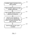
In FIG. 3 that is a flow chart illustrating a illustrating according to a third preferred embodiment of the present invention, the method for fabricating an LCD begins at step 301.
At step 301, the MAV organic monomers 2 are coated on the glass substrate 1.
At step 302, the MAV organic monomers 2 are patterned through a photomask 3.
At step 303, the MAV organic monomers 2 which are not patterned on the glass substrate 1 are filtered.
At step 304, the glass substrate 1 is cleaned for removing the non-patterned MVA organic monomers 2 remaining in the glass substrate 1.
At step 305, the MAV organic monomers 2 which have been patterned are cured.
After the MAV organic monomers 2 which are not patterned on the glass substrate 1 are filtered completely in the method for fabricating an LCD of the present invention, The glass substrate 1 is cleaned by using organic solvents for removing the non-patterned MVA organic monomers 2 remaining in the glass substrate 1. Thus, the effect of the MAV layer for the liquid-crystal molecules can be assured, and the vertical alignment of the liquid-crystal molecules does not be affected by the remaining MVA organic monomers 2.
In the method for fabricating an LCD according to the preferred embodiment of the present invention, the MAV organic monomers 2 are non-solvent type photocurable organic monomers. Because the MAV organic monomers 2 are non-solvent type photocurable organic monomers, it can be utilized without dissolving in a solvent, whereby there is no by-product of macromolecules formed during the photo-curing process. Therefore, the curing process is more complete, safe and easier in the curing operation without regarding to the treatment of the by-products.
In comparison with the conventional processes, the method for fabricating an LCD of the present invention has the advantages of simple processes, environmental protection, low technical difficulty, and so on, and the manufacturing cost of the LCD can be effectively reduced.
While the preferred embodiments of the present invention have been illustrated and described in detail, various modifications and alterations can be made by persons skilled in this art. The embodiment of the present invention is therefore described in an illustrative but not restrictive sense. It is intended that the present invention should not be limited to the particular forms as illustrated, and that all modifications and alterations which maintain the spirit and realm of the present invention are within the scope as defined in the appended claims.

Claims (13)

What is claimed is:
1. A method for fabricating an LCD, comprising fabricating a multi-domain vertical alignment (MAV) layer on a glass substrate, characterized in that, the step of fabricating the MAV layer on the glass substrate comprises the steps of:
(A) coating MAV organic monomers on the glass substrate;
(B) patterning the MAV organic monomers through a photomask for forming a trapezoid region on the glass substrate;
(C) curing the trapezoid region of the patterned MAV organic monomers;
the MAV organic monomers having a viscosity of 5 to 500 mPa·s and a coating thickness of 800 to 1800 nanometers at the step (A);
a distance between the photomask and a surface of the MAV organic monomers being 0.3-50 micrometers at the step (B);
a light for performing the patterning at the step (B) having a wavelength between 100 to 780 nanometers with an exposure time between 30 to 540 seconds;
after the step (B) and before the step (C), the method further comprising the steps of:
(B1) filtering the MAV organic monomers which are not patterned on the glass substrate; and
(B2) cleaning the glass substrate for removing the non-patterned MAV organic monomers remaining on the glass substrate;
the step (C) specifically comprising photo-curing and/or heat treating the patterned MAV organic monomers;
a wavelength of a light of the photo-curing being between 100 to 780 nanometers with an exposure duration between 30 to 540 seconds;
a temperature of the heat treatment being between 50 to 250 degrees with a treatment duration between 30 to 540 seconds;
the MAV organic monomers being non-solvent type photocurable organic monomers.
2. A method for fabricating an LCD, comprising fabricating a multi-domain vertical alignment (MAV) layer on a glass substrate, characterized in that, the step of fabricating the MAV layer on the glass substrate comprises the steps of:
(A) coating MAV organic monomers on the glass substrate, wherein the MAV organic monomers are non-solvent type photocurable organic monomers;
(B) patterning the MAV organic monomers through a photomask for forming a trapezoid region on the glass substrate; and
(B1) filtering the MAV organic monomers which are not patterned on the glass substrate; and
(C) curing the trapezoid region of the patterned MAV organic monomers.
3. The method for fabricating an LCD according to claim 2, characterized in that the MAV organic monomers have a viscosity of 5 to 500 mPa·s and a coating thickness of 800 to 1800 nanometers at the step (A).
4. The method for fabricating an LCD according to claim 2, characterized in that a distance between the photomask and a surface of the MAV organic monomers are 0.3-50 micrometers at the step (B).
5. The method for fabricating an LCD according to claim 2, characterized in that a light for performing the patterning at the step (B) has a wavelength between 100 to 780 nanometers with an exposure time between 30 to 540 seconds.
6. The method for fabricating an LCD according to claim 2, characterized in that after the step (B1) and before the step (C), the method further comprises the step of:
(B2) cleaning the glass substrate for removing the non-patterned MAV organic monomers remaining on the glass substrate.
7. The method for fabricating an LCD according to claim 3, characterized in that after the step (B) and before the step (C), the method further comprises the steps of:
(B1) filtering the MAV organic monomers which are not patterned on the glass substrate; and
(B2) cleaning the glass substrate for removing the non-patterned MAV organic monomers remaining on the glass substrate.
8. The method for fabricating an LCD according to claim 4, characterized in that after the step (B) and before the step (C), the method further comprises the steps of:
(B1) filtering the MAV organic monomers which are not patterned on the glass substrate; and
(B2) cleaning the glass substrate for removing the non-patterned MAV organic monomers remaining on the glass substrate.
9. The method for fabricating an LCD according to claim 5, characterized in that after the step (B) and before the step (C), the method further comprises the steps of:
(B1) filtering the MAV organic monomers which are not patterned on the glass substrate; and
(B2) cleaning the glass substrate for removing the non-patterned MAV organic monomers remaining in the glass substrate.
10. The method for fabricating an LCD according to claim 2, characterized in that the step (C) specifically comprises photo-curing and/or heat treating the patterned MAV organic monomers.
11. The method for fabricating an LCD according to claim 10, characterized in that a wavelength of a light of the photo-curing is between 100 to 780 nanometers with an exposure duration between 30 to 540 seconds.
12. The method for fabricating an LCD according to claim 10, characterized in that a temperature of the heat treatment is between 50 to 250 degrees with a treatment duration between 30 to 540 seconds.
13. The method for fabricating an LCD according to claim 11, characterized in that a temperature of the heat treatment is between 50 to 250 degrees with a treatment duration between 30 to 540 seconds.
US13/375,227 2011-10-14 2011-10-26 Method for fabricating LCD Active 2032-03-30 US8753799B2 (en)

Applications Claiming Priority (4)

Application Number Priority Date Filing Date Title
CN2011103127509A CN102368129B (en) 2011-10-14 2011-10-14 Manufacturing method of liquid crystal display
CN201110312750 2011-10-14
CN201110312750.9 2011-10-14
PCT/CN2011/080842 WO2013053136A1 (en) 2011-10-14 2011-10-26 Method for fabricating liquid crystal display

Publications (2)

Publication Number Publication Date
US20130095430A1 US20130095430A1 (en) 2013-04-18
US8753799B2 true US8753799B2 (en) 2014-06-17

Family

ID=45760699

Family Applications (1)

Application Number Title Priority Date Filing Date
US13/375,227 Active 2032-03-30 US8753799B2 (en) 2011-10-14 2011-10-26 Method for fabricating LCD

Country Status (3)

Country Link
US (1) US8753799B2 (en)
CN (1) CN102368129B (en)
WO (1) WO2013053136A1 (en)

Families Citing this family (2)

* Cited by examiner, † Cited by third party
Publication number Priority date Publication date Assignee Title
CN106353925A (en) * 2016-11-01 2017-01-25 深圳市瑞福达液晶显示技术股份有限公司 Method for manufacturing high-duty cycle vertical orientation liquid crystal display device
CN110187564A (en) * 2019-05-21 2019-08-30 深圳市华星光电技术有限公司 A kind of display panel and preparation method thereof

Citations (3)

* Cited by examiner, † Cited by third party
Publication number Priority date Publication date Assignee Title
US20090316096A1 (en) * 2000-06-20 2009-12-24 Alessandro Cesare Callegari Multi-domain and ips liquid-crystal display using dry alignment
US20100059709A1 (en) * 2006-12-22 2010-03-11 Rolic Ag Patternable liquid crystal polymer comprising thio-ether units
US20110189597A1 (en) * 2010-01-29 2011-08-04 Chunghwa Picture Tubes, Ltd. Method of forming exposure patterns

Family Cites Families (12)

* Cited by examiner, † Cited by third party
Publication number Priority date Publication date Assignee Title
TW515926B (en) * 1996-07-10 2003-01-01 Matsushita Electric Ind Co Ltd Liquid crystal alignment film and method for producing the same, and liquid crystal display apparatus using the same and method for producing the same
US5739883A (en) * 1996-08-30 1998-04-14 Nan Ya Technology Corporation Manufacturing method and structure for aligner of liquid crystal display
KR20010024339A (en) * 1997-10-01 2001-03-26 모리시타 요이찌 Liquid crystal alignment film and method of producing the same, and liquid crystal display using the same and method of producing the same
JPH11218763A (en) * 1998-02-03 1999-08-10 Hitachi Ltd Production of liquid crystal display element
JP2001290154A (en) * 2000-04-06 2001-10-19 Jsr Corp Resin film and liquid crystal alignment treatment method
KR100804849B1 (en) * 2001-10-16 2008-02-20 다이니폰 인사츠 가부시키가이샤 Method of producing optical element by patterning of liquid crystal films
CN100476548C (en) * 2004-01-10 2009-04-08 中国科学院长春光学精密机械与物理研究所 Method for preparing liquid crystal vertical oriented membrane
KR101017157B1 (en) * 2004-06-30 2011-02-25 엘지디스플레이 주식회사 Liquid Crystal Display device and the fabrication method
TWI395993B (en) * 2008-06-30 2013-05-11 Au Optronics Corp Liquid crystal display panel and composition of liquid crystal layer thereof
TWI372294B (en) * 2008-07-21 2012-09-11 Au Optronics Corp Liquid crystal display panel and fabricating method thereof
WO2010137386A1 (en) * 2009-05-27 2010-12-02 シャープ株式会社 Liquid crystal display device
CN101957521B (en) * 2010-08-12 2013-11-20 大连东方科脉电子有限公司 High-contrast liquid crystal electronic paper displayer and manufacturing method thereof

Patent Citations (3)

* Cited by examiner, † Cited by third party
Publication number Priority date Publication date Assignee Title
US20090316096A1 (en) * 2000-06-20 2009-12-24 Alessandro Cesare Callegari Multi-domain and ips liquid-crystal display using dry alignment
US20100059709A1 (en) * 2006-12-22 2010-03-11 Rolic Ag Patternable liquid crystal polymer comprising thio-ether units
US20110189597A1 (en) * 2010-01-29 2011-08-04 Chunghwa Picture Tubes, Ltd. Method of forming exposure patterns

Also Published As

Publication number Publication date
CN102368129A (en) 2012-03-07
US20130095430A1 (en) 2013-04-18
CN102368129B (en) 2013-06-26
WO2013053136A1 (en) 2013-04-18

Similar Documents

Publication Publication Date Title
TWI429996B (en) Apparatus and method of fabricating alignment layer for liquid crystal display, and the crystal display using the same
CN102981314B (en) The preparation method of alignment film
US20180157126A1 (en) Alignment method suitable for psva liquid crystal display panel
WO2016176930A1 (en) Color filter, manufacturing method therefor, and liquid crystal display device
US8810898B2 (en) Micro-cup substrate preparation method and display device thereof
US8753799B2 (en) Method for fabricating LCD
WO2016029516A1 (en) Method for manufacturing pairing marks of cf substrate
CN104932148B (en) Composite substrate, liquid crystal display screen and manufacturing method
WO2015070609A1 (en) Method for manufacturing color film substrate, color film substrate, and display apparatus
US20150079279A1 (en) Method for manufacturing color filter
CN106773334B (en) Method for preparing display panel and prepared display panel
KR20180059530A (en) Method of manufacturing display panel and liquid crystal display
CN110456555B (en) Color filter and preparation method thereof
CN102636912B (en) Liquid crystal indicator and preparation method thereof
CN101840111A (en) Manufacturing method of oriented film and LCD panel
CN109343259B (en) Liquid crystal lens and preparation method thereof
US10564451B2 (en) Panel and method for manufacturing the same
KR102200338B1 (en) Method for forimg polyimide layer and method for fabricating liquid crystal display device using the same
KR100506072B1 (en) Fabrication method of Liquid Crystal Display
US20170285412A1 (en) Method for manufacturing liquid crystal display panel
JP5831328B2 (en) Color filter for liquid crystal display
KR100697389B1 (en) Method for fabricating polymer dispersed liquid crystal display device
TWI432798B (en) Color filter and method for manufacturing the same
US9740051B2 (en) Display substrate and manufacturing method thereof, liquid crystal cell as well as display
CN111781775A (en) Preparation method of liquid crystal micro-lens array based on thickness gradient distribution orientation film

Legal Events

Date Code Title Description
AS Assignment

Owner name: SHENZHEN CHINA STAR OPTOELECTRONICS TECHNOLOGY CO.

Free format text: ASSIGNMENT OF ASSIGNORS INTEREST;ASSIGNOR:WANG, JUN;REEL/FRAME:027306/0442

Effective date: 20111028

STCF Information on status: patent grant

Free format text: PATENTED CASE

FEPP Fee payment procedure

Free format text: PAYOR NUMBER ASSIGNED (ORIGINAL EVENT CODE: ASPN); ENTITY STATUS OF PATENT OWNER: LARGE ENTITY

MAFP Maintenance fee payment

Free format text: PAYMENT OF MAINTENANCE FEE, 4TH YEAR, LARGE ENTITY (ORIGINAL EVENT CODE: M1551)

Year of fee payment: 4

MAFP Maintenance fee payment

Free format text: PAYMENT OF MAINTENANCE FEE, 8TH YEAR, LARGE ENTITY (ORIGINAL EVENT CODE: M1552); ENTITY STATUS OF PATENT OWNER: LARGE ENTITY

Year of fee payment: 8