US8748950B2 - On-demand nanoelectronics platform - Google Patents
On-demand nanoelectronics platform Download PDFInfo
- Publication number
- US8748950B2 US8748950B2 US13/509,538 US201013509538A US8748950B2 US 8748950 B2 US8748950 B2 US 8748950B2 US 201013509538 A US201013509538 A US 201013509538A US 8748950 B2 US8748950 B2 US 8748950B2
- Authority
- US
- United States
- Prior art keywords
- electron gas
- nanoscale
- reconfigurable
- tip
- insulating layer
- Prior art date
- Legal status (The legal status is an assumption and is not a legal conclusion. Google has not performed a legal analysis and makes no representation as to the accuracy of the status listed.)
- Active, expires
Links
Images


Classifications
-
- H—ELECTRICITY
- H10—SEMICONDUCTOR DEVICES; ELECTRIC SOLID-STATE DEVICES NOT OTHERWISE PROVIDED FOR
- H10D—INORGANIC ELECTRIC SEMICONDUCTOR DEVICES
- H10D62/00—Semiconductor bodies, or regions thereof, of devices having potential barriers
- H10D62/10—Shapes, relative sizes or dispositions of the regions of the semiconductor bodies; Shapes of the semiconductor bodies
- H10D62/117—Shapes of semiconductor bodies
- H10D62/118—Nanostructure semiconductor bodies
-
- B—PERFORMING OPERATIONS; TRANSPORTING
- B82—NANOTECHNOLOGY
- B82Y—SPECIFIC USES OR APPLICATIONS OF NANOSTRUCTURES; MEASUREMENT OR ANALYSIS OF NANOSTRUCTURES; MANUFACTURE OR TREATMENT OF NANOSTRUCTURES
- B82Y10/00—Nanotechnology for information processing, storage or transmission, e.g. quantum computing or single electron logic
-
- H—ELECTRICITY
- H10—SEMICONDUCTOR DEVICES; ELECTRIC SOLID-STATE DEVICES NOT OTHERWISE PROVIDED FOR
- H10D—INORGANIC ELECTRIC SEMICONDUCTOR DEVICES
- H10D30/00—Field-effect transistors [FET]
- H10D30/60—Insulated-gate field-effect transistors [IGFET]
-
- H—ELECTRICITY
- H10—SEMICONDUCTOR DEVICES; ELECTRIC SOLID-STATE DEVICES NOT OTHERWISE PROVIDED FOR
- H10F—INORGANIC SEMICONDUCTOR DEVICES SENSITIVE TO INFRARED RADIATION, LIGHT, ELECTROMAGNETIC RADIATION OF SHORTER WAVELENGTH OR CORPUSCULAR RADIATION
- H10F30/00—Individual radiation-sensitive semiconductor devices in which radiation controls the flow of current through the devices, e.g. photodetectors
- H10F30/20—Individual radiation-sensitive semiconductor devices in which radiation controls the flow of current through the devices, e.g. photodetectors the devices having potential barriers, e.g. phototransistors
- H10F30/21—Individual radiation-sensitive semiconductor devices in which radiation controls the flow of current through the devices, e.g. photodetectors the devices having potential barriers, e.g. phototransistors the devices being sensitive to infrared, visible or ultraviolet radiation
- H10F30/28—Individual radiation-sensitive semiconductor devices in which radiation controls the flow of current through the devices, e.g. photodetectors the devices having potential barriers, e.g. phototransistors the devices being sensitive to infrared, visible or ultraviolet radiation the devices being characterised by field-effect operation, e.g. junction field-effect phototransistors
- H10F30/282—Insulated-gate field-effect transistors [IGFET], e.g. MISFET [metal-insulator-semiconductor field-effect transistor] phototransistors
-
- H—ELECTRICITY
- H10—SEMICONDUCTOR DEVICES; ELECTRIC SOLID-STATE DEVICES NOT OTHERWISE PROVIDED FOR
- H10F—INORGANIC SEMICONDUCTOR DEVICES SENSITIVE TO INFRARED RADIATION, LIGHT, ELECTROMAGNETIC RADIATION OF SHORTER WAVELENGTH OR CORPUSCULAR RADIATION
- H10F77/00—Constructional details of devices covered by this subclass
- H10F77/10—Semiconductor bodies
- H10F77/14—Shape of semiconductor bodies; Shapes, relative sizes or dispositions of semiconductor regions within semiconductor bodies
- H10F77/143—Shape of semiconductor bodies; Shapes, relative sizes or dispositions of semiconductor regions within semiconductor bodies comprising quantum structures
- H10F77/1437—Quantum wires or nanorods
Definitions
- semiconductors as technologically useful materials is based on features such as: the electrical conductivity of the semiconductor, especially the ability to readily tune the conductivity of the semiconductor materials; the ability to readily create insulating layers that would enable the fabrication of field-effect devices; and the ability to reproducibly create various field-effect devices having nanoscale dimensions.
- Oxide materials have been identified that combine many of the important electronic properties of semiconductors, such as interfacial superconductivity, strain-driven ferroelectricity, interfacial ferromagnetism, and colossal magnetoresistance.
- a reconfigurable device including a first insulating layer and a second insulating layer; and a nanoscale quasi one- or zero-dimensional electron gas disposed at an interface between the first and second insulating layers, wherein the device is reconfigurable by applying an external electrical field to the electron gas to change the conductivity of the electron gas.
- the reconfigurable device further comprises at least one other nanoscale quasi one- or zero-dimensional electron gas region, wherein said at least two electron gas regions are configured in a substantially cross shape, and wherein the reconfigurable device is configured as a magnetic field sensor.
- said first and second insulating layers include a polar insulating layer and a non-polar insulating layer, wherein the nanoscale quasi one- or zero-dimensional electron gas has a gap formed therein, and wherein the reconfigurable device is configured as a reconfigurable photodetector.
- the photodetector can further comprise a gate electrode disposed adjacent the gap.
- the photodetector further comprises a plurality of quasi one-dimensional electron gas regions forming a plurality of nanowires each having a gap thereon, wherein the reconfigurable device is configured as a photodetector array.
- said interface extends a few unit cells into one of the first or second insulating layers. For example, said interface extends about 3 unit cells into one of the first or second insulating layers.
- the electron gas region comprises at least one memory cell, and wherein the reconfigurable device is configured as a memory device.
- the reconfigurable device further comprises a plurality of nanoscale wires formed with electron gas regions, and wherein the reconfigurable device is configured as a reconfigurable transistor.
- a reconfigurable transistor comprises a first nanoscale wire; a second nanoscale wire disposed substantially along the direction of the first nanoscale wire, wherein a gap between the first and second nanowares have a first length; and a third nanoscale wire disposed along a direction substantially different from the direction of the first or second nanaoscale wire, wherein an end of the third nanoscale wire has a second distance to the gap larger than the first distance.
- the first, second, and third nanoscale wire comprise quasi-one dimensional or two dimensional electron gas disposed at an interface between a polar material and a non-polar material.
- the polar insulating layer comprises LaAlO 3
- the non-polar insulating layer comprises SrTiO 3 .
- the first nanoscale wire is coupled to a source electrode
- the second nanoscale wire is coupled to a drain electrode
- the third electrode is coupled to a gate electrode
- the direction of the third nanoscale wire is substantially orthogonal to the direction of the first or second nanoscale wire.
- each of the first, second, and third nanoscale wire is removable or reconfigurable in its respective length, width, and position by an external electric field applied to the reconfigurable transistor.
- a magnetic field sensor including at least two nanoscale quasi one- or zero-dimensional electron gas regions disposed at interfaces between insulating layers, wherein the at least two electron gas regions are configured in a substantially cross shape.
- a photodetector including a nanoscale wire formed at an interface between SrTiO 3 and LaAlO 3 .
- a reconfigurable transistor including a first nanoscale wire, a second nanoscale wire disposed substantially along the direction of the first nanoscale wire, wherein a gap between the first and second nanowares have a first length, and a third nanoscale wire disposed along a direction substantially different from the direction of the first or second nanoscale wire, wherein an end of the third nanoscale wire has a second distance to the gap larger than the first distance.
- the first, second, and third nanoscale wire can include quasi-one dimensional or two dimensional electron gas disposed at an interface between a polar material and a non-polar material.
- the polar insulating layer can comprise LaAlO 3
- the non-polar insulating layer can comprise SrTiO 3 .
- the first nanoscale wire can be coupled to a source electrode
- the second nanoscale wire can be coupled to a drain electrode
- the third electrode can be coupled to a gate electrode.
- the direction of the third nanoscale wire is substantially orthogonal to the direction of the first or second nanoscale wire.
- Each of the first, second, and third nanoscale wires is removable or reconfigurable in its respective length, width, and position by an external electric field applied to the reconfigurable transistor.
- a method including forming a nanoscale quasi one- or zero-dimensional electron gas region disposed at an interface between a first and a second insulating layers, and applying an external electrical field to the electron gas region to change a conductivity of the electron gas region.
- the first and a second insulating layers include a polar insulating layer and a non-polar insulating layer.
- the method further includes forming a substantially T-shaped electron gas region at an interface between a polar insulating layer and a non-polar insulating layer, erasing a center portion of the T-shaped electron gas region with an external electric field thereby forming a source terminal, a drain terminal, and a gate terminal, forming a nanoscale wire between the source and drain contacts wherein the nanoscale wire is substantially narrower than the T-shaped electron gas region, and forming a gap between the source and drain terminals, thereby forming a reconfigurable transistor.
- said forming a substantially T-shaped electron gas region comprises applying an external electric field to the interface at a first voltage
- said forming a nanoscale wire comprises applying an external electric field to the interface at a second voltage
- said forming a gap comprises applying an external electric field to the interface at a second voltage, wherein the first and second voltages are positive, wherein the third voltage is negative, and wherein the second and third voltages have values substantially smaller than that of the first voltage.
- said applying an external electric field comprises applying an electric field from an atomic force microscope (AFM).
- AFM atomic force microscope
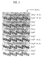
- FIG. 1 is a schematic diagram of the LaAlO 3 /SrTiO 3 heterostructure.
- the oxide heterostructure comprises alternating layers of (AlO 2 ) ⁇ ( 1 ) and (LaO) + ( 3 ), so as to form a polar insulating layer of lanthanum aluminate that is grown epitaxially onto a non-polar strontium titanate insulating layer formed of alternating SrO ( 5 ) and TiO 2 ( 7 ) layers.
- FIG. 2A is a schematic diagram for creating nanostructures, such as a wire nanostructure, using a conducting AFM probe ( 10 ).
- a voltage-biased AFM tip ( 20 ) is scanned from one electrode ( 30 ) towards a second electrode ( 40 ) in contact mode.
- the tip ( 20 ) generates an electric field that causes a metallic quasi-1DEG (q-1DEG) to form locally at the interface between the LaAlO 3 and SrTiO 3 layers.
- q-1DEG metallic quasi-1DEG
- FIG. 2B is a graph of conductance as a function of the tip ( 20 ) position while writing a conducting wire ( 50 ) with a 3V bias applied to the tip. A steep increase in conductance occurs when the tip reaches the second electrode ( 40 ).
- FIG. 2C is a schematic diagram of the experimental set up for cutting a conducting wire.
- a negatively biased AFM tip ( 20 ) moves in contact mode across the conducting wire ( 50 ).
- the tip erases the metallic q-1DEG locally when it crosses the conducting wire.
- the conductance between the two electrodes ( 30 , 40 ) is monitored as the tip scans over the wire ( 50 ).
- FIG. 2D is a graph of the conductance between the two electrodes ( 30 , 40 ) as a function of the tip ( 20 ) position across the wire ( 50 ), while cutting the wire with the tip biased at ⁇ 3V.
- a sharp drop in conductance is observed when the tip passes the wire ( 50 ).
- Inset shows the conductance measured over the entire 8 ⁇ m scan length.
- FIG. 3A is a schematic showing a linear array of conductive quantum dots ( 70 ) written with voltage pulses from the tip ( 20 ) of a conducting AFM.
- FIG. 3B is a graph of the conductance change as a function of dot spacing for an array of conductive quantum dots written using pulses of different durations and connecting the electrodes ( 30 , 40 ).
- FIG. 3C is a plot of minimum dot spacing for which the array is non-conducting d nc and the maximum dot spacing for which the array is conducting d c , presented as a function of pulse duration t pulse .
- FIG. 4A is a plot of the current-voltage characteristics of a LaAlO 3 /SrTiO 3 -based device.
- the current I n between the electrodes ( 30 , 40 ) is plotted as a function of the source-drain voltage (V sd ) for a 20 ⁇ m long q-1DEG wire with a potential barrier near the center and created with a negative gate bias V gate .
- V sd source-drain voltage
- FIG. 4B is a plot of the AFM tip current I_ versus tip voltage V tip with respect to grounded interface.
- FIGS. 5A-5E illustrate the creation of nanoscale tunnel barriers.
- FIG. 5A is a sketch illustrating how a potential barrier is created by scanning a negatively biased AFM probe. (Inset (A)) Either increasing the magnitude of negative tip bias (V tip ) or scanning across the wire for more times (N cut ) with the same tip bias will increase the height of potential barrier.
- FIG. 5B is an illustration of the structure used for a four-wire measurement.
- FIG. 5C is a sketch of a two-wire ac measurement scheme.
- the upper inset shows the conductance of the uncut wire (slope of the I-V curve) to be 6.8 ⁇ S.
- the lower inset shows the turn-on voltage of the nanowire section with a potential barrier as a function of the V tip that is used to create the barrier.
- the dashed line shows an exponentially decaying conductance G as a function of barrier height (G ⁇ exp [ ⁇ A′N cut ]), which is typical for thermal activated hopping.
- FIGS. 6A-6C illustrate the SketchFET device.
- FIG. 6A is a schematic diagram of SketchFET structure.
- FIG. 6C is a contour plot of I D (V SD ,V GD ). Contours are spaced 50 nA apart.
- FIG. 7A is a 5 mm ⁇ 5 mm optical image of LaAlO 3 /SrTiO 3 structure with nine electrode sets.
- FIG. 7B is a 50 ⁇ m ⁇ 50 ⁇ m AFM image showing ends of four Au electrodes and central writable area.
- FIG. 7C is a 1 ⁇ m ⁇ 1 ⁇ m AFM image showing ⁇ 3 ⁇ terrace structure due to the substrate miscut.
- FIG. 9A shows a perspective view of a T-Junction.
- FIG. 9C shows further currents between source and drain under various V GD and V GD .
- FIG. 10 illustrates, for the SketchFET structure, I-V characteristic between source and drain (I SD ) plotted together with I-V characteristic between gate and drain (I GD ).
- FIG. 11 illustrates I-V characteristics of a SketchFET with a larger barrier. Drain current I D is plotted as a function of source bias V SD at various gate biases V GD , showing a more pronounced field effect.
- FIG. 12A is a schematic diagram of frequency response measurement.
- FIG. 12B shows normalized frequency response of SketchFET and a commercial NPN small signal transistor (cut-off frequency is 900 MHz) with no external resistor and resistors of 500 ⁇ , 10 k ⁇ , or 1 M ⁇ connected in series with the emitter.
- FIG. 13 illustrates power gain of a SketchFET structure as a function of source bias V SD plotted for various values of the gate bias V GD .
- FIG. 14A is a perspective view of the overall geometry of the Hall cross used as a Hall sensor.
- FIG. 14B is a close-up view of the Hall sensor.
- FIG. 14C illustrate the Hall voltage measured as a function of applied magnetic field.
- FIG. 15B shows a close-up view of the Hall voltage curve illustrating sensitivity of the Hall voltage to small magnetic fields.
- FIG. 15C shows a further close-up view of the Hall voltage curve, where the slope of the curve in quantifies how rapidly the Hall voltage changes with the applied magnetic field.
- FIG. 15D shows noise in Hall signal measured away from the peak, used to calculate the signal-to-noise for this system.
- the inset shows nanowire writing at the LaAlO 3 /SrTiO 3 interface. Buried Au electrodes are directly contacted to the interface. A positive voltage applied to the conducting atomic force microscope (c-AFM) probe will locally switch the interface to a conducting state, while a negative voltage will locally restore the insulating state.
- c-AFM conducting atomic force microscope
- FIGS. 17A-17 C illustrate the operation of SketchFET at GHz frequencies.
- FIG. 17 A illustrates the electrical schematic of mixing heterodyne experiment.
- Microwaves at frequency f plus a DC bias V SD are applied to the source electrode; microwaves at frequency f+df plus a DC bias V GD are applied to the gate electrode.
- the drain current i D is measured with a lock-in amplifier at frequency df.
- FIG. 18A is an intensity plot of fitting parameters i df , as a function of V SD and V GD .
- FIG. 18B is an intensity plot of fitting parameters f T , as a function of V SD and V GD .
- FIG. 18C is an intensity plot of fitting parameters f C as a function of V SD and V GD .
- the symbols represent the bias conditions shown in FIGS. 18B and 18C and in Table 2.
- P RF 0 dBm.
- FIG. 19 is a schematic diagram illustrating the nanowriting process at the LaAlO 3 /SrTiO 3 interface.
- Au electrodes shown connected to V s and I D ) are electrically contacted to the LaAlO 3 /SrTiO 3 interface.
- the AFM tip with an applied voltage is scanned once between the two electrodes with a voltage applied V tip (x(t), y(t)). Positive voltages locally switch the interface to a conducting state, while negative voltages locally restore the insulating state.
- a conducting nanowire is being written.
- the conductance between the two electrodes is monitored by applying a small voltage bias on one of the two gold electrodes (V s ) and reading the current at the second electrode (I D ).
- FIG. 20 illustrates structure and electrical properties of non-reciprocal nanoscale devices at the LaAlO 3 /SrTiO 3 interface.
- the substantially linear curve indicates I-V curve before the first cut. Intermediate I-V curves are shown after every alternate cut. As the wire is cut, the potential barrier increases (inset), and the zero-bias conductance decreases; however, the overall I-V curve remains highly reciprocal.
- FIG. 21B are I-V plots for a nanowire subject to a sequence of cuts N cut (x) at nine locations spaced 5 nm apart along the nanowire (see Table 3).
- the substantially linear curve indicates I-V curve before the first cut.
- the asymmetry in N cut (x) results in a non-reciprocal I-V curve.
- FIG. 22 includes a diagram of a sample and a photoresponse.
- (a) A schematic illustration of how a c-AFM tip writes a nanowire at the interface between LaAlO 3 and SrTiO 3 .
- FIG. 23 shows scanning photocurrent microscopy (SPCM) images of various nanostructures written at the LaAlO 3 /SrTiO 3 interface. Images are 50 ⁇ 50 mm 2 . Dashed lines indicate boundaries of areas where electrical contact is made to the LaAlO 3 /SrTiO 3 interface; solid lines indicate the locations of nanowires.
- SPCM image of area before any nanostructures are written.
- SPCM image for a nanowire junction written close to a pair of electrodes.
- FIG. 24 illustrates a three-terminal, nanoscale, locally gateable photodetector.
- V SD and V GD respectively
- Simultaneously acquired reflectivity image Dashed lines show outlines of electrodes. Solid lines represent nanostructures written with a c-AFM. Both the nanowire widths and gap separations are exaggerated for clarity. Scan size is 50 ⁇ 50 mm 2 .
- FIG. 26 shows spectral sensitivity and intensity dependence from visible to near-infrared wavelengths.
- Responsivity of the photodetector from 532 nm to 1,340 nm. Symbols are derived from Gaussian fits of SPCM images; lines are guides to the eye.
- Photocurrent versus optical intensity for different laser wavelengths Lines are power-law fits. The inset shows the power-law exponent m as a function of wavelength. Error bars represent one standard deviation from the best fit value.
- the embodiments described here relate to devices characterized by having nanoscale dimensions and to methodology for their creation.
- some embodiments relate to nanoscale devices comprising quasi one- or zero-dimensional electron gas at the interface between insulating oxide layers.
- electron gas refers to small isolated “puddles” of conducting electrons (see, e.g., Finkelstein, et al., Science, 2000, 289, 90), which form locally at the interface between the insulating oxide layers, pursuant to the embodiments disclosed herein, upon the application of an external electric field by means of an atomic force microscope.
- the phrase “local field” refers to an electric field that is applied to a specific nanoscale portion or region of the oxide heterostructure having one dimension smaller than 1000 nm.
- the electric field is applied to a region that is less than 100 nm wide, and preferably a region in the range from about 1 nm to about 20 nm wide.
- local metallic region refers to an electrically conductive region that has a nanoscale dimension, such as a width of 1000 nm or less.
- oxide heterostructure refers to a material system that comprises a polar insulating layer (e.g., LaAlO 3 ), grown epitaxially on to a non-polar insulating layer (e.g., SrTiO 3 ).
- the polar insulating layer has a thickness that allows metal-insulator transition to occur in the presence of an external electric field.
- the thickness of the polar LaAlO 3 layer is preferably three unit cells.
- nanoscale electrode refers to electrodes within a nanoscale portion or region of the oxide heterostructure, wherein the electrodes themselves have nanoscale dimensions.
- interconnect refers to a nanowire made using a conducting atomic force microscope to electrically connect two electronic or solid state devices, such as two transistors through an insulating layer.
- conductive region of passive device refers to a nanowire which is an electrode of a capacitor, is the conductive portion of a resistor, or winds around a magnetic region in an inductor.
- perovskite structure refers to a structure comprising the general formula ABX 3 .
- Compounds having a perovskite structure comprise 12-coordinated A 2+ atoms on the corner of a cube, octahedral X ⁇ anion in the center of the face edges, and a tetrahedral B 4+ ions in the middle of the cube.
- a perovskite structure can also be tetragonal, orthorhombic, or rhombohedral, depending on temperature.
- a material system that allows electric field-induced, metal-insulator quantum phase transitions often comprises a polar oxide layer, e.g., LaAlO 3 , LaTiO 3 , LaVO 3 or KTaO 3 , overlaying a non-polar oxide layer, such as SrTiO 3 .
- the metal-insulator transition in such a material system is due to the formation of a conductive electron gas at the interface between the insulating layers.
- the embodiments described below relate to technologically useful nanoscale devices, and to methods for forming and removing (erasing) nanoscale-conducting structures, using tools that create local electric fields.
- the tools can include, for example, a tip of a conducting atomic force microscope (AFM).
- AFM conducting atomic force microscope
- the methods allow both isolated and continuous conducting features to be formed with length in a range well below 5 nm.
- An isolated conducting feature is a conductive quantum dot as shown in FIG. 3A .
- a continuous conducting feature is exemplified by a nanowire connecting the electrodes as shown in FIG. 2A .
- a material system comprises growing a polar insulating layer of LaAlO 3 onto a TiO 2 -terminated insulating SrTiO 3 layer.
- the thickness of the LaAlO 3 layer is configured such that it allows metal-insulator transitions upon the application of an external electric field.
- the thickness is three unit cells. Samples of the oxide heterostructure prepared as described below were used for the metal-insulator transition studies. It should be noted that the thickness of the polar layer is selected such that it also allows eliminating conduction due to polar discontinuity.
- an AFM tip is used to contact the top LaAlO 3 surface.
- the AFM tip is biased at a voltage V tip with respect to the interface, and results in producing an interfacial metallic (V tip >0) or insulating (V tip ⁇ 0) state directly below the area of contact.
- FIG. 1 shows a schematic view of the LaAlO 3 /SrTiO 3 oxide heterostructure. As seen in FIG.
- the heterostructure comprises alternate layers of (AlO2) ⁇ ( 1 ) and (LaO) + ( 3 ), so as to form a polar lanthanum aluminate layer that is grown epitaxially onto a non-polar strontium titanate insulating layer formed of SrO ( 5 ) and TiO 2 ( 7 ) layers.
- FIG. 2A shows a schematic of the experimental set-up for writing a conducting wire ( 50 ) according to one embodiment.
- the material system comprises an oxide heterostructure having a set of electrodes that are placed in contact with the interface, and separated from each other by a finite distance.
- a voltage-biased tip ( 20 ) of an AFM is then scanned from one electrode ( 30 ) towards the second electrode ( 40 ) in contact mode.
- the electric field generated by the tip causes a metallic quasi-1 or 0-dimensional electron gas (q-1DEG or q-0DEG) to form locally at the interface ( 100 ) between the LaAlO 3 and SrTiO 3 layers.
- the AFM tip was biased at a voltage of 3V, and a lock-in amplifier was used to measure the conductance between the two electrodes. As shown in FIG. 2B , the measured conductance changes as a function of the tip position. Moving the AFM tip in contact mode towards the second electrode results in a steep increase in measured conductance with a maximum conductance occurring when the AFM tip reaches the second electrode.
- a method is also provided for creating and erasing nanowires and quantum dots using a conducting AFM tip ( 20 ) to create localized electrically conductive regions at the interface of the insulating layers.
- the nanowires can have a width less than 20 nm, more preferably a width in the range of about 3.3 nm to about 10 nm and even more preferably a width less than 6 nm, 5 nm, and 4 nm. In one embodiment, the nanowire has a width of about 2.1 nm.
- the quasi-one-dimensional electrically conductive region has a length in the range of about 100 nm to about 100 ⁇ m, more preferably a length in the range of about 100 nm to at least about 10 ⁇ m, and even more preferably a length less than 700 nm, 600 nm, 500 nm, 400 nm, 300 nm, and 200 nm.
- the nanowire has a length of at least about 100 nm.
- Conductive quantum dots can be formed with a diameter or width less than about 20 nm.
- the conductive quantum dots Preferably have a width or diameter in the range from about 1 nm to about 10 nm.
- the conductive region formed at the interface of the insulating layers can retain its conductivity for a sufficiently long time interval after the withdrawal of the first external local electric field to provide useful function.
- Conductivity can be retained, for example, for at least about 12 h and more preferably from at least about 12 h to at least about 24 h. In some embodiments the conductive region retains its conductivity for a time interval greater than 24 h.
- the nanowires or quantum dots are buried at the interface of the two insulating materials.
- the nanowire or quantum dot is formed from the so-called one- or zero-dimensionally confined electron gas at the interface, it is possible that a physical arrangement or rearrangement of atoms at the interface may also contribute to or form the nanowire or quantum dot.
- a method for measuring the transverse dimension of a conducting nanowire is also provided.
- V tip ⁇ 3 V
- the measured conductance decreases abruptly as seen from the graph in FIG. 2D .
- the diameter of the nanowire can be determined from the plot of the deconvolved differential profile (dG/dx)* ⁇ 1 as a function of tip position.
- SETs single-electron transistors
- SET's require ultra-small capacitance quantum dots, namely, dots smaller than 10 nm to operate at room temperature. Quantum dots having these dimensions are already within the reach using the method embodiments.
- the embodiments provide a method of creating nanoscale devices that permit high density data storage. For example, nanowires with a width in the range from about 3.3 nm to about 10 nm can be formed.
- an array of “dots” was created by pulsing the oxide heterostructure using the tip of a conducting AFM. This allowed small isolated “puddles” of conducting electrons that form locally at the interface between the two insulating layers. The resultant array of q-0DEG quantum dots was visualized using Kelvin probe microscopy for analyzing the spatial resolution of the array of dots.
- a linear array of “quantum dots” ( 70 ) is written as shown in FIG. 3A .
- Dots were created by applying voltage pulses V tip (t) having an amplitude V pulse and pulse duration t pulse to the tip ( 20 ) of the AFM while keeping the tip position fixed.
- the size of the dots created depends on the amplitude as well as the duration of the applied pulse. In one exemplary embodiment, V pulse was fixed at 10 V while the duration of the pulse was varied to change the size of the dots.
- To determine the effective dot size a linear array of dots at various separation distances “d” between two adjacent dots was created. The two ends of the linear array are then contacted to two conducting electrodes and the conductance between the two electrodes is monitored using a lock-in amplifier.
- the dots do not overlap and no increase in conductance is observed. However, once the spacing between dots becomes equal to or less than the dot diameter, the linear array will form a conducting wire, and an abrupt increase in conductance between the two electrodes ( ⁇ G) is observed.
- FIG. 3B graphically depicts the resultant change in conductance as a function of separation distance “d” between dots for different durations of the pulse, (t pulse ) applied with the tip of the AFM.
- t pulse the pulse applied with the tip of the AFM.
- a sharp metal-insulator transition is observed as the dot spacing is reduced.
- the metal-insulator transition occurs at a relatively larger separation distance “d,” while for the arrays created with pulses of shorter duration, the metal-insulator transition occurs at a smaller separation distance “d” between dots.
- pulses of a short duration result in smaller dots which would allow a higher density of the conducting quantum dots to be created in a given area. This would translate to media (chips) capable of ultra high density data storage.
- FIG. 3C depicts plots of the smallest non-conducting spacing ( d nc ) and the largest conducting spacing d c between dots as a function of t pulse .
- the critical spacing for conduction “d c ” scales linearly with pulse duration until pulse durations of less than a millisecond are used (t pulse ⁇ 1 ms). Below this threshold for pulse duration, the critical spacing between dots in a linear array levels off at a distance d c ⁇ 1 nm.
- a spacing between quantum dots of 7 to 15 nm corresponds to data storage capacity of >3 Tb/in 2 . Since the embodiments provide dot spacing of less than 2 nm, an improvement over the magnetic storage materials currently used in hard disk drives is provided. In some embodiments, the method allows creating small size structures (e.g., nanowires and conductive quantum dots). Thus, one might call the embodiment a “nanoelectronic sketchpad” or “quantum etch-a-sketch.”
- the width of the conducting wire can depend on the voltage of the AFM's tip (V tip ). Increasing V tip from 3 V to 10 V can increase the width of the conducting wire by three orders of magnitude. Test measurements have shown that the conductive wires created using an AFM tip remain stable over a 24 h time interval after the removal of the external electric field. Thus, it is possible to create nanoscale conducting structures in devices at room temperature using the method disclosed herein.
- a “non-volatile” field-effect transistors can be provided.
- the oxide heterostructure can be contacted with a set of electrodes at the interface of the two insulating layers. One electrode serves as the source while the second electrode functions as the drain of the FET.
- a conducting wire is written between the two electrodes and is in contact with the electrode at its opposite ends.
- the conducting tip of an AFM is then used to perturb the conductance through the application of an external electric field. In this case, the tip of the AFM acts as the “gate” of the FET.
- FIG. 4A shows the current-voltage (I-V) characteristics of a q-1DEG wire that is being perturbed by the AFM probe at varying voltages.
- Each curve in FIG. 4A represents a different applied voltage (V gate ) for the AFM probe.
- V gate the in-plane current I ll is measured (using a picoammeter referenced to virtual ground) as a function of the source-drain voltage (V sd ) applied to one of the electrodes.
- the conductance of the nano wire is unaffected.
- the methods disclosed herein allow creating exceptionally small sized electrically conductive regions in a reproducible manner using the tip of a conducting AFM as a source for applying the external electric field.
- This permits creating exceptionally small-sized, q-1 or 0-dimensional electron gas regions with high spatial resolution.
- the nanowire can be formed above, below, or on the sides of a transistor channel region, and separated from the conducting channel by a layer of insulating material, such as the perovskite insulating layer on which the nanowires are formed.
- the gate nanowire can be connected to a voltage or current source, such as a conductive pad connected to a voltage or current source or to a gate driver circuit.
- the channel may comprise a semiconductor region in a semiconductor layer that is located adjacent to the nanowire.
- the channel can be another q-1DEG nanowire located adjacent to the “gate” nanowire.
- the “channel” nanowire can be connected to the source and drain electrodes, which may comprise other conductive pads connected to a voltage or current source or to a bit line driver circuit.
- material systems wherein the LaAlO 3 /SrTiO 3 oxide heterostructure is grown on silicon, and a nanowire is used as a gate to form very high mobility devices in silicon-on insulator or strained silicon-on insulator platforms.
- the embodiments also provide various uses for the LaAlO 3 /SrTiO 3 material systems for technological applications in, for example, the use of devices in silicon-on insulator, strained silicon-on insulator or germanium-on insulator platforms as ultra-high density non-volatile data storage devices, as single electron transistors, or the use of the devices for a variety of quantum computing applications.
- the oxide heterostructure can be made by growing a LaAlO 3 layer on a TiO 2 terminated insulating SrTiO 3 substrate at 770° C. in an oxygen atmosphere at a pressure of 6 ⁇ 10 ⁇ 5 mbar using pulsed laser deposition. The samples are then cooled to 600° C. in the presence of oxygen at a pressure of 400 mbar for 1 h to give the material system comprising an oxide heterostructure.
- the thickness of the LaAlO 3 layer was varied based on the requirements for the measurements to be performed.
- the conductance of the 3 uc LaAlO 3 /SrTiO 3 sample is highly sensitive to light above the bandgap of SrTiO 3 ( ⁇ 3.2 eV).
- the 3 uc LaAlO 3 /SrTiO 3 sample exhibits a persistent photoconductivity that decays over ⁇ 12-24 hours after being stored in a dark environment.
- the 4 uc sample showed a similar photosensitivity, but the 2 uc and 0 uc samples did not exhibit photosensitivity.
- the 0 uc, 2 uc, and 3 uc samples exhibited very small background conductance of several nS, while the 4 uc sample showed a much larger background conductance ( ⁇ 1200 nS).
- Nanoscale lateral confinement of a quasi-two-dimensional electron gas at the LaAlO 3 /SrTiO 3 interface is provided. Such confinement of quasi-two-dimensional electron gas can be used to create a variety of electronic devices. Field-effect transistors can be formed with characteristic dimensions of about two nanometers. The devices can be modified or “erased” without the need for complex lithographic procedures. The on-demand nanoelectronics fabrication platform disclosed herein has the potential for widespread technological application.
- Bottom-up approaches to nanoelectronics utilize self-assembly and templated synthesis, e.g., junctions between self-assembled molecule layers metallic and semiconducting quantum dots, carbon nanotubes, nanowires, and nanocrystals.
- Top-down approaches retain the lithographic design motif used extensively at micron and sub-micron scales and make use of tools such as electron-beam lithography, atomic-force microscopy (AFM), nanoimprint lithography, dip-pen nanolithography, and scanning tunneling microscopy.
- AFM atomic-force microscopy
- the interface between polar and non-polar semiconducting oxides displays remarkable properties reminiscent of modulation-doped semiconductors.
- the thickness of the polar insulator e.g., LaAlO 3
- the potential difference across LaAlO 3 will generate a “polarization catastrophe,” due to the polarization discontinuity at the interface, and induce the formation of a quasi-two-dimensional electron gas (q-2DEG) at the interface joining the two insulators.
- q-2DEG quasi-two-dimensional electron gas
- the q-2DEG is confined largely within the first few unit cells of SrTiO 3 , with very little penetration into the LaAlO 3 layer.
- Electric fields have been used to control the metal-insulator transition at room temperature and the superconductor-insulator transition at cryogenic temperatures. Further in-plane confinement of the q-2DEG has been achieved by lithographically modulating the thickness of the crystalline LaAlO 3 layer. Control over the metal-insulator transition at ⁇ 4 nm scales was demonstrated using a conducting AFM probe.
- a device comprising nominally 3.3 unit cells (uc) of LaAlO 3 .
- a conducting AFM tip is scanned along a programmed trajectory (x(t), y(t)) with a voltage V tip (t) applied to the tip.
- V tip positive tip voltages above a threshold V tip >V t ⁇ 2-3 V produce conducting regions at the LaAlO 3 /SrTiO 3 interface below the tip of the AFM.
- the lateral size ⁇ x of this conducting nanoregion increases monotonically with tip bias.
- Subsequent erasure of the structures can be induced by scanning with a negative voltage or by illuminating with light of photon energy E>E g .
- Structures can be “written” and “erased” hundreds of times without observable degradation ( FIG. 8C ).
- the structures shown here are “written” within the same working area; similar structures have been created and measured for other electrode sets, with consistent results.
- FIG. 5A The writing and erasing process allows for remarkable versatility in producing quantum-mechanical tunneling barriers.
- V tip ⁇ 0 V A negatively biased tip (V tip ⁇ 0 V) is then scanned across the wire. I-V curves are acquired after each pass of the tip. Scanning with a negative bias restores the insulating state, presumably by shifting the local density of states in the SrTiO 3 upward in energy, thus providing a barrier to conduction ( FIG. 5A inset).
- the AFM probe can be gradually increasing the potential barrier between the nanowire leads.
- 5E shows evidence for a crossover from a highly conducting regime (N cut ⁇ 10) to an exponential thermal hopping regime (10 ⁇ N cut ⁇ 25) to one dominated by quantum-mechanical tunneling through the barrier (N cut >25).
- the latter non-exponential form is consistent with a tunneling probability t ⁇ exp [ ⁇ A′ ⁇ square root over (V ⁇ E F ) ⁇ ], as can be seen by a comparison with the functional form G ⁇ exp [ ⁇ A ⁇ square root over (N cut ⁇ N 0 ) ⁇ ].
- the barrier written by the AFM tip can act as a tunnel junction that interrupts the written nanowires.
- Transport measurements of this SketchFET are performed by monitoring the drain current I D as a function of the source and gate voltages (V SD ) and V GD , respectively). Both V SD and V GD are referenced to the drain, which is held at virtual ground. At zero gate bias, the I-V characteristic between source and drain is highly nonlinear and non-conducting at small
- NDR negative-differential resistance
- the source-drain characteristic becomes more symmetric.
- this structure requires a larger positive gate bias to switch the channel on. Tunneling through such a wide barrier width is unusual, but it is assisted by the triangular nature of the tunneling barrier under a large applied fields (E ⁇ MV/cm), and the barrier width is renormalized by the large dielectric constant of SrTiO 3 ( ⁇ ⁇ 300 at room temperature).
- V SD , V GD can be interpreted as “on” (>4 V) or “off” ( ⁇ 4 V) input states of a logic device
- the measured values of I D can be understood as “on” (>200 nA) or “off” ( ⁇ 200 nA) output states.
- a full exploration of I D (V SD ,V GD ) reveals an “AND”-functionality (e.g. output is “on” only when both inputs are “on”) ( FIG. 6C ).
- the resultant drain current when both V SD and V GD are “on” is approximately three times the sum of the individual contributions when only one input is “on”: I D (4V, 4V) ⁇ 3(I D (4V, 0V)+I D (0V, 4V)), which yields a promising on-off current ratio.
- One gauge of the performance of a transistor is its ability to modulate or amplify signals at high frequencies, as quantified by the cutoff frequency f T .
- the frequency dependence of the SketchFET described in FIG. 6 can be characterized using a heterodyne circuit that incorporates the SketchFET as a frequency mixer.
- the experimental arrangement is shown schematically in FIG. 12A .
- the results of this heterodyne measurement over a frequency range 3 kHz ⁇ /2 ⁇ 15 MHz show that the SketchFET operates at frequencies in excess of 5 MHz. In the measurement setup used, this frequency is most likely limited by the large ( ⁇ M ⁇ ) resistance of the three leads connecting to the device.
- the high mobility of the channel and the fact that the I-V characteristics are far from saturation in the conducting regime suggest that f T of the SketchFET, without the large lead resistances, could extend into the GHz regime.
- Transistors that operate at GHz frequencies using “non-traditional” materials have recently been demonstrated with carbon-based electronics.
- graphene is capable of very high frequency (100 GHz) signal amplification, there are problems associated with modulation to realize logic operations.
- Transistors created at LaAlO 3 /SrTiO 3 interfaces are able to be completely switched between “on” and “off” states, and the high frequency operation shown here enables associated computational applications.
- the two RF generators are synced using their time bases. Bias tees are used to supply DC voltages to each electrode.
- the current collected from the drain electrode (IF port) is measured on a lock-in amplifier at the difference frequency df. Measurements of i D are performed as a function off between 100 kHz and 1 GHz, as well as V SD and V GD . A typical value of df is 977 Hz. Because of the background-free nature of this measurement, only in the situation where the SketchFET operates as a frequency mixer will there be a signal of frequency df at the drain electrode.
- FIG. 17 b A typical current vs. RF frequency curve is shown in FIG. 17 b .
- the devices exhibit a uniform response as a function of f up to a transition frequency f T , after which the current begins to fall off as 1/f 2 .
- f T transition frequency
- i D drain current
- i D goes back up after falling off. This may be due to the impedance not being well-matched between the RF lines (R ⁇ 50 Ohms) and the SketchFET (R ⁇ 100 MOhms) device, which can result in unpredictable behavior such as resonances and reflections.
- a large, negative gate bias will extinguish the conductivity in the source-drain channel.
- a large, negative bias will also inhibit the AC conductivity: the current measured in such a situation (i D @V GA ⁇ 0 V) can be defined as the noise floor noise.
- the DC biases applied to the source and gate electrodes can be used to turn on and off the device and to tune the frequency response ( FIG. 17 c ).
- FIG. 18 Two dimensional intensity plots of the parameters i d , f, f T , and f C are shown in FIG. 18 .
- White boxes are shown for bias conditions at which the response goes to zero and therefore fits are not meaningful.
- the measurements are only sensitive to the magnitude of i D when performing the heterodyne measurement.
- i D depends monotonically with V SD .
- the bias dependence mirrors the DC current dependence in that the high frequency response is extinguished at large, negative values of V GA .
- f T and f C also vary monotonically with V SD , with the highest frequency operation occurring at the largest positive voltages. The anisotropy of these parameters observed as a function of V SD is consistent with the DC response of the device, indicating the existence of a non-symmetric potential barrier between the source and drain.
- Typical studies of high frequency performance use a network analyzer circuit to drive the device at frequency f in order to measure the small-signal current gain h 21 . Because in these devices strong modulation can be performed, that is the conductance can be completely extinguished, both the gate and source electrodes can be driven at frequencies f and f+df and look at the nonlinear response at df. For this reason, a frequency dependence of 1/f 2 above f C , rather than 1/f, can be observed when measuring the hybrid parameter h 21 . Extrapolating the 1/f 2 dependence results in a cutoff frequency as high as 1.6 GHz. A 1/f rolloff should result in a higher cutoff frequency.
- Experiments performed on a SketchFET stored under vacuum conditions show a non-exponential decay of the overall conductance (dominated by that of the 12 nm leads) toward a steady-state value that is comparable to the sheet conductance of the unpatterned film. No discernable degradation in the SketchFET switching performance is observed over a nine-day period.
- the extreme sensitivity of electron tunneling to barrier thickness demonstrates that the SketchFET and related structures are stable on length scales small compared to their feature size (e.g., 2 nm gap) and time scales significantly longer than the observation period.
- the nanoscale structures described above are representative of a new and versatile family of nanoelectronic devices operating at the interface between a polar and non-polar oxide insulator.
- the conducting nanostructures have dimensions that are comparable to single-walled carbon nanotubes, yet they can be freely patterned and repeatedly modified.
- the devices demonstrated herein also suggest many other possible applications and research directions.
- the resulting drain current ID is measured by a lock-in amplifier at the reference frequency ⁇ /2 ⁇ .
- the mixing strength M characterizes the frequency response of the SketchFET.
- a commercial NPN small signal transistor Central Semiconductor Corp. 2N709A
- R e 500 ⁇ , 10 k ⁇ , and 1 M ⁇ connected in series with the emitter.
- R e 1 M ⁇
- f T is 20 kHz
- calculated C cb meas 8 pF in reasonably good agreement with the manufacturer's specifications.
- Control over electron transport at scales that are comparable to the Fermi wavelength or mean-free path can lead to new families of electronic devices.
- Electrical rectification can be realized in nanowires formed by nanoscale control of the metal-insulator transition at the interface between LaAlO 3 and SrTiO 3 .
- Controlled in-plane asymmetry in the confinement potential produces electrical rectification in the nanowire, analogous to what occurs naturally for Schottky diodes or by design in structures with engineered structural inversion asymmetry.
- Nanostructures produced in this manner may be useful in developing a variety of nanoelectronic, electro-optic and spintronic devices.
- the discovery of a high-mobility two-dimensional electron gas (2DEG) at the interface between LaAlO 3 and SrTiO 3 has opened exciting new opportunities for electric-field controlled phenomena and devices.
- the interface between thin films of LaAlO 3 and TiO 2 -terminated SrTiO 3 exhibits an abrupt insulator-to-metal transition with increasing LaAlO 3 thickness.
- the 2DEG is n-type and strongly localized at the interface.
- Films grown at a critical thickness of 3 unit cells exhibit a reversible and hysteretic interfacial metal-insulator phase transition that can be programmed by voltages V bg ⁇ +/ ⁇ 100 V applied to the back SrTiO 3 substrate.
- Nanoscale control of the interfacial metal-insulator transition in 3 uc-LaAlO 3 /SrTiO 3 can be achieved using a conducting AFM probe.
- a positive voltage applied to the AFM tip with respect to the interface locally switches the interface into a conducting state, while a negative voltage locally restores the interface to an insulating state.
- Conducting nanostructures are created by scanning the AFM tip over the 3uc-LaAlO 3 /SrTiO 3 surface along a trajectory (x(t),y(t)) while a voltage V tip (t) is applied ( FIG. 19 ). Writing with a smaller V tip or faster scan rate generally produces a narrower, less highly conducting nanostructure.
- Nanostructures are stable for ⁇ 1 day in atmospheric conditions at room temperature, and indefinitely under modest vacuum. It is believed that the AFM writing procedure charges the top LaAlO 3 surface and modulation-dopes the interface with near-atomic spatial precision. Using this writing procedure, a variety of quasi-zero-dimensional and quasi-one-dimensional nanostructures has been created. Nanoscale tunnel junctions and transistors with features as small as 2 nm have also been demonstrated.
- Non-reciprocal devices down to nanoscale dimensions have been created by various methods including metal-semiconductor and semimetal-semiconductor interfaces, controlled in-plane doping, complementary-doped nanotubes, and hybrid organic/inorganic semiconductors.
- Nanoscale rectifying junctions can be formed along nanowires formed within 3uc-LaAlO 3 /SrTiO 3 heterostructures.
- Thin films of LaAlO 3 are grown on TiO 2 -terminated (001) SrTiO 3 substrates by pulsed laser deposition with in situ high pressure reflection high energy electron diffraction (RHEED). The films are grown at a substrate temperature of 550° C. under oxygen pressure of 10 ⁇ 3 mbar and cooled down to room temperature at a 10 ⁇ 3 mbar.
- electrical contacts to the interface are defined by optical lithography using a combination of ion milling and Au/Ti deposition.
- nanostructures are “written” and “erased” at the interface using conducting AFM lithography ( FIG. 19 ).
- the nanoscale writing and subsequent transport experiments are performed at the room temperature (295 K) under atmospheric conditions (35-50% relative humidity).
- V s 0.1 V
- the resulting current is measured at a second electrode connected to the other end of the nanowire which is held at virtual ground ( FIG. 19 ).
- the resulting surface charge is intentionally uniform ( FIG. 20 b ) and produces a nanowire along the x-direction with highly linear current-voltage (I-V) characteristics ( FIG. 20 d ).
- the nanowire is subsequently erased and replaced by a structure created with an asymmetric sawtooth-shaped voltage pulse ( FIG. 20 e ) described by:
- V 0 +10 V
- the measured I-V curve ( FIG. 20 h ) becomes highly non-reciprocal and rectifying, allowing substantial current flow only for positive bias. There is a small leakage current for the reverse bias, and an onset of reverse-field “breakdown” when V ⁇ 4.5 V.
- a comparison of the two diode structures shows a ⁇ 20% variation in the reverse breakdown voltage; these variations are typical of those seen experimentally for a given set of parameters.
- FIGS. 20 c , 20 g , 20 k Schematic energy diagrams for nanostructures written under uniform and non-uniform tip voltage profiles are presented in FIGS. 20 c , 20 g , 20 k .
- the asymmetric conduction-band profile E c (x) ( FIGS. 20 g , 20 k ) and I-V characteristics mimic that of a metal-semiconductor Schottky junction.
- V th threshold voltage
- E ⁇ V th /x d 2.5 ⁇ 10 6 V/cm.
- a reverse bias FIG. 20 k
- current flow is suppressed by the sharp potential barrier.
- This erasure process increases the conduction-band minimum E c (x) locally by an amount that scales monotonically with the number of passes N cut ( FIG. 21 a inset); the resulting nanostructure exhibits transitions from conducting, to activated, and finally to tunneling behavior.
- the symmetry of the full I-V curve is noted. As N cut increases, the transport becomes increasingly nonlinear; however, the I-V curve remains highly reciprocal.
- the number of cuts at each location along the nanowire N cut (x) increases monotonically with x, resulting in a conduction band profile E c (x) that is asymmetric by design ( FIG. 21 b , inset).
- Nanoscale control over asymmetric potential profiles at the interface between LaAlO 3 and SrTiO 3 can have many potential applications in nanoelectronics and spintronics.
- these junctions can be used to create half-wave and full-wave rectifiers for AC-DC conversion or for RF detection and conversion to DC.
- a third gate for tuning the density in the intermediate regime could form the basis for low-leakage transistor devices.
- the ability to control the potential V(x) along a nanowire can be used to create wires with built-in polarizations similar to those created in heterostructures that lack inversion symmetry.
- Nanoscale control over inversion symmetry breaking can be used to produce nonlinear optical frequency conversion (i.e., second-harmonic generation or difference frequency mixing), thus providing a means for the generation of local sources of light or THz radiation.
- a modification of this idea involves the creation of potential profile asymmetries that are in-plane and transverse to the nanowire direction (i.e., along the y direction in FIG. 19 a ). Such asymmetries could give rise to significant Rashba spin-orbit interactions. The resulting effective magnetic fields could allow control over spin precession along two orthogonal axes, and thus exert full three-dimensional control over electron spin in a nanowire.
- An ultrasensitive nanoscale magnetic field sensor is provided that can have important applications such as determining the three-dimensional structure of biomolecules with atomic precision or reading out single spin qubits in a quantum computer.
- a nanoscale magnetic field sensor is provided that is sensitive to ⁇ Gauss Hz ⁇ 1/2 magnetic fields with a sensitivity determined by the Hall cross area (6 nm ⁇ 6 nm). It is approximately as sensitive as the SQUIDs but with a spatial resolution more than 1000 ⁇ better (in linear terms). It has an active area that is 100 ⁇ smaller than the smallest Hall cross ever reported. And it displays a sensitivity of ⁇ 1 spin Hz ⁇ 1/2 , which is about 100 ⁇ better than MRFM.
- MRFM Magnetic resonance Imaging
- a nanomechanical cantilever that is sensed optically (or otherwise).
- the approach of the embodiment disclosed herein is different from conventional sensors, and is based on the ability to structure at the nanoscale the metal-insulator transition in an interfacial oxide heterostructure.
- FIG. 14 a illustrates the basic device, showing the LaAlO 3 /SrTiO 3 heterostructure with gold electrical contacts to the interface. The shaded areas represent regions that have been switched to the conducting phase.
- FIG. 14( b ) shows a close-up schematic of the device that was “written.”
- the Hall device comprises a channel (between leads L1 and L4) with two pairs of Hall leads (L2 and L6, L3 and L5). Hall measurements were performed on the junction comprising leads L1, L3, L4 and L5 ( FIG. 14( c )).
- the unusual shape is attributed generally to properties associated with the quantum and nanoscale nature of the device. Normally, the Hall effect is linear with magnetic field. However, distinct plateaus are observed at high magnetic field, and are associated with the Quantum Hall Effect. However, the device operation is associated with the response near zero magnetic field. It is not the ordinary Hall effect. The physical origin may be due to the spin Hall effect, a manifestation of large spin-orbit coupling in this system.
- FIG. 15( a ) shows a close-up of the direct Hall voltage measured as a function of magnetic field.
- a sharp Lorentzian “spike” is observed with a full-width at half maximum of ⁇ 2 mTesla.
- the signal-to-noise ratio allows one to use the slope of this curve to achieve ⁇ 1 Gauss Hz ⁇ 1/2 without any further optimization.
- the mechanism that gives rise to the unusually high sensitivity is related to the ultrasmall size of the Hall cross and possibly other effects related to the strong spin-orbit coupling of electrons in the two-dimensional electron gas system.
- This device can be used for sensitive magnetic imaging. It can be placed on a silicon cantilever and integrated with a scanning probe microscope, or held fixed while a sample is scanned over it. It can be integrated with electron or nuclear spin resonance as a supersensitive local magnetic pick-up, with the potential to image molecules in three dimensions with atomic precision.
- Nanoscale devices with photonic properties have been the subject of intense research for the past decade. Potential nanophotonic applications include telecommunications, polarizationsensitive detectors, and solar power generation. Although much progress has been made in the placement of nanowires and integration of electronic and optical nanowire components on a single chip, the scaling of single nanowire devices to macroscopic circuit sizes remains a major obstacle. Rewritable nanoscale photodetectors can be created at the interface between LaAlO 3 and SrTiO 3 . Nanowire junctions with characteristic dimensions of 2-3 nm are created using a reversible conductive atomic force microscope writing technique. These nanoscale devices exhibit remarkably high gain for their size, in part because of the large electric fields produced in the gap region.
- the photoconductive response is electric field-tunable and spans the visible-to-near-infrared regime.
- the ability to integrate rewritable nanoscale photodetectors with nanowires and transistors in a single material platform enables new families of integrated optoelectronic devices and applications.
- An AFM tip can be used to write, erase, and rewrite nanoscale devices such as wires, diodes, and transistors into the interface between LaAlO 3 and SrTiO 3 .
- nanoscale devices such as wires, diodes, and transistors into the interface between LaAlO 3 and SrTiO 3 .
- a rewritable nanoscale oxide photodetector is provided, and the photosensitivity of the device is demonstrated.
- a nanoscale photodetector can be positioned with nanometer accuracy.
- the detectors are sensitive to light with wavelengths between 532 nm to 1340 nm.
- the conductivity of the interface between LaAlO 3 and SrTiO 3 is tunable with LaAlO 3 thickness or by the application of an electric field. A superconducting transition can be observed and can also be tuned with an applied electric field.
- an AFM probe can be used to write a nanoscale wire into the interface. The writing of dots and wires smaller than 5 nm, diodes, and transistors have all been demonstrated. These devices are expected to have applications in relation to reprogrammable transistors and high-density data storage, inter alia.
- the nanostructures were characterized optically by measuring photo-induced current (photocurrent).
- the intensity of a laser source was modulated by an optical chopper (300 Hz ⁇ f R ⁇ 1,700 Hz, 50% duty cycle).
- a voltage bias was applied to a ‘source’ electrode (V SD ).
- V SD ‘source’ electrode
- the resulting photocurrent, i PC was collected from a drain electrode and measured with a lock-in amplifier at f R .
- a background persistent photoconductive effect was observed under continuous illumination; however, the dependence of this persistent effect on the illumination history is uncorrelated with the a.c. response, and is subtracted automatically using the lock-in technique.
- the photoconductive properties of these nanodevices were mapped spatially using SPCM.
- the microscope objective was mounted on a closed-loop, three-axis piezo scanner and raster-scanned relative to the sample surface.
- the resulting photocurrent was measured as a function of laser position.
- the reflected light could be collected as a function of position to create a reflectance image.
- To maximize nanostructure lifetimes measurements were performed in a vacuum of less than 1 mbar.
- Wires with 2.5 nm width are drawn between the electrodes using a conducting AFM in contact mode.
- a positive bias on the tip creates a wire and a negative bias will erase the wire.
- the conductivity of the 2DEG is monitored with a picoammeter while writing: when the wire is connected to both electrodes a sudden rise in conductance is observed. Similarly, the conductance is monitored while cutting a wire. The distance over which the conductance drops is an indication of the wire width. Writing and erasing of nanowires is reproducible for a given tip bias.
- Electronic nanostructures can be created with a high degree of precision and, furthermore, are relocatable and reconfigurable.
- the results presented here are based on experiments performed on LaAlO 3 /SrTiO 3 samples produced during two separate growth sessions.
- the optical properties of the nanostructures were characterized by fixed-position photocurrent and scanning photocurrent microscopy (SPCM). When the light overlaps with the device a sharp increase in the photocurrent is observed ( FIG. 22 b ). Photocurrent measurements have been performed as long as nine days following c-AFM lithography.
- the nanowire junctions could be deterministically placed with nanometer-scale accuracy.
- the devices are erasable and reconfigurable. Furthermore, they are not damaged by illumination with I ⁇ kWcm ⁇ 2 intensity. After performing SPCM measurements on the device shown in FIG. 23 b , the device was erased and a new device created farther from the electrodes ( FIG. 23 c ).
- the photosensitivity of these devices could be optically modulated at frequencies as high as 3.5 kHz, and the response appeared to be limited by the RC time constant of the device.
- a geometry previously investigated as a nanoscale transistor, a SketchFET, can be adopted.
- the gate electrode is written perpendicular to the existing source-drain nanowire.
- a gate bias V GD can be used to modify the source-drain conductance, enabling conduction between source and drain for positive V GD and inhibiting it for negative V GD .
- photocurrent that is spatially localized near the junction is observed where the device was written ( FIG. 24 a ).
- a simultaneously acquired laser reflectivity image ( FIG. 24 b ) does not show any observed signature of the nanophotonic detector, such as changes in the absorption or scattering, which is also the case for two-terminal devices.
- SPCM images were acquired for an array of source and gate biases, ⁇ 5 V ⁇ V SD , V GD ⁇ +5 V.
- a two-dimensional Gaussian fit to the SPCM images was performed.
- the amplitude of the Gaussian fit (photocurrent amplitude) measured as a function of V SD and V GD ( FIG. 24 c ) exhibits a polarity that is always the same sign as V SD , irrespective of V GD , indicating that there is negligible leakage current from the gate to the drain.
- the photocurrent amplitude is suppressed when V SD is positive while V GD is negative, demonstrating the ability of the gate electrode to tune the photoconductivity in the source-drain channel.
- a pulsed, mode-locked Ti:sapphire laser was focused into a photonic-crystal fiber to provide tunable laser illumination over the continuous wavelength range 600-1,000 nm.
- the normalized responsivity of the device i PC /P, where i PC is the photocurrent and P is the laser power
- FIG. 25 A reflecting objective was used to maintain a constant illumination area versus wavelength. Data points in the vicinity of the pulsed laser source (780 nm) are not shown because of the high peak power and nonlinear effects in the sample ( FIG. 26 ).
- a Stark-shifted spectral response is observed with changing V GD .
- the optical response was measured at a number of fixed wavelengths ranging from the visible to near-infrared: 532 nm, 633 nm, 735 nm, 1,260 nm and 1,340 nm.
- the response at these wavelengths is consistent with the supercontinuum measurement in the range 600-1,000 nm ( FIG. 26 a ).
- the photosensitivity extends to 1,340 nm, the longest wavelength investigated.
- a three-terminal device has similar tuning behaviour from V SD and V GD at 1,340 nm and at visible wavelengths.
- the intensity dependence of the photocurrent exhibits power-law behavior (FIG.
- nanoscale photodetector can be placed in intimate contact with an existing molecule or biological agent.
- N cut (x) 1 3 5 7 11 15 21 31 38 Position x (nm) 0 5 10 15 20 25 30 35 40
Landscapes
- Engineering & Computer Science (AREA)
- Chemical & Material Sciences (AREA)
- Nanotechnology (AREA)
- Physics & Mathematics (AREA)
- Mathematical Physics (AREA)
- Theoretical Computer Science (AREA)
- Crystallography & Structural Chemistry (AREA)
- Semiconductor Memories (AREA)
- Junction Field-Effect Transistors (AREA)
- Cold Cathode And The Manufacture (AREA)
Abstract
Description
where V0=+10 V and xd=40 nm are the sawtooth amplitude, asymmetry direction and width, respectively. During the writing process, the AFM tip is scanned at a speed vx=400 nm/s. After writing, the measured I-V curve (
μmin≈1.4×10⁻²⁴(J/T)Hz−1/2≈100 spins Hz−1/2
B min≈2.3×10⁻⁶ THz−1/2
- X. Duan, Y. Huang, Y. Cui, J. Wang, and C. M. Lieber, Nature 409, 66 (2001), ISSN 0028-0836.
- J. Wang, M. S. Gudiksen, X. Duan, Y. Cui, and C. M. Lieber, Science 293, 1455 (2001).
- Y. Huang, X. Duan, and C. Lieber,
Small 1, 142 (2005). - D. J. Sirbuly, M. Law, H. Yan, and P. Yang, J. Phys. Chem. B 109, 15190 (2005).
- R. Agarwal and C. Lieber, Appl. Phys. A: Mater. 85, 209 (2006).
- O. Hayden, R. Agarwal, and C. M. Lieber, Nature Mater. 5, 352 (2006), ISSN 1476-1122.
- M. Freitag, J. C. Tsang, J. Kirtley, A. Carlsen, J. Chen, A. Troeman, H. Hilgenkamp, and P. Avouris, Nano Lett. 6, 1425 (2006).
- Y. H. Ahn and J. Park, App. Phys. Lett. 91, 162102 (2007).
- B. Tian, X. Zheng, T. J. Kempa, Y. Fang, N. Yu, G. Yu, J. Huang, and C. M. Lieber, Nature 449, 885 (2007).
- L. Jiao, X. Xian, Z. Wu, J. Zhang, and Z. Liu, Nano Lett. 9, 205 (2009).
- Z. Fan, J. C. Ho, Z. A. Jacobson, H. Razavi, and A. Javey, P. Nat. Acad. Sci. USA 105, 11066 (2008).
- C. Cen, S. Thiel, G. Hammerl, C. W. Schneider, K. E. Andersen, C. S. Hellberg, J. Mannhart, and J. Levy, Nature Mater. 7, 298 (2008), ISSN 1476-1122.
- C. Cen, S. Thiel, J. Mannhart, and J. Levy, Science 323, 1026 (2009).
- A. Ohtomo and H. Y. Hwang, Nature 427, 423 (2004), ISSN 0028-0836.
- C. W. Schneider, S. Thiel, G. Hammerl, C. Richter, and J. Mannhart, App. Phys. Lett. 89, 122101 (2006).
- S. Thiel, G. Hammerl, A. Schmehl, C. W. Schneider, and J. Mannhart, Science 313, 1942 (2006).
- N. Reyren, S. Thiel, A. D. Caviglia, L. F. Kourkoutis, G. Hammerl, C. Richter, C. W. Schneider, T. Kopp, A. Ruetschi, D. Jaccard, et al., Science 317, 1196 (2007).
- A. D. Caviglia, S. Gariglio, N. Reyren, D. Jaccard, T. Schneider, M. Gabay, S. Thiel, G. Hammerl, J. Mannhart, and J. Triscone, Nature 456, 624 (2008), ISSN 0028-0836.
- D. F. Bogorin, C. Cen, C. B. Eom, and J. Levy (unpublished).
- K. van Benthem, C. Elsasser, and R. H. French, J. App. Phys. 90, 6156 (2001).
- T. Feng,
Phys. Rev. B 25, 627 (1982). - H. Katsu, H. Tanaka, and T. Kawai, Jpn. J. Appl. Phys. 39, 2657 (2000), ISSN 0021-4922.
- E. Yagi, R. R. Hasiguti, and M. Aono, Phys. Rev. B 54, 7945 (1996).
- A. Yamakata, T. aki Ishibashi, and H. Onishi, J. Mol. Catal. A: Chem. 199, 85 (2003), ISSN1381-1169.
- T. Minato, Y. Sainoo, Y. Kim, H. S. Kato, K. ichi Aika, M. Kawai, J. Zhao, H. Petek, T. Huang, W. He, et al., J. Chem. Phys. 130, 124502 (2009).
- D. A. Panayotov and J. T. Y. Jr., Chem. Phys. Lett. 436, 204 (2007), ISSN 0009-2614.
- K. Shibuya, T. Ohnishi, T. Sato, and M. Lippmaa, J. App. Phys. 102, 083713 (2007).
- H. J. Mamin, T. H. Oosterkamp, M. Poggio, C. L. Degen, C. T. Rettner, D. Rugar, “Isotope-Selective Detection and Imaging of Organic Nanolayers,”
Nano Letters 9, 3020 (2009). - A. Candini, G. C. Gazzadi, A. d. Bona, M. Affronte, D. Ercolani, G. Biasiol, L. Sorba, “Hall nano-probes fabricated by focused ion  beam,” Nanotechnology, 2105 (2006).
- D. D. Awschalom, J. R. Rozen, M. B. Ketchen, W. J. Gallagher, A. W. Kleinsasser, R. L. Sandstrom, B. Bumble, “Low-noise modular microsusceptometer using nearly quantum limited dc SQUIDs,” Applied Physics Letters 53, 2108 (1988).
- J. E. Hirsch, “Spin Hall Effect,” Physical Review Letters 83, 1834 (1999).
- G. M. Whitesides, J. P. Mathias, C. T. Seto, Science 254, 1312 (1991).
- M. A. Reed, C. Zhou, C. J. Muller, T. P. Burgin, J. M. Tour, Science 278, 252 (1997).
- R. P. Andres et al., Science 273, 1690 (1996).
- D. Leonard, M. Krishnamurthy, C. M. Reaves, S. P. Denbaars, P. M. Petroff, Applied Physics Letters 63, 3203 (1993).
- P. G. Collins, A. Zettl, H. Bando, A. Thess, R. E. Smalley, Science 278, 100 (1997).
- A. Bachtold, P. Hadley, T. Nakanishi, C. Dekker, Science 294, 1317 (2001).
- X. F. Duan, Y. Huang, Y. Cui, J. F. Wang, C. M. Lieber, Nature 409, 66 (2001).
- D. L. Klein, R. Roth, A. K. L. Lim, A. P. Alivisatos, P. L. McEuen, Nature 389, 699 (1997).
- E. S. Snow, P. M. Campbell, Applied Physics Letters 64, 1932 (1994).
- S. Y. Chou, P. R. Krauss, P. J. Renstrom, Journal of Vacuum Science & Technology B 14, 4129 (1996).
- R. D. Piner, J. Zhu, F. Xu, S. H. Hong, C. A. Mirkin, Science 283, 661 (1999).
- A. J. Heinrich, C. P. Lutz, J. A. Gupta, D. M. Eigler, Science 298, 1381 (2002).
- A. R. Dingle, A. H. L. Stormer, A. A. C. Gossard, A. W. Wiegmann, Appl. Phys. Lett. 33, 665 (1978).
- D. C. Tsui, H. L. Stormer, A. C. Gossard, Physical Review Letters 48, 1559 (1982).
- A. Ohtomo, D. A. Muller, J. L. Grazul, H. Y. Hwang, Nature 419, 378 (2002).
- A. Ohtomo, H. Y. Hwang, Nature 427, 423 (2004).
- A. Ohtomo, H. Y. Hwang, Nature 441, 120 (2006).
- S. Thiel, G. Hammerl, A. Schmehl, C. W. Schneider, J. Mannhart, Science 313, 1942 (2006).
- M. Huijben et al.,
Nature Materials 5, 556 (2006). - A. Kalabukhov et al., Physical Review B 75, 1404 (2007).
- C. W. Schneider, S. Thiel, G. Hammerl, C. Richter, J. Mannhart, Applied Physics Letters 89, 2101 (2006).
- N. Reyren et al., Science 317, 1196 (2007).
- C. Cen et al.,
Nature Materials 7, 298 (2008). - M. Basletic et al.,
Nature Materials 7, 621 (2008). - W. Siemons et al., Physical Review Letters 98, 6802 (2007).
- J. M. Albina, M. Mrovec, B. Meyer, C. Elsasser, Physical Review B 76, 5103 (2007).
| TABLE 1 | ||||
| LaAlO3 layer thickness | 0 |
2 |
3 |
4 uc |
| Photosensitive? | No | No | Yes | Yes |
| Background | <10 nS | <10 nS | <10 nS | >1 μS |
| conductance | ||||
| Write isolated | No | No | Yes | Yes* |
| structure? | ||||
| Write connected | Not possible | Not possible | Possible | Possible |
| structure? | without | without | for | for |
| producing | producing | Vtip > 3 V | Vtip > 7 V | |
| damage | damage | |||
| Topography change | Yes | Yes | No | No |
| after writing | ||||
| Cut with Vtip = −10 V | NA | NA | Yes | Yes*, |
| after | ||||
| several | ||||
| attempts | ||||
| * For the 4 uc sample, writing and cutting procedures only modulate the conductivity. The interface is always conducting. | ||||
| TABLE 2 |
| SketchFET parameters inoise, id, f , fT , and fC at |
| (VSD; VGD) = (0 V, 0 V), (0 V, 5 V), and (1 V, 5 V). |
| VSD (V) | VGD (V) | inoise (pA) | idf (pA) | fT (MHz) | fc (MHz) |
| 0 | 0 | 41 | 380 | 1.7 | 5.1 |
| 0 | 5 | 41 | 680 | 2.4 | 9.6 |
| 1 | 5 | 41 | 6900 | 124 | 1600 |
| TABLE 3 |
| Number of cuts Ncut(x) versus location x, resulting |
| in non-reciprocal I-V profile in FIG. 3(b). |
| Ncut (x) | 1 | 3 | 5 | 7 | 11 | 15 | 21 | 31 | 38 |
| Position x (nm) | 0 | 5 | 10 | 15 | 20 | 25 | 30 | 35 | 40 |
Claims (13)
Priority Applications (1)
| Application Number | Priority Date | Filing Date | Title |
|---|---|---|---|
| US13/509,538 US8748950B2 (en) | 2009-11-19 | 2010-11-17 | On-demand nanoelectronics platform |
Applications Claiming Priority (3)
| Application Number | Priority Date | Filing Date | Title |
|---|---|---|---|
| US26269309P | 2009-11-19 | 2009-11-19 | |
| US13/509,538 US8748950B2 (en) | 2009-11-19 | 2010-11-17 | On-demand nanoelectronics platform |
| PCT/US2010/056951 WO2011102864A2 (en) | 2009-11-19 | 2010-11-17 | On-demand nanoelectronics platform |
Publications (2)
| Publication Number | Publication Date |
|---|---|
| US20130048950A1 US20130048950A1 (en) | 2013-02-28 |
| US8748950B2 true US8748950B2 (en) | 2014-06-10 |
Family
ID=44483517
Family Applications (1)
| Application Number | Title | Priority Date | Filing Date |
|---|---|---|---|
| US13/509,538 Active 2031-01-30 US8748950B2 (en) | 2009-11-19 | 2010-11-17 | On-demand nanoelectronics platform |
Country Status (2)
| Country | Link |
|---|---|
| US (1) | US8748950B2 (en) |
| WO (1) | WO2011102864A2 (en) |
Cited By (4)
| Publication number | Priority date | Publication date | Assignee | Title |
|---|---|---|---|---|
| US9147755B1 (en) * | 2013-05-22 | 2015-09-29 | The United States of America as represented by the Administrator of the National Aeronautics & Space Administration (NASA) | Nanostructure-based vacuum channel transistor |
| US20230154639A1 (en) * | 2020-04-13 | 2023-05-18 | University Of Pittsburgh - Of The Commonwealth System Of Higher Education | Low-voltage electron beam control of conductive state at a complex-oxide interface |
| US12087503B2 (en) | 2021-06-11 | 2024-09-10 | SeeQC, Inc. | System and method of flux bias for superconducting quantum circuits |
| US12317757B2 (en) | 2018-10-11 | 2025-05-27 | SeeQC, Inc. | System and method for superconducting multi-chip module |
Families Citing this family (19)
| Publication number | Priority date | Publication date | Assignee | Title |
|---|---|---|---|---|
| EP2727114B1 (en) | 2011-06-28 | 2020-04-22 | Hewlett-Packard Enterprise Development LP | Shiftable memory |
| JP5943411B2 (en) * | 2011-09-28 | 2016-07-05 | 国立大学法人東京工業大学 | Field effect transistor |
| EP2771885B1 (en) | 2011-10-27 | 2021-12-01 | Valtrus Innovations Limited | Shiftable memory supporting atomic operation |
| WO2013062595A1 (en) * | 2011-10-28 | 2013-05-02 | Hewlett-Packard Development Company, L.P. | Metal-insulator phase transition flip-flop |
| KR101660611B1 (en) | 2012-01-30 | 2016-09-27 | 휴렛 팩커드 엔터프라이즈 디벨롭먼트 엘피 | Word shift static random access memory(ws-sram) |
| WO2013130109A1 (en) | 2012-03-02 | 2013-09-06 | Hewlett-Packard Development Company L.P. | Shiftable memory defragmentation |
| EP2831696A4 (en) * | 2012-03-30 | 2015-12-02 | Intel Corp | Saving gps power by detecting indoor use |
| KR101928344B1 (en) * | 2012-10-24 | 2018-12-13 | 삼성전자주식회사 | Nano resonance apparatus and method |
| CN103117322A (en) * | 2013-02-01 | 2013-05-22 | 中国科学技术大学 | Photovoltaic device based on polar/nonpolar heterojunction and its preparation method |
| US9178032B2 (en) * | 2013-02-15 | 2015-11-03 | Electronics And Telecommunications Research Institute | Gas sensor and manufacturing method thereof |
| JP6820097B2 (en) | 2013-12-20 | 2021-01-27 | サギメット バイオサイエンシーズ インコーポレイテッド | Heterocyclic modulators of lipid synthesis and their combinations |
| WO2015148367A1 (en) * | 2014-03-26 | 2015-10-01 | Drexel University | Chemically switchable ultraviolet photoluminescence |
| US10580872B2 (en) * | 2017-05-16 | 2020-03-03 | Wisconsin Alumni Research Foundation | Oxide heterostructures having spatially separated electron-hole bilayers |
| EP3429190A1 (en) * | 2017-07-11 | 2019-01-16 | Fundació Institut de Ciències Fotòniques | An optoelectronic apparatus, a method for suppressing noise for an optoelectronic apparatus, and uses thereof |
| US10580924B2 (en) * | 2018-04-04 | 2020-03-03 | The Florida International University Board Of Trustees | Graphene devices for terahertz detection and emission |
| CN109638471B (en) * | 2018-12-14 | 2021-01-29 | 电子科技大学 | Adjustable two-frequency-band THz absorber based on Fermi Dirac material |
| KR102087840B1 (en) * | 2019-02-07 | 2020-03-11 | 고려대학교 산학협력단 | Strain sensor and method for manufacturing the same |
| CN113138294B (en) * | 2020-01-20 | 2022-07-22 | 西安电子科技大学 | Method for regulating and controlling concentration of two-dimensional electron gas |
| CN113140613B (en) * | 2020-01-20 | 2024-04-16 | 西安电子科技大学 | A two-dimensional electron gas material nanochannel and preparation method thereof |
Citations (5)
| Publication number | Priority date | Publication date | Assignee | Title |
|---|---|---|---|---|
| WO1999060165A1 (en) | 1998-05-20 | 1999-11-25 | Dennis Michael Connolly | Chemically assembled nano-scale devices |
| US20030148562A1 (en) | 2000-07-04 | 2003-08-07 | Luyken Richard Johannes | Field effect transistor |
| US6755956B2 (en) | 2000-10-24 | 2004-06-29 | Ut-Battelle, Llc | Catalyst-induced growth of carbon nanotubes on tips of cantilevers and nanowires |
| US20070045756A1 (en) | 2002-09-04 | 2007-03-01 | Ying-Lan Chang | Nanoelectronic sensor with integral suspended micro-heater |
| US7592679B1 (en) | 2006-10-19 | 2009-09-22 | Hewlett-Packard Development Company, L.P. | Sensor and method for making the same |
-
2010
- 2010-11-17 WO PCT/US2010/056951 patent/WO2011102864A2/en not_active Ceased
- 2010-11-17 US US13/509,538 patent/US8748950B2/en active Active
Patent Citations (5)
| Publication number | Priority date | Publication date | Assignee | Title |
|---|---|---|---|---|
| WO1999060165A1 (en) | 1998-05-20 | 1999-11-25 | Dennis Michael Connolly | Chemically assembled nano-scale devices |
| US20030148562A1 (en) | 2000-07-04 | 2003-08-07 | Luyken Richard Johannes | Field effect transistor |
| US6755956B2 (en) | 2000-10-24 | 2004-06-29 | Ut-Battelle, Llc | Catalyst-induced growth of carbon nanotubes on tips of cantilevers and nanowires |
| US20070045756A1 (en) | 2002-09-04 | 2007-03-01 | Ying-Lan Chang | Nanoelectronic sensor with integral suspended micro-heater |
| US7592679B1 (en) | 2006-10-19 | 2009-09-22 | Hewlett-Packard Development Company, L.P. | Sensor and method for making the same |
Non-Patent Citations (53)
| Title |
|---|
| A. Candini et al., "Hall nano-probes fabricated by focused ion beam", Nanotechnology 17 (2006), pp. 2105-2109. |
| A. Ohtomo et al., "A high-mobility electron gas at the LaAlO3/SrTiO3 heterointerface", Nature, vol. 427, Jan. 29, 2004, pp. 423-426. |
| A. Ohtomo et al., "Artificial charge-modulation in atomic-scale perovskite titanate superlattices", Nature, vol. 419, Sep. 26, 2002, pp. 378-380. |
| A.D. Caviglia et al., "Electric field control of the LaAlO3/SrTiO3 interface ground state", Nature, vol. 456, Dec. 4, 2008, pp. 624-627. |
| A.J. Heinrich et al., "Molecule Cascades", Science, vol. 298, Nov. 15, 2002, pp. 1381-1387. |
| Adrian Bachtold et al., "Logic Circuits with Carbon Nanotube Transistors", Science, vol. 294, Nov. 9, 2001, pp. 1317-1320. |
| Akira Yamakata et al., "Kinetics of the photocatalytic water-splitting reaction on TiO2 and Pt/TiO2 studied by time-resolved infrared absorption spectroscopy", Journal of Molecular Catalysis A: Chemical 199 (2003) pp. 85-94. |
| Alexey Kalabukhov et al., "Effect of oxygen vacancies in the SrTiO3 substrate on the electrical properties of the LaAlO3/SrTiO3 interface", Physical Review B 75, 151404-1-151404-4, 2007. |
| Bozhi Tian et al., "Coaxial silicon nanowires as solar cells and nanoelectronic power sources", Nature, vol. 449, Oct. 18, 2007, pp. 885-890. |
| C. Cen et al., "Nanoscale control of an interfacial metal-insulator transition at room temperature", Nature Materials, vol. 7, Apr. 2008, pp. 298-302. |
| C.W. Schneider et al., "Microlithography of electron gases formed at interfaces in oxide heterostructures", Applied Physics Letters, 89, 122101-1-122101-3 (2006). |
| C.W. Schneider et al., Microlithography of electron gases formed at interfaces in oxide heterostructures, Applied Physics Letters, 89, 122101-1-122101-3, 2006. |
| Cen, Cheng, et al., "Oxide Nanoelectronics on Demand," Science, Feb. 20, 2009, pp. 1026-1030. * |
| Cheng Cen et al,, "Oxide Nanoelectronics on Demand", Science, vol. 323, Feb. 20, 2009, pp. 1026-1030. |
| Cheng Cen et al., "Oxide Nanoelectronics on Demand", Science, vol. 323, Feb. 20, 2009, pp. 1026-1030. |
| D. Leonard et al., "Direct formation of quantum-sized dots from uniform coherent islands of InGaAs on GaAs surfaces", Appl. Phys. Lett. 63(23), Dec. 6, 1993, pp. 3203-3205. |
| D.C. Tsui et al., "Two-Dimensional Magnetotransport in the Extreme Quantum Limit", Physical Review Letters, vol. 48, No. 22, pp. 1559-1562, May 31, 1982. |
| D.D. Awschalom et al., "Low-noise modular microsusceptometer using nearly quantum limited dc SQUIDs", Appl. Phys. Lett. 53(21), Nov. 21, 1988, pp. 2108-2110. |
| David L. Klein et al., "A single-electron transistor made from a cadmium selenide nanocrystal", Nature, vol. 389, Oct. 16, 1997, pp. 699-701. |
| Dimitar A. Panayotov et al., "n-Type doping of TiO2 with atomic hydrogen-observation of the production of conduction band electrons by infrared spectroscopy", Chemical Physics Letters 436, (2007) 204-208. |
| Donald J. Sirbuly et al., "Semiconductor Nanowires for Subwavelength Photonics Integration", J. Phys. Chem. B, 2005, 109, 15190-15213. |
| E.S. Snow et al., "High-mobility carbon-nanotube thin-film transistors on a polymeric substrate", Applied Physics Letters 86, 033105-1-033105-3, (2005). |
| Eiichi Yagi et al., "Electronic conduction above 4 K of slightly reduced oxygen-deficient rutile TiO2-x", Physical Review B, vol. 54, No. 11, Sep. 15, 1996, pp. 7945-7956. |
| George M. Whitesides et al., "Molecular Self-Assembly and Nanochemistry: A Chemical Strategy for the Synthesis of Nanostructures", Science, vol. 254, pp. 1312-1319, Nov. 29, 1991. |
| H.J. Mamin et al., "Isotope-Selective Detection and Imaging of Organic Nanolayers", Nano Letters, vol. 9, No. 8, 2009, pp. 3020-3024. |
| Hayato Katsu et al., "Anamalous Photoconductivity in SrTiO3", Jpn. J. Apl. Phys., vol. 39, 2000, pp. 2657-2658. |
| International Search Report PCT/US2010/056951 dated Nov. 10, 2011. |
| J.E. Hirsch, "Spin Hall Effect", Physical Review Letters, vol. 83, No. 9, Aug. 30, 1999, pp. 1834-1837. |
| J.-M. Albina et al., "Structure, stability and electronic properties of SrTiO3/LaAlO3 and SrTiO3/SrRuO3 interfaces", Physical Review B 76, (2007), 165103-1-165103-12. |
| Jianfang Wang et al., "Highly Polarized Photoluminescence and Photodetection from Single Indium Phosphide Nanowires", Science, vol. 293 Aug. 24, 2001, pp. 1455-1457. |
| K. Van Benthem et al., "Bulk electronic structure of SrTiO3: Experiment and theory", Journal of Applied Physics, vol. 90, No. 12, Dec. 15, 2001, pp. 6156-6164. |
| Keisuke Shibuya et al., "Metal-insulator transition in SrTiO3 induced by field effect", Journal of Applied Physics, 102, 083713-1-083713-4, (2007). |
| Liying Jiao et al., "Selective Positioning and Integration of Individual Single-Walled Carbon Nanotubes", Nano Letters, 2009, vol. 9, No. 1, 205-209. |
| M. Basletic et al., "Mapping the spatial distribution of charge carriers in LaAlO3/SrTiO3 heterostructures", Nature Materials, vol. 7, Aug. 2008, pp. 621-625. |
| M.A. Reed et al., "Conductance of a Molecular Junction", Science, vol. 278, Oct. 10, 1997, pp. 252-254. |
| Marcus Freitag et al., "Electrically Excited, Localized Infrared Emission from Single Carbon Nanotubes", Nano Letters 2006, vol. 6, No. 7, pp. 1425-1433. |
| Mark Huijben et al., "Electronically coupled complementary interfaces between perovskite band insulators", Nature Materials, vol. 5, Jul. 2006, pp. 556-560. |
| N. Reyren et al., "Superconducting Interfaces Between Insulating Oxides", Science, vol. 317, Aug. 31, 2007, pp. 1196-1199. |
| Oliver Hayden et al., "Nanoscale avalanche photodiodes for highly sensitive and spatially resolved photon detection", Nature Materials, vol. 5, May 2006, pp. 352-353. |
| Philip G. Collins et al., "Nanotube Nanodevice", Science, vol. 278, Oct. 3, 1997, pp. 100-103. |
| R. Agarwal et al., "Semiconductor nanowires: optics and optoelectronics", Appl. Phys. A 85, 209-215, 2006. |
| R. Dingle et al., "Electron mobilities in modulation-doped semiconductor heterojunction superlattices", Appl. Phys. Lett. 33(7), Oct. 1, 1978, pp. 665-667. |
| Richard D. Piner et al., "Dip-Pen Nanolithography", Science, vol. 283, Jan. 29, 1999, pp. 661-663. |
| Ronald P. Andres et al., "Self-Assembly of a Two-Dimensional Superlattice of Molecularly Linked Metal Clusters", Science, vol. 273, Sep. 20, 1996, pp. 1690-1693. |
| S. Thiel et al., "Tunable Quasi-Two-Dimensional Electron Gases in Oxide Heterostructures", Science, vol. 313, Sep. 29, 2006, pp. 1942-1945. |
| Stephen Y. Chou et al., "Nanoimprint lithography", J. Vac. Sci. Technol. B 14(6), Nov./Dec. 1996, 4129-4133. |
| Taketoshi Minato et al., "The electronic structure of oxygen atom vacancy and hydroxyl impurity defects on titanium dioxide (110) surface", The Journal of Chemical Physics 130, 124502-1-124502-11, (2009). |
| Tom Feng, "Anomalous photoelectronic processes in SrTiO3", Physical Review B, vol. 25, No. 2, Jan. 15, 1982, pp. 627-642. |
| Wolter Siemons et al., "Origin of Charge Density in LaAlO3, on SrTiO3 Heterointerfaces: Possibility of Intrinsic Doping", Physical Review Letters, PRL 98 (2007), pp. 196802-1-196802-4. |
| Xiangfeng Duan et al., "Indium phosphide nanowires as building blocks for nanoscale electronic and optoelectronic devices", Nature, vol. 409, Jan. 4, 2001, pp. 66-69. |
| Y.H. Ahn et al., "Efficient visible light detection using individual germanium nanowire field effect transistors", Applied Physics Letters, 91, 162102-1-162102-3, 2007. |
| Yu Huang et al., "Nanowires for Integrated Multicolor Nanophotonics", Small, 2005, 1, No. 1, pp. 142-147. |
| Zhiyong Fan et al., "Large-scale, heterogeneous integration of nanowire arrays for image sensor circuitry", PNAS, vol. 105, No. 32, Aug. 12, 2008, pp. 11066-11070. |
Cited By (7)
| Publication number | Priority date | Publication date | Assignee | Title |
|---|---|---|---|---|
| US9147755B1 (en) * | 2013-05-22 | 2015-09-29 | The United States of America as represented by the Administrator of the National Aeronautics & Space Administration (NASA) | Nanostructure-based vacuum channel transistor |
| US12317757B2 (en) | 2018-10-11 | 2025-05-27 | SeeQC, Inc. | System and method for superconducting multi-chip module |
| US20230154639A1 (en) * | 2020-04-13 | 2023-05-18 | University Of Pittsburgh - Of The Commonwealth System Of Higher Education | Low-voltage electron beam control of conductive state at a complex-oxide interface |
| US11894162B2 (en) * | 2020-04-13 | 2024-02-06 | University of Pittsburgh—Of the Commonwealth System, of Higher Education | Low-voltage electron beam control of conductive state at a complex-oxide interface |
| US20240412889A1 (en) * | 2020-04-13 | 2024-12-12 | University Of Pittsburgh - Of The Commonwealth System Of Higher Education | Low-voltage electron beam control of conductive state at a complex-oxide interface |
| US12322522B2 (en) * | 2020-04-13 | 2025-06-03 | University of Pittsburgh—of the Commonwealth System of Higher Education | Low-voltage electron beam control of conductive state at a complex-oxide interface |
| US12087503B2 (en) | 2021-06-11 | 2024-09-10 | SeeQC, Inc. | System and method of flux bias for superconducting quantum circuits |
Also Published As
| Publication number | Publication date |
|---|---|
| WO2011102864A2 (en) | 2011-08-25 |
| US20130048950A1 (en) | 2013-02-28 |
| WO2011102864A3 (en) | 2012-01-05 |
Similar Documents
| Publication | Publication Date | Title |
|---|---|---|
| US8748950B2 (en) | On-demand nanoelectronics platform | |
| Balocco et al. | Microwave detection at 110 GHz by nanowires with broken symmetry | |
| Puebla et al. | Combining freestanding ferroelectric perovskite oxides with two-dimensional semiconductors for high performance transistors | |
| Ren et al. | Gate-tuned insulator–metal transition in electrolyte-gated transistors based on tellurene | |
| Cen et al. | Nanoscale control of an interfacial metal–insulator transition at room temperature | |
| Berweger et al. | Imaging carrier inhomogeneities in ambipolar tellurene field effect transistors | |
| Feng et al. | Giant persistent photoconductivity in rough silicon nanomembranes | |
| Luo et al. | Light-controlled nanoscopic writing of electronic memories using the tip-enhanced bulk photovoltaic effect | |
| Sun et al. | Measuring band modulation of MoS2 with ferroelectric gates | |
| Bogorin et al. | Nanoscale rectification at the LaAlO3/SrTiO3 interface | |
| Dragoman et al. | The Rise of Ferroelectricity at Nanoscale: Nanoelectronics is rediscovering the ferroelectricity | |
| Dragoman et al. | Wafer-scale graphene-ferroelectric HfO2/Ge–HfO2/HfO2 transistors acting as three-terminal memristors | |
| US8440993B2 (en) | Ultrahigh density patterning of conducting media | |
| Ishii | Static states and dynamic behaviour of charges: observation and control by scanning probe microscopy | |
| Ramezani et al. | Fundamental phenomena in nanoscale semiconductor devices | |
| Fu et al. | Ferroelectric gated electrical transport in CdS nanotetrapods | |
| Levy et al. | Writing and low-temperature characterization of oxide nanostructures | |
| Graham et al. | Scanning photocurrent microscopy in single nanowire devices | |
| Raveesh et al. | Microcantilever printed CuO single nanowire field-effect transistors for sensing applications | |
| Dragoman et al. | Nanoelectronic Devices Enriching Moore’s Law | |
| Osborn et al. | Single-electron transistor spectroscopy of InGaAs self-assembled quantum dots | |
| Polovodov | Cathodoluminescence in semiconductor structures under local tunneling electron injection | |
| Cen | Oxide nanoelectronics | |
| Liao et al. | Cryogenic In-Situ Fabrication of Reconfigurable Direct-Write Logic Circuits and Devices | |
| Dey | Van der Waals heterostructures based on graphene and 2D ferroelectric CuInP2S6 |
Legal Events
| Date | Code | Title | Description |
|---|---|---|---|
| AS | Assignment |
Owner name: NATIONAL SCIENCE FOUNDATION, VIRGINIA Free format text: CONFIRMATORY LICENSE;ASSIGNOR:UNIVERSITY OF PITTSBURGH;REEL/FRAME:026341/0741 Effective date: 20101222 |
|
| AS | Assignment |
Owner name: UNIVERSITY OF PITTSBURGH--OF THE COMMONWEALTH SYST Free format text: ASSIGNMENT OF ASSIGNORS INTEREST;ASSIGNORS:LEVY, JEREMY;CEN, CHENG;IRVIN, PATRICK;SIGNING DATES FROM 20120608 TO 20121016;REEL/FRAME:029234/0589 |
|
| STCF | Information on status: patent grant |
Free format text: PATENTED CASE |
|
| AS | Assignment |
Owner name: UNIVERSITY OF PITTSBURGH - OF THE COMMONWEALTH SYS Free format text: CORRECTIVE ASSIGNMENT TO CORRECT THE SPELLING OF ASSIGNEE STREET NAME PREVIOUSLY RECORDED AT REEL: 029234 FRAME: 0589. ASSIGNOR(S) HEREBY CONFIRMS THE ASSIGNMENT;ASSIGNORS:LEVY, JEREMY;CEN, CHENG;IRVIN, PATRICK;SIGNING DATES FROM 20120608 TO 20121016;REEL/FRAME:033590/0501 |
|
| AS | Assignment |
Owner name: NATIONAL SCIENCE FOUNDATION, VIRGINIA Free format text: CONFIRMATORY LICENSE;ASSIGNOR:UNIVERSITY OF PITTSBURGH;REEL/FRAME:036151/0565 Effective date: 20120905 |
|
| MAFP | Maintenance fee payment |
Free format text: PAYMENT OF MAINTENANCE FEE, 4TH YR, SMALL ENTITY (ORIGINAL EVENT CODE: M2551) Year of fee payment: 4 |
|
| MAFP | Maintenance fee payment |
Free format text: PAYMENT OF MAINTENANCE FEE, 8TH YR, SMALL ENTITY (ORIGINAL EVENT CODE: M2552); ENTITY STATUS OF PATENT OWNER: SMALL ENTITY Year of fee payment: 8 |
|
| MAFP | Maintenance fee payment |
Free format text: PAYMENT OF MAINTENANCE FEE, 12TH YR, SMALL ENTITY (ORIGINAL EVENT CODE: M2553); ENTITY STATUS OF PATENT OWNER: SMALL ENTITY Year of fee payment: 12 |