US8736576B2 - Display device having touch panel - Google Patents
Display device having touch panel Download PDFInfo
- Publication number
- US8736576B2 US8736576B2 US13/270,294 US201113270294A US8736576B2 US 8736576 B2 US8736576 B2 US 8736576B2 US 201113270294 A US201113270294 A US 201113270294A US 8736576 B2 US8736576 B2 US 8736576B2
- Authority
- US
- United States
- Prior art keywords
- touch panel
- electrodes
- capacitance
- portions
- type touch
- Prior art date
- Legal status (The legal status is an assumption and is not a legal conclusion. Google has not performed a legal analysis and makes no representation as to the accuracy of the status listed.)
- Active, expires
Links
- 230000002093 peripheral effect Effects 0.000 claims abstract description 41
- 239000000853 adhesive Substances 0.000 claims abstract description 16
- 230000001070 adhesive effect Effects 0.000 claims abstract description 16
- 239000010408 film Substances 0.000 description 41
- 239000000758 substrate Substances 0.000 description 37
- 239000010410 layer Substances 0.000 description 32
- 239000004973 liquid crystal related substance Substances 0.000 description 23
- 238000001514 detection method Methods 0.000 description 12
- 238000010586 diagram Methods 0.000 description 8
- 239000004020 conductor Substances 0.000 description 7
- 230000001681 protective effect Effects 0.000 description 7
- AMGQUBHHOARCQH-UHFFFAOYSA-N indium;oxotin Chemical compound [In].[Sn]=O AMGQUBHHOARCQH-UHFFFAOYSA-N 0.000 description 6
- 229910052751 metal Inorganic materials 0.000 description 5
- 239000002184 metal Substances 0.000 description 5
- 238000000034 method Methods 0.000 description 4
- 239000011241 protective layer Substances 0.000 description 4
- 229910001316 Ag alloy Inorganic materials 0.000 description 3
- 239000002313 adhesive film Substances 0.000 description 3
- 239000000956 alloy Substances 0.000 description 3
- 230000035699 permeability Effects 0.000 description 3
- 239000011347 resin Substances 0.000 description 3
- 229920005989 resin Polymers 0.000 description 3
- 230000005540 biological transmission Effects 0.000 description 2
- 238000006243 chemical reaction Methods 0.000 description 2
- 230000003247 decreasing effect Effects 0.000 description 2
- 239000011521 glass Substances 0.000 description 2
- 239000011229 interlayer Substances 0.000 description 2
- 239000011295 pitch Substances 0.000 description 2
- 230000010287 polarization Effects 0.000 description 2
- 125000006850 spacer group Chemical group 0.000 description 2
- 239000004925 Acrylic resin Substances 0.000 description 1
- 229920000178 Acrylic resin Polymers 0.000 description 1
- 238000004364 calculation method Methods 0.000 description 1
- 238000007796 conventional method Methods 0.000 description 1
- 230000008878 coupling Effects 0.000 description 1
- 238000010168 coupling process Methods 0.000 description 1
- 238000005859 coupling reaction Methods 0.000 description 1
- 230000000694 effects Effects 0.000 description 1
- 230000006870 function Effects 0.000 description 1
- 239000011159 matrix material Substances 0.000 description 1
- 238000005259 measurement Methods 0.000 description 1
- 239000000203 mixture Substances 0.000 description 1
- 230000003287 optical effect Effects 0.000 description 1
- 229920001690 polydopamine Polymers 0.000 description 1
- 239000010409 thin film Substances 0.000 description 1
Images


Classifications
-
- G—PHYSICS
- G06—COMPUTING; CALCULATING OR COUNTING
- G06F—ELECTRIC DIGITAL DATA PROCESSING
- G06F3/00—Input arrangements for transferring data to be processed into a form capable of being handled by the computer; Output arrangements for transferring data from processing unit to output unit, e.g. interface arrangements
- G06F3/01—Input arrangements or combined input and output arrangements for interaction between user and computer
- G06F3/03—Arrangements for converting the position or the displacement of a member into a coded form
- G06F3/041—Digitisers, e.g. for touch screens or touch pads, characterised by the transducing means
- G06F3/044—Digitisers, e.g. for touch screens or touch pads, characterised by the transducing means by capacitive means
- G06F3/0443—Digitisers, e.g. for touch screens or touch pads, characterised by the transducing means by capacitive means using a single layer of sensing electrodes
-
- G—PHYSICS
- G06—COMPUTING; CALCULATING OR COUNTING
- G06F—ELECTRIC DIGITAL DATA PROCESSING
- G06F3/00—Input arrangements for transferring data to be processed into a form capable of being handled by the computer; Output arrangements for transferring data from processing unit to output unit, e.g. interface arrangements
- G06F3/01—Input arrangements or combined input and output arrangements for interaction between user and computer
- G06F3/03—Arrangements for converting the position or the displacement of a member into a coded form
- G06F3/041—Digitisers, e.g. for touch screens or touch pads, characterised by the transducing means
- G06F3/044—Digitisers, e.g. for touch screens or touch pads, characterised by the transducing means by capacitive means
- G06F3/0446—Digitisers, e.g. for touch screens or touch pads, characterised by the transducing means by capacitive means using a grid-like structure of electrodes in at least two directions, e.g. using row and column electrodes
-
- G—PHYSICS
- G06—COMPUTING; CALCULATING OR COUNTING
- G06F—ELECTRIC DIGITAL DATA PROCESSING
- G06F2203/00—Indexing scheme relating to G06F3/00 - G06F3/048
- G06F2203/041—Indexing scheme relating to G06F3/041 - G06F3/045
- G06F2203/04103—Manufacturing, i.e. details related to manufacturing processes specially suited for touch sensitive devices
-
- G—PHYSICS
- G06—COMPUTING; CALCULATING OR COUNTING
- G06F—ELECTRIC DIGITAL DATA PROCESSING
- G06F2203/00—Indexing scheme relating to G06F3/00 - G06F3/048
- G06F2203/041—Indexing scheme relating to G06F3/041 - G06F3/045
- G06F2203/04111—Cross over in capacitive digitiser, i.e. details of structures for connecting electrodes of the sensing pattern where the connections cross each other, e.g. bridge structures comprising an insulating layer, or vias through substrate
Definitions
- the present invention relates to a display device having a capacitance-type touch panel, and particularly to a technique that is effective in preventing false operations at peripheral portions of the touch panel.
- a display device equipped with a device for inputting information on a display screen with a touch operation (touch and press operation, hereinafter, simply referred to as touch) using a finger of a user or a pen
- a touch operation touch and press operation, hereinafter, simply referred to as touch
- mobile electronic devices such as PDAs and mobile terminals, a wide variety of home electric appliances, automated teller machines, and the like.
- a resistive film-type touch panel for detecting changes in resistance values at a touched portion
- a capacitance-type touch panel for detecting changes in capacity at a touched portion
- an optical sensor-type touch panel for detecting changes in the amount of light.
- Japanese Unexamined Patent Application Publication No. 2003-511799 discloses such a capacitance-type touch panel.
- capacitance-type touch panel disclosed in
- electrodes (X-electrodes) for detection in the vertical direction and electrodes (Y-electrodes) for detection in the horizontal direction that are arranged in a two-dimensional matrix are provided to detect the capacity of each electrode with an input processor.
- the capacity of each electrode is increased.
- the increase is detected by the input processor and the input coordinates are calculated on the basis of a signal of changes in capacity detected at each electrode.
- a front panel is entirely attached to a front surface of the capacitance-type touch panel using adhesives.
- the front panel is formed on the uppermost layer and is accordingly exposed. Thus, the front panel is scratched or tainted, and needs to be exchanged.
- the capacitance-type touch panel with the structure in which the front panel and the touch panel are attached to each other only at the peripheral portions, when the front panel is pressed relatively hard, the interval between the front panel and the touch panel becomes narrow or wide because the peripheral portions of the touch panel are fixed to the front panel using the adhesives.
- the capacitance-type touch panel also detects changes in the thickness of an interval layer (a so-called air layer) between the front panel and the touch panel, and thus false reaction possibly occurs at the peripheral portions of the touch panel, leading to false operations.
- an interval layer a so-called air layer
- the present invention has been achieved to solve the problems of the conventional technique, and an object thereof is to provide a technique enabling to prevent false operations at peripheral portions of a touch panel in a display device having a capacitance-type touch panel in which a front panel and the touch panel are attached to each other only at the peripheral portions.
- the present invention provides a display device having a touch panel including: a capacitance-type touch panel arranged on a display panel; and a front panel arranged on the capacitance-type touch panel, wherein the capacitance-type touch panel includes a plurality of X-electrodes and Y-electrodes, the capacitance-type touch panel and the front panel are attached to each other at peripheral portions of the capacitance-type touch panel using adhesives, a conductive film that is provided so as to surround an effective touch area of the capacitance-type touch panel is provided on the uppermost layer of the capacitance-type touch panel, predetermined electric potential (for example, ground electric potential) is supplied to the conductive film, and the conductive film overlaps peripheral portions of the effective touch area of the capacitance-type touch panel in planar view.
- predetermined electric potential for example, ground electric potential
- end portions of the conductive film where the peripheral portions of the effective touch area of the capacitance-type touch panel overlap are positioned within a range of 3 mm to 5 mm of the peripheral portions of the effective touch area of the capacitance-type touch panel in planar view.
- wirings coupled to the plurality of X-electrodes and Y-electrodes are formed outside the effective touch area of the capacitance-type touch panel, and the end portions of the conductive film where the peripheral portions of the effective touch area of the capacitance-type touch panel overlap are positioned within a range of 5 mm from connection portions between the plurality of X-electrodes and Y-electrodes and the wirings in planar view.
- the end portions of the conductive film where the peripheral portions of the effective touch area of the capacitance-type touch panel overlap are positioned within a range of 3 mm to 5 mm from the adhesives in planar view.
- a slit is provided across the conductive film.
- FIG. 1 is a diagram for showing an outline configuration of a display device having a touch panel according to an embodiment of the present invention
- FIG. 2 is a cross-sectional view of main parts for explaining the display device having a touch panel according to the embodiment of the present invention
- FIG. 3 is a diagram for showing a state in which a flexible print substrate is coupled to a touch panel
- FIG. 4 is a cross-sectional view for showing an adhesion state between a front panel and the touch panel in a conventional display device having a touch panel;
- FIG. 5 is a graph for explaining a principle of a touch detection method in the conventional display device having a touch panel
- FIG. 6 is a diagram for explaining false operations at peripheral portions in the conventional display device having a touch panel
- FIG. 7 is a cross-sectional view for showing an adhesion state between the front panel and the touch panel in the display device having a touch panel according to the embodiment of the present invention.
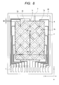
- FIG. 8 is a plan view for showing an electrode pattern of the capacitance-type touch panel in the display device having a touch panel according to the embodiment of the present invention.
- FIG. 9 is a diagram for explaining a shield electrode in the display device having a touch panel according to the embodiment of the present invention
- FIG. 10 is a cross-sectional view for showing a cross-sectional structure taken along the line A-A′ of FIG. 8 ;
- FIG. 11 is a cross-sectional view for showing a cross-sectional structure taken along the line B-B′ of FIG. 8 ;
- FIG. 12 is a cross-sectional view for showing a cross-sectional structure of another example of the capacitance-type touch panel shown in FIG. 8 and for showing a cross-sectional structure taken along the line A-A′ of FIG. 8 ;
- FIG. 13 is a cross-sectional view for showing a cross-sectional structure of still another example of the capacitance-type touch panel shown in FIG. 8 and for showing a cross-sectional structure taken along the line B-B′ of FIG. 8 ;
- FIG. 14 is a cross-sectional view for showing a cross-sectional structure of still another example of the capacitance-type touch panel shown in FIG. 8 and for showing a cross-sectional structure taken along the line A-A′ of FIG. 8 ;
- FIG. 15 is a cross-sectional view for showing a cross-sectional structure of still another example of the capacitance-type touch panel shown in FIG. 8 and for showing a cross-sectional structure taken along the line B-B′ of FIG. 8 .
- FIG. 1 is a diagram for showing an outline configuration of a display device having a touch panel according to the embodiment of the present invention.
- the reference numeral 400 denotes a touch panel .
- the touch panel 400 includes X-electrodes and Y-electrodes for detection of capacity.
- X 1 to X 4 X-electrodes
- Y 1 to Y 4 Y-electrodes
- the touch panel 400 is installed on a front surface of a display device 600 .
- the touch panel 400 is desirably high in the light transmission rate.
- the X-electrodes and the Y-electrodes of the touch panel 400 are coupled to a capacity detector 102 though detection wirings 201 .
- the capacity detector 102 is controlled by a detection controlling signal 202 output from a controller 103 .
- the X-electrodes X 1 to X 4 used as transmission electrodes (driving electrodes) sequentially apply pulses and the Y-electrodes Y 1 to Y 4 are used as reception electrodes to measure capacity between the electrodes at each intersecting point of the electrodes.
- a capacity detecting signal 203 that is changed depending on the capacitance value of each intersecting point between the electrodes is output to the controller 103 .
- a memory 4 records therein a reference value 41 , a measured value 42 , and a signal value 43 for each intersecting point between the electrodes (X-electrodes and Y-electrodes) and stores therein a touch status management table 44 .
- the reference value 41 , the measured value 42 , and the signal value 43 are two-dimensional sequence data in which the number of X-electrodes is the number of elements in the horizontal direction and the number of Y-electrodes is the number of elements in the vertical direction.
- the reference value 41 is data for recording the measured value 42 in a non-touched status.
- the signal value 43 is data calculated on the basis of the measured value 42 in the touch detection process.
- the touch status management table 44 is a table for storing touch coordinates and the like as touch detection results.
- the controller 103 calculates each capacity between the electrodes using the capacity detecting signal 203 of each electrode, and obtains input coordinates by computation using each capacity between the electrodes.
- the controller 103 transfers the input coordinates to a system controller 104 using an I/F signal 204 .
- the system controller 104 If the input coordinates are transferred from the touch panel 400 by a touch operation, the system controller 104 generates a display image in accordance with the touch operation to be transferred to a display controlling circuit 105 as a display controlling signal 205 .
- the display controlling circuit 105 generates a display signal 206 in accordance with the display image transferred by the display controlling signal 205 , and displays the image on the display device 600 .
- FIG. 2 is a cross-sectional view of main parts for explaining the display device having a touch panel according to the embodiment of the present invention, and is also a diagram for explaining a multilayer structure in which a touch panel and a front panel are laminated on a display panel.
- any display panel may be used as long as a touch panel can be used.
- the display panel is not limited to a liquid crystal display panel, but may be a display panel using organic light-emitting diode elements or surface-conduction electron-emitter elements, or an organic EL display panel.
- the display device 600 of the embodiment includes a liquid crystal display panel 100 , the capacitance-type touch panel 400 that is arranged on the surface of the liquid crystal display panel 100 on the viewer side, and a backlight 700 that is arranged under the surface of the liquid crystal display panel 100 on the side opposite to the viewer side.
- the liquid crystal display panel 100 for example, an IPS-type, a TN-type, or a VA-type liquid crystal display panel is used.
- the liquid crystal display panel 100 is formed by attaching two substrates 620 and 630 that are opposed to each other, and polarization plates 601 and 602 are provided outside the two substrates.
- liquid crystal display panel 100 is attached to the touch panel 400 using a first adhesive 501 made of a resin adhesive film.
- a front panel (also referred to as a front-face protection plate or a front window) 12 made of acrylic resin is attached outside the touch panel 400 using second adhesives 502 made of resin adhesive films.
- FIG. 3 shows a state in which a flexible print substrate 70 is coupled to the touch panel 400 . It should be noted that a shielding conductive film 38 , to be described later, is not illustrated in FIG. 3 .
- a driving circuit 150 is mounted on the flexible print substrate 70 , and a signal output from the driving circuit 150 is supplied to the touch panel 400 via the flexible print substrate 70 . Detection of an input position and the like are controlled by the driving circuit 150 .
- the memory 4 , the capacity detector 102 , and the controller 103 shown in FIG. 1 are provided in the driving circuit.
- the signal output from the driving circuit 150 is supplied to wirings 73 on the flexible print substrate 70 .
- Through-holes 78 are formed at the wirings 73 , and crossed wirings 77 on the back face are electrically coupled to the wirings 73 via the through-holes 78 .
- Each of the crossed wirings 77 intersects with the plural wirings 73 , and is coupled to the wirings 73 again via the through-hole 78 formed at the other end.
- Each of the crossed wirings 77 is orthogonal to the wirings 73 so as to minimize overlapped areas.
- the reference numerals 6 and 7 denote wirings and connecting terminals, respectively, in FIG. 3 .
- AR denotes an effective touch area that is a touch detectable area when the touch panel 400 is touched with a finger, a conductive pen, or an insulating pen.
- a spacer 30 is inserted between the substrate 620 and the touch panel 400 in FIG. 2 .
- a hybrid structure in which the touch panel 400 and the front panel 12 are combined with the liquid crystal display panel 100 has a problem that the substrate 620 of the liquid crystal display panel 100 is low in glass strength.
- An area of the substrate 620 where a liquid crystal driving circuit 50 is mounted protrudes relative to the other substrate 630 to be formed as one substrate.
- the substrate 620 is possibly damaged at the area where the liquid crystal driving circuit 50 is mounted.
- the spacer 30 is inserted between the substrate 620 and touch panel 400 to improve the strength.
- a protective sheet 510 is provided on a front surface of the front panel 12 in FIG. 2 to prevent the front panel 12 from being scratched by a pen and the like.
- the liquid crystal display device includes the liquid crystal display panel 100 , the liquid crystal driving circuit 50 , a flexible print substrate 72 , and the backlight 700 .
- the liquid crystal driving circuit 50 is provided at one side of the liquid crystal display panel 100 , and supplies various signals to the liquid crystal display panel 100 .
- the flexible print substrate 72 is electrically coupled to the liquid crystal driving circuit 50 , so that signals are supplied from outside.
- the liquid crystal display panel 100 is configured in such a manner that: the substrate 620 (hereinafter, also referred to as a TFT substrate) on which thin-film transistors, pixel electrodes, opposed electrodes (common electrodes) and the like are formed is laminated on the substrate 630 (hereinafter, also referred to as a filter substrate) on which color filters and the like are formed with a predetermined interval; the both substrates are attached to each other through frame-like seal members (not shown) provided near edge portions of the both substrates; liquid crystal compositions are enclosed and sealed inside the sealed members; the polarization plates 601 and 602 are attached outside the both substrates; and the flexible print substrate 72 is coupled to the TFT substrate 620 .
- the substrate 620 hereinafter, also referred to as a TFT substrate
- the substrate 630 hereinafter, also referred to as a filter substrate
- the both substrates are attached to each other through frame-like seal members (not shown) provided near edge portions of the both substrates
- liquid crystal compositions are
- the embodiment can be similarly applied to a so-called transverse electric field-type liquid crystal display panel in which opposed electrodes are provided on the TFT substrate 620 and a so-called vertical electric field-type liquid crystal display panel in which opposed electrodes are provided on the filter substrate 630 .
- FIG. 4 is a cross-sectional view for showing an adhesion state between the front panel 12 and the capacitance-type touch panel 400 in a conventional display device having a touch panel.
- the reference numeral 12 denotes the front panel; 15 , a touch panel substrate; 34 denotes an interval layer (air layer) between the front panel 12 and the capacitance-type touch panel 400 ; 35 denotes wiring portions at which the wirings 6 are formed; 36 denotes an electrode (X-electrode and Y-electrode) layer; and 502 denotes the second adhesives made of resin adhesive films.
- the interval layer (air layer) having a thickness of 0.2 mm to 0.4 mm is provided between the front panel 12 and the capacitance-type touch panel.
- the wiring portions 35 at which the wirings 6 for coupling the electrodes (X-electrodes and Y-electrodes) in the effective touch area AR to the connecting terminals 7 are arranged are provided at peripheral portions of the capacitance-type touch panel 400 .
- the second adhesives 502 are provided on the wiring portions 35 , and the wiring portions 35 are required to be as narrow as possible because the wiring portions 35 become ineffective areas in touch detection. Therefore, intervals between the second adhesives 502 and the effective touch area AR are narrow in general.
- FIG. 5 is a graph for explaining a principle of a touch detection method in the conventional display device having a touch panel.
- the horizontal axis represents time (t) and the vertical axis represents a measured value (a digital value obtained by converting a measurement result of the capacitance value between the electrodes from analog to digital).
- L 1 and L 2 represent a measured value and a reference value, respectively, in FIG. 5 .
- an area indicated by an arrow B from time t 0 in FIG. 5 represents an area detected as touched.
- pulses are sequentially applied from the X-electrodes X 1 to X 4 , and the reference value L 2 is calculated from the measured value L 1 of the capacity between the electrodes at each intersecting point of the electrodes received by the Y-electrodes Y 1 to Y 4 , so that whether or not the panel has been touched is detected.
- This scheme prevents false operations even if the capacity between the electrodes at each intersecting point of the electrodes is changed due to temperature and humidity.
- the reference value L 2 it is determined in each scan whether the measured value L 1 of the capacity between the electrodes at each intersecting point of the electrodes is larger (obviously, smaller than a threshold value Sth) than the current reference value, or smaller.
- a counter for counting up the reference value is up.
- the reference value is updated to a value larger than the current reference value.
- a counter for counting down the reference value is up.
- the reference value is updated to a value smaller than the current reference value.
- the capacity between the electrodes at the touched portion is rapidly increased.
- the measured value L 1 of the capacity between the electrodes at the touched portion exceeds the threshold value (Sth) set by the reference value L 2 to be detected as touched, and the update of the reference value L 2 is stopped.
- the interval layer 34 becomes narrow at the touched portion.
- the peripheral portions of the touch panel and the front panel 12 are attached to each other using the second adhesives 502 , changes of the interval layer 34 are limited.
- the interval layer 34 becomes wide at the peripheral portions to cause false operations in some cases.
- FIG. 6 is a graph for explaining false operations at the peripheral portions in the conventional display device having a touch panel. It should be noted that the horizontal axis represents time (t) and the vertical axis represents a measured value (a digital value obtained by converting the measured value of the capacitance value between the electrodes from analog to digital) in FIG. 6 . Further, an area C in FIG. 6 represents a period in which the interval layer 34 becomes wide.
- the capacitance value between the electrodes appears to be reduced when viewed from the driving circuit 150 , and the measured value L 1 is decreased.
- the reference value L 2 is accordingly decreased.
- the measured value L 1 is rapidly increased to exceed the threshold value Sth set by the reference value L 2 , and the update of the reference value L 2 is stopped, resulting in false recognition as touched.
- peripheral portions of the front panel 12 are not touched with a finger of a person, the peripheral portions of the front panel 12 are always recognized as touched.
- the shielding conductive film 38 to which predetermined electric potential is supplied is provided on the top surface of the touch panel 400 near the second adhesives 502 of the touch panel 400 so as to surround the effective touch area of the capacitance-type touch panel 400 as shown in FIG. 7 and FIG. 8 in the embodiment.
- the capacitance value between the electrodes at a portion of the shielding conductive film 38 becomes constant. Even if the thickness of the interval layer 34 is changed, the measured value of the capacity between the electrodes is not reacted and false operations can be prevented.
- FIG. 7 is a cross-sectional view for showing an adhesion state between the front panel 12 and the capacitance-type touch panel 400 in the display device having a touch panel according to the embodiment of the present invention
- FIG. 8 is a diagram for showing an electrode pattern of the capacitance-type touch panel 400 according to the embodiment of the present invention.
- the reference numerals 37 and 38 denote a protective layer and a shielding conductive film (for example, a grounded transparent conductive film (ITO)), respectively.
- the shielding conductive film 38 is coupled to, for example, one of the connecting terminals 7 of the flexible print substrate 72 , and ground potential is supplied to the shielding conductive film 38 .
- the shielding conductive film 38 overlaps the peripheral portions of the effective touch area AR in planar view.
- a slit 8 is formed in the shielding conductive film 38 and the shielding conductive film 38 is formed in a loop shape to be prevented from functioning as an antenna.
- end portions of the shielding conductive film 38 where the peripheral portions of the effective touch area AR of the touch panel 400 overlap are desirably positioned in an area (area W 1 shown in FIG. 8 ) of 3 mm to 5 mm at the peripheral portions of the effective touch area AR of the touch panel 400 in planar view.
- the end portions of the shielding conductive film 38 where the peripheral portions of the effective touch area AR of the touch panel 400 overlap are desirably positioned within a range (range W 2 shown in FIG. 7 ) of 3 mm to 5 mm from the second adhesives 502 in planar view.
- FIG. 9 is a diagram for explaining a connection state between the wirings 6 and the electrodes (X-electrodes and Y-electrodes).
- the wiring 6 is configured using a transparent conductive film (ITO) configuring electrodes (X-electrodes and Y-electrodes) and a metal film formed on the transparent conductive film (ITO).
- ITO transparent conductive film
- the end portions of the shielding conductive film 38 where the peripheral portions of the effective touch area AR of the touch panel 400 overlap are desirably positioned within a range (range W 3 shown in FIG. 9 ) of 3 mm to 5 mm from the connection position between the transparent conductive film (ITO) and the metal film in planar view.
- FIG. 10 and FIG. 11 are cross-sectional views for showing a cross-sectional structure of the capacitance-type touch panel shown in FIG. 8 .
- FIG. 10 is a cross-sectional view for showing a cross-sectional structure taken along the line A-A′ of FIG. 8
- FIG. 11 is a cross-sectional view for showing a cross-sectional structure taken along the line B-B′ of FIG. 8 .
- the capacitance-type touch panel shown in FIG. 8 includes plural X-electrodes that extend in a second direction (for example, Y-direction) and are arranged in parallel at predetermined arrangement pitches in a first direction (for example, X-direction) intersecting with the second direction on the surface of the touch panel substrate 15 on the viewer side, and plural Y-electrodes that extend in the first direction while intersecting with the plural X-electrodes and are arranged in parallel at predetermined arrangement pitches in the second direction.
- a transparent insulating substrate such as glass is used as the touch panel substrate 15 .
- Each of the plural X-electrodes are formed in an electrode pattern in which thin line portions 1 a and pad portions 1 b whose widths are larger than those of the thin line portions la are alternately arranged in the second direction.
- Each of the plural Y-electrodes are formed in an electrode pattern in which thin line portions 2 a and pad portions 2 b whose widths are larger than those of the thin line portions 2 a are alternately arranged in the first direction.
- An area where the plural Y-electrodes and X-electrodes are arranged serves as the effective touch area AR, and plural wirings 6 that are electrically coupled to the plural Y-electrodes and X-electrodes are arranged around the effective touch area AR as shown in FIG. 8 .
- the plural X-electrodes are arranged on the surface of the touch panel substrate 15 on the viewer side.
- the pad portions 2 b of the plural Y-electrodes are formed separately from the X-electrodes on the surface of the touch panel substrate 15 on the viewer side.
- the thin line portions 2 a of the plural Y-electrodes are arranged on an insulating film (PAS 1 ) formed on the surface of the touch panel substrate 15 on the viewer side. It should be noted that the thin line portions 2 a of the plural Y-electrodes are covered with a protective film (PAS 2 ) formed thereon.
- the protective film (PAS 2 ) can be used as a protective layer 37 .
- Each of the thin line portions 2 a of the Y-electrodes intersects with each of the thin line portions la of the X-electrodes in planar view.
- Each of the thin line portions 2 a is electrically coupled to two adjacent pad portions 2 b sandwiching the thin line portion 2 a through a contact hole 12 a formed at the insulating film (PAS 1 ) as an interlayer insulating film between the thin line portion 2 a of the Y-electrode and the thin line portion 1 a of the X-electrode.
- PAS 1 insulating film
- each pad portion 2 b of the Y-electrodes is arranged between two adjacent thin line portions 1 a of the X-electrodes and each pad portion 1 b of the X-electrodes is arranged between two adjacent thin line portions 2 a of the Y-electrodes.
- the plural X-electrodes and Y-electrodes are made of transparent conductive material such as Indium Tin Oxide (ITO) with high permeability.
- the wiring 6 is configured using, for example, a transparent conductive layer of a lower layer made of transparent conductive material such as Indium Tin Oxide (ITO) and a metal layer of an upper layer made of silver alloy material.
- FIG. 12 and FIG. 13 are cross-sectional views for showing a cross-sectional structure of another example of the capacitance-type touch panel shown in FIG. 8 .
- FIG. 12 is a cross-sectional view for showing a cross-sectional structure taken along the line A-A′ of FIG. 8
- FIG. 13 is a cross-sectional view for showing a cross-sectional structure taken along the line B-B′ of FIG. 8 .
- the thin line portions 2 a of the plural Y-electrodes are arranged on the surface of the touch panel substrate 15 on the viewer side, and the thin line portions la of the plural X-electrodes and the pad portions 2 b of the plural Y-electrodes are formed on the insulating film (PAS 1 ).
- the thin line portions 1 a and the pad portions 1 b of the plural X-electrodes and the pad portions 2 b of the plural Y-electrodes are covered with the protective film (PAS 2 ) formed thereon.
- the protective film (PAS 2 ) can be used as the protective layer 37 .
- Each of the thin line portions 2 a of the Y-electrodes intersects with each of the thin line portions la of the X-electrodes in planar view.
- Each of the thin line portions 2 a is electrically coupled to two adjacent pad portions 2 b sandwiching the thin line portion 2 a through the contact hole 12 a formed at the insulating film (PAS 1 ) as an interlayer insulating film between the thin line portion 2 a of the Y-electrode and the thin line portion 1 a of the X-electrode.
- PAS 1 insulating film
- each pad portion 2 b of the Y-electrodes is arranged between two adjacent thin line portions 1 a of the X-electrodes and each pad portion 1 b of the X-electrodes is arranged between two adjacent thin line portions 2 a of the Y-electrodes.
- the plural X-electrodes and Y-electrodes are made of transparent conductive material such as Indium Tin Oxide (ITO) with high permeability.
- the wiring 6 is configured using, for example, a transparent conductive layer of a lower layer made of transparent conductive material such as Indium Tin Oxide (ITO) and a metal layer of an upper layer made of silver alloy material.
- FIG. 14 and FIG. 15 are cross-sectional views for showing a cross-sectional structure of still another example of the capacitance-type touch panel shown in FIG. 8 .
- FIG. 14 is a cross-sectional view for showing a cross-sectional structure taken along the line A-A′ of FIG. 8
- FIG. 15 is a cross-sectional view for showing a cross-sectional structure taken along the line B-B′ of FIG. 8 .
- the thin line portions 1 a and the pad portions 1 a of the plural X-electrodes are arranged on the surface of the touch panel substrate 15 on the viewer side, and the thin line portions 2 a and the pad portions 2 b of the plural Y-electrodes are formed on the insulating film (PAS 1 ).
- the thin line portions 2 a and the pad portions 2 b of the plural Y-electrodes are covered with the protective film (PAS 2 ) formed thereon.
- the protective film (PAS 2 ) can be used as the protective layer 37 .
- the X-electrodes and the Y-electrodes are formed on the different layers, and the thin line portions 2 a of the Y-electrodes intersect with the thin line portions 1 a of the X-electrodes in planar view.
- each pad portion 2 b of the Y-electrodes is arranged between two adjacent thin line portions 1 a of the X-electrodes and each pad portion 1 b of the X-electrodes is arranged between two adjacent thin line portions 2 a of the Y-electrodes.
- the plural X-electrodes and Y-electrodes are made of transparent conductive material such as Indium Tin Oxide (ITO) with high permeability.
- the wiring 6 is configured using, for example, a transparent conductive layer of a lower layer made of transparent conductive material such as Indium Tin Oxide (ITO) and a metal layer of an upper layer made of silver alloy material.
Landscapes
- Engineering & Computer Science (AREA)
- General Engineering & Computer Science (AREA)
- Theoretical Computer Science (AREA)
- Human Computer Interaction (AREA)
- Physics & Mathematics (AREA)
- General Physics & Mathematics (AREA)
- Position Input By Displaying (AREA)
Abstract
Description
Claims (7)
Applications Claiming Priority (2)
| Application Number | Priority Date | Filing Date | Title |
|---|---|---|---|
| JP2010-231091 | 2010-10-14 | ||
| JP2010231091A JP2012084025A (en) | 2010-10-14 | 2010-10-14 | Display device with touch panel |
Publications (2)
| Publication Number | Publication Date |
|---|---|
| US20120092292A1 US20120092292A1 (en) | 2012-04-19 |
| US8736576B2 true US8736576B2 (en) | 2014-05-27 |
Family
ID=45933731
Family Applications (1)
| Application Number | Title | Priority Date | Filing Date |
|---|---|---|---|
| US13/270,294 Active 2032-07-09 US8736576B2 (en) | 2010-10-14 | 2011-10-11 | Display device having touch panel |
Country Status (2)
| Country | Link |
|---|---|
| US (1) | US8736576B2 (en) |
| JP (1) | JP2012084025A (en) |
Cited By (3)
| Publication number | Priority date | Publication date | Assignee | Title |
|---|---|---|---|---|
| US20130093697A1 (en) * | 2011-10-18 | 2013-04-18 | Wei-Hao Sun | Touch panel display and assembly process thereof |
| US20140043248A1 (en) * | 2012-08-13 | 2014-02-13 | Chih-Shan Yeh | Touch panel structure, touch and display panel structure, and integrated touch display panel structure having antenna pattern and method of forming touch panel having antenna pattern |
| US20150002761A1 (en) * | 2012-01-18 | 2015-01-01 | Kyocera Corporation | Input apparatus, display apparatus, and electronic apparatus |
Families Citing this family (14)
| Publication number | Priority date | Publication date | Assignee | Title |
|---|---|---|---|---|
| JP2014026199A (en) | 2012-07-30 | 2014-02-06 | Japan Display Inc | Liquid crystal display device |
| KR102017155B1 (en) * | 2012-11-01 | 2019-09-03 | 삼성디스플레이 주식회사 | Touch screen panel and method for manufacturing the same |
| TWI478024B (en) * | 2013-05-31 | 2015-03-21 | Eturbo Touch Technology Inc | Touch panel and the touch panel making method |
| KR101452302B1 (en) | 2013-07-29 | 2014-10-22 | 주식회사 하이딥 | Touch sensor panel |
| KR101681305B1 (en) * | 2014-08-01 | 2016-12-02 | 주식회사 하이딥 | Touch input device |
| KR101712346B1 (en) | 2014-09-19 | 2017-03-22 | 주식회사 하이딥 | Touch input device |
| KR102377905B1 (en) * | 2014-04-08 | 2022-03-23 | 삼성디스플레이 주식회사 | Flat panel display |
| JP6527343B2 (en) | 2014-08-01 | 2019-06-05 | 株式会社 ハイディープHiDeep Inc. | Touch input device |
| JP6521813B2 (en) | 2015-09-18 | 2019-05-29 | 株式会社ジャパンディスプレイ | Display device with sensor and sensor device |
| JP2017107439A (en) * | 2015-12-10 | 2017-06-15 | 凸版印刷株式会社 | Film sensor module and flexible substrate for film sensor module |
| JP6710531B2 (en) | 2016-02-03 | 2020-06-17 | 株式会社ジャパンディスプレイ | Display device with sensor and sensor device |
| KR102633061B1 (en) * | 2016-09-23 | 2024-02-06 | 삼성디스플레이 주식회사 | Display device and method for manufacturing the same |
| US10241631B2 (en) * | 2017-03-21 | 2019-03-26 | Intel Corporation | Hybrid display integratable antennas using touch sensor trace and edge discontinuity structures |
| JP6903476B2 (en) * | 2017-04-20 | 2021-07-14 | 株式会社ジャパンディスプレイ | Display device |
Citations (5)
| Publication number | Priority date | Publication date | Assignee | Title |
|---|---|---|---|---|
| JP2003511799A (en) | 1999-10-08 | 2003-03-25 | シナプティクス インコーポレイテッド | Flexible and transparent contact detection system for electronic devices |
| US20110069036A1 (en) * | 2009-09-18 | 2011-03-24 | Hitachi Displays, Ltd. | Display device |
| US20110285661A1 (en) * | 2010-05-18 | 2011-11-24 | Steven Porter Hotelling | Periphery Conductive Element for Touch Screen |
| US8194044B2 (en) * | 2003-12-15 | 2012-06-05 | 3M Innovative Properties Company | Wiring harness and touch sensor incorporating same |
| US8330734B2 (en) * | 2008-09-05 | 2012-12-11 | Hitachi Displays, Ltd. | Liquid crystal display device |
-
2010
- 2010-10-14 JP JP2010231091A patent/JP2012084025A/en active Pending
-
2011
- 2011-10-11 US US13/270,294 patent/US8736576B2/en active Active
Patent Citations (6)
| Publication number | Priority date | Publication date | Assignee | Title |
|---|---|---|---|---|
| JP2003511799A (en) | 1999-10-08 | 2003-03-25 | シナプティクス インコーポレイテッド | Flexible and transparent contact detection system for electronic devices |
| US7030860B1 (en) | 1999-10-08 | 2006-04-18 | Synaptics Incorporated | Flexible transparent touch sensing system for electronic devices |
| US8194044B2 (en) * | 2003-12-15 | 2012-06-05 | 3M Innovative Properties Company | Wiring harness and touch sensor incorporating same |
| US8330734B2 (en) * | 2008-09-05 | 2012-12-11 | Hitachi Displays, Ltd. | Liquid crystal display device |
| US20110069036A1 (en) * | 2009-09-18 | 2011-03-24 | Hitachi Displays, Ltd. | Display device |
| US20110285661A1 (en) * | 2010-05-18 | 2011-11-24 | Steven Porter Hotelling | Periphery Conductive Element for Touch Screen |
Cited By (5)
| Publication number | Priority date | Publication date | Assignee | Title |
|---|---|---|---|---|
| US20130093697A1 (en) * | 2011-10-18 | 2013-04-18 | Wei-Hao Sun | Touch panel display and assembly process thereof |
| US20150002761A1 (en) * | 2012-01-18 | 2015-01-01 | Kyocera Corporation | Input apparatus, display apparatus, and electronic apparatus |
| US10159146B2 (en) * | 2012-01-18 | 2018-12-18 | Kyocera Corporation | Input apparatus, display apparatus, and electronic apparatus |
| US20140043248A1 (en) * | 2012-08-13 | 2014-02-13 | Chih-Shan Yeh | Touch panel structure, touch and display panel structure, and integrated touch display panel structure having antenna pattern and method of forming touch panel having antenna pattern |
| US8933902B2 (en) * | 2012-08-13 | 2015-01-13 | Htc Corporation | Touch panel structure, touch and display panel structure, and integrated touch display panel structure having antenna pattern and method of forming touch panel having antenna pattern |
Also Published As
| Publication number | Publication date |
|---|---|
| US20120092292A1 (en) | 2012-04-19 |
| JP2012084025A (en) | 2012-04-26 |
Similar Documents
| Publication | Publication Date | Title |
|---|---|---|
| US8736576B2 (en) | Display device having touch panel | |
| KR101386327B1 (en) | Display device equipped with touch panel | |
| EP3037937B1 (en) | Touch input device | |
| KR100837738B1 (en) | Electronic device and touch panel arrangement method of the same | |
| KR101613379B1 (en) | Touch sensitive displays | |
| JP5178817B2 (en) | Display device, electronic device including the same, and touch panel | |
| CN102436323B (en) | Display device associated with touch panel and producing method thereof | |
| JP5337061B2 (en) | Touch panel and display device including the same | |
| US8994668B2 (en) | Electrooptic device having input function | |
| US8390575B2 (en) | Touch-sensitive liquid crystal display panel with built-in touch mechanism and method for driving same | |
| US20110069036A1 (en) | Display device | |
| US20110134075A1 (en) | Touch panel, display, and electronic device | |
| EP2575017A1 (en) | Touch sensing apparatus and method of manufacturing the same | |
| US20150029148A1 (en) | Capacitive in-cell touch screen panel and display device | |
| KR101507235B1 (en) | Touch sensor integrated type display device | |
| KR20160063540A (en) | Display device including touch sensor and driving method thereof | |
| KR20140134619A (en) | Electronic component, touch panel and liquid crystal display device using the same | |
| JP2022033524A (en) | Touch panel and display device | |
| CN114270300B (en) | Touch panel device | |
| US20110115725A1 (en) | Touch Panel and Display Device Including the Same and Touch Position Detection Method of Touch Panel | |
| KR101859469B1 (en) | Display device and manufacturing method thereof | |
| US11847288B2 (en) | Touch panel and display apparatus including touch panel | |
| KR20080054736A (en) | Touch screen panel | |
| KR20210069210A (en) | Touch display device and driving circuit module |
Legal Events
| Date | Code | Title | Description |
|---|---|---|---|
| AS | Assignment |
Owner name: PANASONIC LIQUID CRYSTAL DISPLAY CO., LTD., JAPAN Free format text: ASSIGNMENT OF ASSIGNORS INTEREST;ASSIGNOR:HAYAKAWA, KOUJI;REEL/FRAME:027040/0278 Effective date: 20110913 Owner name: HITACHI DISPLAYS, LTD., JAPAN Free format text: ASSIGNMENT OF ASSIGNORS INTEREST;ASSIGNOR:HAYAKAWA, KOUJI;REEL/FRAME:027040/0278 Effective date: 20110913 |
|
| AS | Assignment |
Owner name: JAPAN DISPLAY EAST, INC., JAPAN Free format text: CHANGE OF NAME;ASSIGNOR:HITACHI DISPLAYS, LTD.;REEL/FRAME:031848/0902 Effective date: 20120401 Owner name: JAPAN DISPLAY INC., JAPAN Free format text: CHANGE OF NAME;ASSIGNOR:JAPAN DISPLAY EAST, INC.;REEL/FRAME:031865/0489 Effective date: 20130401 |
|
| STCF | Information on status: patent grant |
Free format text: PATENTED CASE |
|
| MAFP | Maintenance fee payment |
Free format text: PAYMENT OF MAINTENANCE FEE, 4TH YEAR, LARGE ENTITY (ORIGINAL EVENT CODE: M1551) Year of fee payment: 4 |
|
| MAFP | Maintenance fee payment |
Free format text: PAYMENT OF MAINTENANCE FEE, 8TH YEAR, LARGE ENTITY (ORIGINAL EVENT CODE: M1552); ENTITY STATUS OF PATENT OWNER: LARGE ENTITY Year of fee payment: 8 |
|
| AS | Assignment |
Owner name: PANASONIC INTELLECTUAL PROPERTY CORPORATION OF AMERICA, CALIFORNIA Free format text: NUNC PRO TUNC ASSIGNMENT;ASSIGNOR:PANASONIC LIQUID CRYSTAL DISPLAY CO., LTD.;REEL/FRAME:065615/0327 Effective date: 20230828 |
|
| AS | Assignment |
Owner name: PANELTOUCH TECHNOLOGIES LLC, TEXAS Free format text: ASSIGNMENT OF ASSIGNORS INTEREST;ASSIGNORS:PANASONIC INTELLECTUAL PROPERTY CORPORATION OF AMERICA;JAPAN DISPLAY INC.;REEL/FRAME:067245/0560 Effective date: 20240322 |