US8729937B2 - Coarse lock detector - Google Patents
Coarse lock detector Download PDFInfo
- Publication number
- US8729937B2 US8729937B2 US13/398,532 US201213398532A US8729937B2 US 8729937 B2 US8729937 B2 US 8729937B2 US 201213398532 A US201213398532 A US 201213398532A US 8729937 B2 US8729937 B2 US 8729937B2
- Authority
- US
- United States
- Prior art keywords
- detection cell
- frequency detection
- detection
- lock detector
- cells
- Prior art date
- Legal status (The legal status is an assumption and is not a legal conclusion. Google has not performed a legal analysis and makes no representation as to the accuracy of the status listed.)
- Active
Links
Images


Classifications
-
- H—ELECTRICITY
- H03—ELECTRONIC CIRCUITRY
- H03L—AUTOMATIC CONTROL, STARTING, SYNCHRONISATION OR STABILISATION OF GENERATORS OF ELECTRONIC OSCILLATIONS OR PULSES
- H03L7/00—Automatic control of frequency or phase; Synchronisation
- H03L7/06—Automatic control of frequency or phase; Synchronisation using a reference signal applied to a frequency- or phase-locked loop
- H03L7/08—Details of the phase-locked loop
- H03L7/085—Details of the phase-locked loop concerning mainly the frequency- or phase-detection arrangement including the filtering or amplification of its output signal
- H03L7/095—Details of the phase-locked loop concerning mainly the frequency- or phase-detection arrangement including the filtering or amplification of its output signal using a lock detector
-
- H—ELECTRICITY
- H03—ELECTRONIC CIRCUITRY
- H03L—AUTOMATIC CONTROL, STARTING, SYNCHRONISATION OR STABILISATION OF GENERATORS OF ELECTRONIC OSCILLATIONS OR PULSES
- H03L7/00—Automatic control of frequency or phase; Synchronisation
- H03L7/06—Automatic control of frequency or phase; Synchronisation using a reference signal applied to a frequency- or phase-locked loop
- H03L7/08—Details of the phase-locked loop
- H03L7/081—Details of the phase-locked loop provided with an additional controlled phase shifter
- H03L7/0812—Details of the phase-locked loop provided with an additional controlled phase shifter and where no voltage or current controlled oscillator is used
-
- H—ELECTRICITY
- H03—ELECTRONIC CIRCUITRY
- H03L—AUTOMATIC CONTROL, STARTING, SYNCHRONISATION OR STABILISATION OF GENERATORS OF ELECTRONIC OSCILLATIONS OR PULSES
- H03L7/00—Automatic control of frequency or phase; Synchronisation
- H03L7/06—Automatic control of frequency or phase; Synchronisation using a reference signal applied to a frequency- or phase-locked loop
- H03L7/08—Details of the phase-locked loop
- H03L7/10—Details of the phase-locked loop for assuring initial synchronisation or for broadening the capture range
- H03L7/101—Details of the phase-locked loop for assuring initial synchronisation or for broadening the capture range using an additional control signal to the controlled loop oscillator derived from a signal generated in the loop
Definitions
- the described technology relates to a delayed locked loop (DLL), and more particularly, to a coarse lock detector for a DLL.
- DLL delayed locked loop
- a semiconductor integrated circuit operates using clocks to control its operating speed.
- the semiconductor integrated circuit includes a clock buffer to buffer clocks input from an external source.
- the semiconductor integrated circuit uses a delayed locked loop (DLL) circuit or a phase-locked loop (PLL) circuit to generate and use an internal clock whose phase difference from an external clock has been corrected.
- DLL delayed locked loop
- PLL phase-locked loop
- DLLs are being widely used as zero delay buffers due to their superior jitter characteristics and better stability than PLLs.
- a conventional DLL is likely to have a stuck problem or harmonic lock when operating at high speed.
- FIG. 1 illustrates a structure of a conventional DLL including a coarse lock detector 11 .
- a plurality of delay elements 15 generates a set of multiphase clocks PH[ 1 ] through PH[ 15 ] by incrementally delaying an input reference clock CLK_IN.
- the coarse lock detector 11 receives the input reference clock CLK_IN and a plurality of multiphase clocks.
- some (PH[ 5 ], PH[ 7 ], PH[ 9 ], PH[ 11 ], PH[ 13 ] and PH[ 15 ]) of the multiphase clocks PH[ 1 ] through PH[ 15 ] generated by the delay elements 15 are input to the coarse lock detector 11 .
- the coarse lock detector 11 continuously counts the number of rising edges of the received multiphase clocks and determines whether a phase of the rising edge of each multiphase clock lags behind a phase of the input reference clock CLK_IN, leads the phase of the input reference clock CLK_IN, or is locked to the phase of the input reference clock CLK_IN.
- the coarse lock detector 11 determines that the phase of the rising edge of each multiphase clock lags behind the phase of the input reference clock CLK_IN, phase locking cannot be achieved since a delay chain is too slow. Therefore, the coarse lock detector 11 generates an UP signal indicating a direction in which the frequency should be adjusted. On the other hand, when the coarse lock detector 11 determines that the phase of the rising edge of each multiphase clock leads the phase of the input reference clock CLK_IN, phase locking cannot be achieved since the delay chain is too fast. Therefore, the coarse lock detector 11 generates a DOWN signal. That is, frequency locking can be achieved by adjusting the frequency by using the UP or DOWN signal.
- the stuck problem and harmonic lock are considerations that must be taken into account when designing a DLL and can be solved using a coarse lock detector.
- a conventional coarse lock detector that samples multiphase clocks cannot operate at high speed.
- One inventive aspect is a coarse lock detector including first through p-th detection cells which receive p multiphase clocks generated by incrementally delaying a reference clock.
- the first through p-th detection cells are divided into a first detection cell group of 2m+1 detection cells and a second detection cell group of 2n detection cells, where p is an integer equal to or greater than three, m is an integer equal to or greater than zero when 2m+1 is equal to or smaller than p, and n is an integer equal to or greater than one when 2n is equal to or greater than p.
- a coarse lock detector including first through p-th detection cells which receive p multiphase clocks generated by incrementally delaying a reference clock.
- the first through p-th detection cells are divided into a first detection cell group of 3k+1 detection cells, a second detection cell group of 3s+2 detection cells, and a third detection cell group of 3r detection cells, where p is an integer equal to or greater than four, k is an integer equal to or greater than zero when 3k+1 is equal to or smaller than p, s is an integer equal to or greater than zero when 3s+2 is equal to or smaller than p, and r is an integer equal to or greater than one when 3r is equal to or smaller than p.
- a coarse lock detector including first through P-th detection cells which receive P multiphase clocks generated by incrementally delaying a reference clock.
- the first through P-th detection cells are divided into first through U-th detection cell groups corresponding to the first through P-th multiphase clocks, where each of the first through U-th detection cell groups includes (1 ⁇ A (W) +W)-th through (U ⁇ A (W) +W)-th detection cells, where U is an integer equal to or greater than four, P is an integer greater than U, W is an integer that satisfies 1 ⁇ W ⁇ U, and A (W) is an integer equal to or greater than zero when each of (1 ⁇ A (W) +W) through (U ⁇ A (W) +W) is equal to or greater than P.
- FIG. 1 illustrates a conventional delayed locked loop (DLL) including a coarse lock detector
- FIG. 2 illustrates a conventional coarse lock detector for a DLL
- FIG. 3 illustrates an example configuration of frequency detection cells in a coarse lock detector for a DLL
- FIG. 4 illustrates another example configuration of frequency detection cells in a coarse lock detector for a DLL
- FIG. 5 shows waveforms of signals when a coarse lock detector operates normally
- FIG. 6 shows waveforms of signals when a stuck problem occurs
- FIG. 7 illustrates the configuration of frequency detection cells in a coarse lock detector according to an exemplary embodiment
- FIG. 8 is a waveform diagram illustrating a timing margin that doubled when the coarse lock detector of FIG. 7 was used;
- FIG. 9 illustrates the configuration of frequency detection cells in a coarse lock detector according to another exemplary embodiment
- FIG. 10 shows simulation results obtained when the configuration of the frequency detection cells in the coarse lock detector of FIG. 3 was used
- FIG. 11 shows simulation results obtained when the configuration of the frequency detection cells in the coarse lock detector of FIG. 3 was used
- FIG. 12 shows simulation results obtained when the configuration of the frequency detection cells in the coarse lock detector of FIG. 4 was used
- FIG. 13 shows simulation results obtained when the configuration of the frequency detection cells in the coarse lock detector of FIG. 4 was used
- FIG. 14 shows simulation results obtained when the configuration of frequency detection cells in a coarse lock detector suggested in the present invention was used.
- FIG. 15 shows simulation results obtained when the configuration of the frequency detection cells in an embodiment of a coarse lock detector was used.
- FIG. 2 illustrates a conventional coarse lock detector for a delayed locked loop (DLL).
- FIGS. 3 and 4 illustrate example configurations of frequency detection cells in a coarse lock detector for a DLL.
- FIG. 5 shows waveforms of signals when a coarse lock detector operates normally.
- the conventional coarse lock detector included in the DLL may include a plurality of frequency detection cells 22 which respectively receive a plurality of multiphase clocks generated by incrementally delaying a reference clock REF_CK and process the received multiphase clocks, decision logic 23 , a divider 21 , and two pulse generators 24 and 25 . Certain aspects of the embodiments relate particularly to the configuration of the frequency detection cells.
- the coarse lock detector of FIG. 3 is structured to sample multiphase clocks and then to decide the order of edges of the sampled multiphase clocks.
- the coarse lock detector structured as in FIG. 3 can sample multiphase clocks without any problem.
- the coarse lock detector detects an edge one cycle before an edge of subsequent incoming multiphase clock. Therefore, the DLL may fall into harmonic lock.
- the coarse lock detector of FIG. 4 is structured to sequentially sample multiphase clocks, that is, sample a multiphase clock QA[n ⁇ 1] and then a next multiphase clock QA[n].
- the coarse lock detector structured as in FIG. 4 cannot properly sample multiphase clocks, causing a stuck problem.
- ⁇ t indicates a time interval between multiphase clocks
- each of D 1 through Dn indicates a period of time for which a signal is delayed as it goes through an AND gate and a flip-flop in each frequency detection cell.
- a frequency detection cell shown in the bottom left corner of FIG. 4 receives a signal QA[ 2 ], which is output from a previous frequency detection cell as a result of properly sampling a multiphase clock, as an input signal.
- the frequency detection cell can then sample a multiphase clock PH[ 9 ] using its AND gate. That is, the signal QA[ 2 ] is set before a rising edge of the multiphase clock PH[ 9 ] as shown in FIG. 5 .
- the frequency detection cell and the signals QA[ 2 ] and PH[ 9 ] used here are mere examples. It can be understood that the same should apply to the other frequency detection cells as well to avoid the stuck problem.
- the DLL may fall into harmonic lock when operating at low speed. Ultimately, the DLL cannot operate in a wide frequency range.
- a coarse lock detector using an even/odd sampling method does not sequentially process multiphase clocks, that is, in order of a first frequency detection cell, a second frequency detection cell, a third frequency detection cell, a fourth frequency detection cell, a fifth frequency detection cell, and a sixth frequency detection cell as illustrated in FIG. 4 .
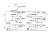
- the coarse lock detector of FIG. 7 processes the multiphase clocks using two groups of frequency detection cells, that is, a first group including the first frequency detection cell, the third frequency detection cell, and the fifth frequency detection cell, and another group including the second frequency detection cell, the fourth frequency detection cell, and the sixth frequency detection cell.
- the time interval ⁇ t doubles as compared to the case of FIG. 4 . That is, dividing frequency detection cells into a group of even-numbered frequency detection cells and a group of odd-numbered frequency detection cells and sampling multiphase clocks using the two groups increases a timing margin, and the increased timing margin prevents the occurrence of the stuck problem in the DLL when operating at high speed.
- a coarse lock detector will now be described in greater detail with reference to FIGS. 7 and 8 .
- FIG. 7 six frequency detection cells 710 through 760 are described as an example. However, this is merely an example used for ease of description. A change in the number of frequency detection cells can be made and is within the scope of the present invention.
- multiphase clocks are input, as input signals, at intervals of two multiphase clocks, such as PH[ 5 ], PH[ 7 ], PH[ 9 ], . . . , PH[ 15 ].
- the present invention is not limited thereto, and those of ordinary skill in that art understand that the interval between the multiphase clocks can be adjusted without departing from the scope of the present invention.
- a total of six frequency detection cells respectively receive one of six multiphase clocks, which are spaced at predetermined intervals, as first input signals.
- Delay elements 15 (see FIG. 1 ) generate the multiphase clocks by delaying a reference clock PH[ 0 ]. If there are a total of p frequency detection cells, an equal number of multiphase clocks that is, p multiphase clocks may be input to the p frequency detection cells as the first input signals. If the coarse lock detector of FIG. 7 includes first through p th frequency detection cells, the first through p th frequency detection cells receive first through p th multiphase clocks as their respective first input signals.
- a divider 705 receives the reference clock PH[ 0 ] and outputs a clock signal whose frequency is half the frequency of the reference clock PH[ 0 ].
- the clock signal whose frequency is half the frequency of the reference clock PH[ 0 ] is input to each of the first through p th multiphase clocks as a third input signal.
- a third frequency detection cell 730 receives an output signal QA[ 1 ] of a first frequency detection cell 710 as its second input signal, performs an AND operation on the signal QA[ 1 ] and a multiphase clock PH[ 9 ] received as a first input signal by using an AND gate 732 , and sends the result of the AND operation to a flip-flop 734 .
- a signal QA[ 3 ] output from the flip-flop 734 is used as a second input signal of a fifth frequency detection cell 750 .
- the fifth frequency detection cell 750 receives the output signal QA[ 3 ] of the third frequency detection cell 730 as its second input signal, performs an AND operation on the signal QA[ 3 ] and a multiphase clock PH[ 13 ] received as a first input signal by using an AND gate 752 , and sends the result of the AND operation to a flip-flop 754 .
- a signal QA[ 5 ] output from the flip-flop 754 may be used as a second input signal of a next frequency detection cell, for example, a seventh frequency detection cell if it exists.
- a fourth frequency detection cell 740 receives an output signal QA[ 2 ] of a second frequency detection cell 720 as its second input signal, performs an AND operation on the signal QA[ 2 ] and a multiphase clock PH[ 11 ] received as a first input signal by using an AND gate 742 , and sends the result of the AND operation to a flip-flop 744 .
- a signal QA[ 4 ] output from the flip-flop 744 is used as a second input signal of a sixth frequency detection cell 760 .
- the sixth frequency detection cell 760 receives the output signal QA[ 4 ] of the fourth frequency detection cell 740 as its second input signal, performs an AND operation on the signal QA[ 4 ] and a multiphase clock PH[ 15 ] received as a first input signal by using an AND gate 762 , and sends the result of the AND operation to a flip-flop 764 .
- a signal QA[ 6 ] output from the flip-flop 764 may be used as a second input signal of a next frequency detection cell, for example, an eighth frequency detection cell if it exists.
- frequency detection cells are divided into a group of even-numbered (2n) frequency detection cells and a group of odd-numbered (2m+1) frequency detection cells to process and sample first through p th multiphase clocks, respectively.
- sampling a multiphase clock denotes generating an output signal which is set in response to a rising edge of each of the first through p th multiphase clocks input respectively to the first through p th frequency detection cells.
- m represents an integer equal to or greater than zero when 2m+1 is equal to or smaller than p
- n is an integer equal to or greater than one when 2n is equal to or smaller than p.
- the second frequency detection cell 720 receives the output signal QA[ 1 ] of the first frequency detection cell 710 as its second input signal. This is because no even-numbered frequency detection cell exists before the second frequency detection cell 720 . Therefore, the second frequency detection cell 720 receives the output signal QA[ 1 ] of the first frequency detection cell 710 as its second input signal, performs an AND operation on the signal QA[ 1 ] and a multiphase clock PH[ 7 ] received as a first input signal by using an AND gate 722 , and sends the result of the AND operation to a flip-flop 724 . The signal QA[ 2 ] output from the flip-flop 724 is used as the second input signal of the fourth frequency detection cell 740 .
- the second frequency detection cell 720 receives and processes the output signal QA[ 1 ] of the first frequency detection cell 710 .
- the value of ⁇ t may be reduced as compared to other cases.
- the first frequency detection cell 710 includes no AND gate, no AND gate delay occurs, thus not causing a great loss in timing margin. That is, a delay time D 1 in the first frequency detection cell 710 is caused only by the flip-flop 714 . Therefore, the delay time D 1 in the first frequency detection cell 710 is shorter than the delay time Dn in the other frequency detection cells.
- the second frequency detection cell 720 receives the output signal QA[ 1 ] of the first frequency detection cell 710 as the input signal and generates the signal QA[ 2 ] using the received signal QA[ 1 ], there is no problem since a loss in timing margin is small.
- the first frequency detection cell 710 does not require an AND gate since it does not need to receive and process an output signal of a previous frequency detection cell. Accordingly, the first frequency detection cell 710 receives only a multiphase clock PH[ 5 ], which is a first multiphase clock, as a first input signal and samples the multiphase clock PH[ 5 ].
- the output signals QA[ 1 ] through QA[p] of the first through p th frequency detection cells are input to decision logic 23 as shown in FIG. 2 .
- the decision logic 23 decides whether the frequency is locked and generates a signal (UP or DOWN) based on the decision result, thereby adjusting the frequency.
- FIG. 9 illustrates a coarse lock detector according to another exemplary embodiment.
- the frequency detection cells are divided into a group of even-numbered frequency detection cells and a group of odd-numbered frequency detection cells to sample multiphase clocks in FIG. 7 .
- they are divided into three groups.
- the basic configuration of each frequency detection cell in FIG. 9 is similar to that of each frequency detection cell in FIG. 7 . Therefore, the following description will focus on differences from FIG. 7 .
- the coarse lock detector processes multiphase clocks using three groups of frequency detection cells, that is, a first group including a first frequency detection cell, a fourth frequency detection cell, and a seventh frequency detection cell, a second group including a second frequency detection cell, a fifth frequency detection cell, and an eighth frequency detection cell, and a third group including a third frequency detection cell, a sixth frequency detection cell, and a ninth frequency detection cell.
- FIG. 9 six frequency detection cells 910 through 960 are illustrated as an example. However, this is merely an example used for ease of illustration in the drawing. A change in the number of frequency detection cells can be made within the scope of the present invention. Therefore, if the coarse lock detector of FIG. 9 further includes seventh through ninth frequency detection cells, multiphase clocks may be processed as discussed above.
- the first through p th frequency detection cells may be divided into a first detection cell group of first, fourth, and seventh frequency detection cells, a second detection cell group of second, fifth, and eighth frequency detection cells, and a third detection cell group of third, sixth, and ninth frequency detection cells to correspond to the first through p th multiphase clocks.
- r represents an integer equal to or greater than one when 3r is equal to or less than p
- k is an integer equal to or greater than zero when 3k+1 is equal to or less than p
- s is an integer equal to or greater than zero when 3s+2 is equal to or less than p.
- a second input signal of a fourth frequency detection cell 940 is an output signal QA[ 1 ] of a first frequency detection cell 910
- a second input signal of a fifth frequency detection cell 950 is an output signal QA[ 2 ] of a second frequency detection signal 920
- a second input signal of a sixth frequency detection cell 960 is an output signal QA[ 3 ] of a third frequency detection cell 930 .
- the value of ⁇ t triples as compared to the case of FIG. 4 .
- a second input signal of the third frequency detection cell 930 is the output signal QA[ 2 ] of the second frequency detection cell 920
- a second input signal of the second frequency detection cell 920 is the output signal QA[ 1 ] of the first frequency detection cell 910 .
- FIGS. 7 and 9 the embodiments in which frequency detection cells are divided into two and three groups are illustrated, respectively.
- the present invention is not limited to these embodiments. Any embodiment in which multiphase clocks are sampled at intervals of multiple multiphase clocks and the sampled multiphase clocks are combined to increase an operating frequency is included in the present invention.
- a coarse lock detector may include first through P th frequency detection cells which respectively receive one of P multiphase clocks generated by incrementally delaying a reference clock and are set in response to rising edges of first through P th multiphase clocks.
- the first through P th frequency detection cells may be divided into a number of groups, e.g., first through U th detection cell groups to respond to the first through P th multiphase clocks.
- the first through P th frequency detection cells may be divided into a 4 ⁇ A (1) +1 group of first, fifth, ninth . . . frequency detection cells, a 4 ⁇ A (2) +2 group of second, sixth, tenth . . . frequency detection cells, a 4 ⁇ A (3) +3 group of third, seventh, eleventh . . . frequency detection cells, and a 4 ⁇ A (4) +4 group of fourth, eighth, twelfth . . . frequency detection cells.
- each of frequency detection cells included in a group uses an output signal of a previous frequency detection cell as its second input signal.
- the fifth frequency detection cell uses an output signal of the first frequency detection cell as its second input signal
- the ninth frequency detection cell uses an output signal of the fifth frequency detection cell as its second input signal (in the case of the 4 ⁇ A (1) +1 group).
- the sixth frequency detection cell uses an output signal of the second frequency detection cell as its second input signal
- the tenth frequency detection cell uses an output of the sixth frequency detection cell as its second input signal (in the case of the 4 ⁇ A (2) +2 group).
- signals of frequency detection cells are also connected as described above.
- Each of second through U th frequency detection cells uses an output signal of an immediately previous frequency detection cell as its second input signal. For example, if U is four, the fourth frequency detection cell uses an output signal of the third frequency detection cell as its second input signal, the third frequency detection cell uses the output signal of the second frequency detection cell as its second input signal, and the second frequency detection cell uses an output signal of the first frequency detection cell as its second input signal.
- FIGS. 10 through 15 Effects that can be achieved when such a coarse lock detector is used is described with reference to FIGS. 10 through 15 .
- simulations were all conducted at 1.2 GHz.
- a condition in which an initial control voltage is zero, that is, a control voltage has a low initial value is a condition that causes harmonic lock
- a condition in which the initial control voltage is VDD, that is, the control voltage has a high initial value is a condition that causes the stuck problem.
- FIGS. 10 and 11 show simulation results obtained when the frequency detection cells in the coarse lock detector of FIG. 3 was used.
- the initial value of the control voltage is set to 0 V
- an interval between multiphase clocks is reduced as the control voltage is increased.
- a simulation was conducted by applying to the coarse lock detector of FIG. 3 the control voltage having a value lower than a value that enables correct locking.
- the coarse lock detector detected an edge one cycle before an edge of a subsequent incoming multiphase clock as shown in FIG. 10 . Therefore, false lock in which a DLL is wrongly detected as being in a coarse lock state occurred. Later, when a phase detector detected that the DLL was not in the coarse lock state, the coarse lock state was broken and recovered repeatedly. This phenomenon occurred as shown in FIG. 11 .
- FIGS. 12 and 13 show simulation results obtained when the frequency detection cells in the coarse lock detector of FIG. 4 was used in a high speed range. That is, when the initial value of the control voltage is set to VDD (1.2V), multiphase clocks spaced at very short intervals are generated. In this case, a large number of edges should ideally be counted, leading to the transmission of a DOWN signal. However, in the case of FIG. 4 , rising edges of multiphase clocks cannot be properly sampled as described above. Once a rising edge of a multiphase clock fails to be sampled, rising edges of subsequent multiphase clocks cannot be counted. Consequently, a small number of edges are sampled, leading to the generation of an UP signal, which, in turn, causes the stuck problem.
- VDD 1.2V
- a coarse lock signal fails to become ‘1’, and the control voltage (Vctrl) of a DLL is fixed to the vicinity of VDD.
- the coarse lock detector continuously generates the UP signal as in FIG. 13 due to its wrong judgments, the stuck problem occurs, that is, the control voltage that has already reached VDD cannot go up further.
- FIGS. 14 and 15 show simulation results obtained when a coarse lock detector suggested in the above described embodiments was used. It can be understood from FIGS. 14 and 15 that coarse lock and DLL lock are achieved normally regardless of the initial value of the control voltage.
- FIG. 14 illustrates simulation results obtained under a condition that otherwise causes the stuck problem
- FIG. 15 illustrates simulation results obtained under a condition that otherwise causes harmonic lock. In the above two cases, a coarse lock signal was generated normally, and the control voltage of the DLL was locked in a normal range.
- a coarse lock detector As described above, a coarse lock detector according to the embodiments enables a DLL to operate stably without a stuck problem and harmonic lock.
Landscapes
- Manipulation Of Pulses (AREA)
- Stabilization Of Oscillater, Synchronisation, Frequency Synthesizers (AREA)
Abstract
Description
Dn<Δt (1).
Dn>Δt (2).
Claims (8)
Priority Applications (1)
| Application Number | Priority Date | Filing Date | Title |
|---|---|---|---|
| US14/256,862 US9000814B2 (en) | 2011-02-16 | 2014-04-18 | Coarse lock detector |
Applications Claiming Priority (2)
| Application Number | Priority Date | Filing Date | Title |
|---|---|---|---|
| KR10-2011-0013739 | 2011-02-16 | ||
| KR1020110013739A KR20120102177A (en) | 2011-02-16 | 2011-02-16 | Coarse lock detector |
Related Child Applications (1)
| Application Number | Title | Priority Date | Filing Date |
|---|---|---|---|
| US14/256,862 Division US9000814B2 (en) | 2011-02-16 | 2014-04-18 | Coarse lock detector |
Publications (2)
| Publication Number | Publication Date |
|---|---|
| US20120212264A1 US20120212264A1 (en) | 2012-08-23 |
| US8729937B2 true US8729937B2 (en) | 2014-05-20 |
Family
ID=46652240
Family Applications (2)
| Application Number | Title | Priority Date | Filing Date |
|---|---|---|---|
| US13/398,532 Active US8729937B2 (en) | 2011-02-16 | 2012-02-16 | Coarse lock detector |
| US14/256,862 Active US9000814B2 (en) | 2011-02-16 | 2014-04-18 | Coarse lock detector |
Family Applications After (1)
| Application Number | Title | Priority Date | Filing Date |
|---|---|---|---|
| US14/256,862 Active US9000814B2 (en) | 2011-02-16 | 2014-04-18 | Coarse lock detector |
Country Status (2)
| Country | Link |
|---|---|
| US (2) | US8729937B2 (en) |
| KR (1) | KR20120102177A (en) |
Cited By (1)
| Publication number | Priority date | Publication date | Assignee | Title |
|---|---|---|---|---|
| US9473293B2 (en) | 2014-12-24 | 2016-10-18 | Freescale Semiconductor, Inc. | Systems and methods for operating radio transceivers |
Families Citing this family (2)
| Publication number | Priority date | Publication date | Assignee | Title |
|---|---|---|---|---|
| KR101738875B1 (en) * | 2011-02-16 | 2017-05-24 | 삼성디스플레이 주식회사 | Coarse lock detector and delay locked loop comprising the same |
| DE102021204500A1 (en) | 2021-05-05 | 2022-11-10 | Robert Bosch Gesellschaft mit beschränkter Haftung | Device and method for detecting a harmonic state |
Citations (8)
| Publication number | Priority date | Publication date | Assignee | Title |
|---|---|---|---|---|
| US6621352B2 (en) * | 2000-10-30 | 2003-09-16 | Hitachi, Ltd. | Semiconductor integrated circuit device |
| KR100411551B1 (en) | 1999-05-27 | 2003-12-18 | 실리콘 이미지, 인크.(델라웨어주 법인) | Wide frequency-range delay-locked loop circuit |
| KR100564595B1 (en) | 2003-12-13 | 2006-03-28 | 삼성전자주식회사 | DML to selectively change the size of the phase interpolation step |
| KR100656464B1 (en) | 2005-12-28 | 2006-12-11 | 주식회사 하이닉스반도체 | Apparatus and method for generating output enable signal of semiconductor memory |
| US7199626B2 (en) * | 2005-06-17 | 2007-04-03 | Faraday Technology Corp. | Delay-locked loop device capable of anti-false-locking and related methods |
| US20080116983A1 (en) * | 2006-11-21 | 2008-05-22 | Matsushita Electric Industrial Co., Ltd. | Pll lock detection circuit and semiconductor device |
| US20090167387A1 (en) * | 2007-12-26 | 2009-07-02 | Dongbu Hitek Co., Ltd. | Delay-locked loop for timing control and delay method thereof |
| US7733138B2 (en) * | 2005-09-14 | 2010-06-08 | Silicon Laboratories, Inc. | False lock detection mechanism for use in a delay locked loop circuit |
-
2011
- 2011-02-16 KR KR1020110013739A patent/KR20120102177A/en not_active Abandoned
-
2012
- 2012-02-16 US US13/398,532 patent/US8729937B2/en active Active
-
2014
- 2014-04-18 US US14/256,862 patent/US9000814B2/en active Active
Patent Citations (8)
| Publication number | Priority date | Publication date | Assignee | Title |
|---|---|---|---|---|
| KR100411551B1 (en) | 1999-05-27 | 2003-12-18 | 실리콘 이미지, 인크.(델라웨어주 법인) | Wide frequency-range delay-locked loop circuit |
| US6621352B2 (en) * | 2000-10-30 | 2003-09-16 | Hitachi, Ltd. | Semiconductor integrated circuit device |
| KR100564595B1 (en) | 2003-12-13 | 2006-03-28 | 삼성전자주식회사 | DML to selectively change the size of the phase interpolation step |
| US7199626B2 (en) * | 2005-06-17 | 2007-04-03 | Faraday Technology Corp. | Delay-locked loop device capable of anti-false-locking and related methods |
| US7733138B2 (en) * | 2005-09-14 | 2010-06-08 | Silicon Laboratories, Inc. | False lock detection mechanism for use in a delay locked loop circuit |
| KR100656464B1 (en) | 2005-12-28 | 2006-12-11 | 주식회사 하이닉스반도체 | Apparatus and method for generating output enable signal of semiconductor memory |
| US20080116983A1 (en) * | 2006-11-21 | 2008-05-22 | Matsushita Electric Industrial Co., Ltd. | Pll lock detection circuit and semiconductor device |
| US20090167387A1 (en) * | 2007-12-26 | 2009-07-02 | Dongbu Hitek Co., Ltd. | Delay-locked loop for timing control and delay method thereof |
Cited By (1)
| Publication number | Priority date | Publication date | Assignee | Title |
|---|---|---|---|---|
| US9473293B2 (en) | 2014-12-24 | 2016-10-18 | Freescale Semiconductor, Inc. | Systems and methods for operating radio transceivers |
Also Published As
| Publication number | Publication date |
|---|---|
| US20120212264A1 (en) | 2012-08-23 |
| US9000814B2 (en) | 2015-04-07 |
| US20140312941A1 (en) | 2014-10-23 |
| KR20120102177A (en) | 2012-09-18 |
Similar Documents
| Publication | Publication Date | Title |
|---|---|---|
| US9054681B2 (en) | High speed duty cycle correction and double to single ended conversion circuit for PLL | |
| US7224199B1 (en) | Circuit and method for digital delay and circuits incorporating the same | |
| US7602224B2 (en) | Semiconductor device having delay locked loop and method for driving the same | |
| US6750692B2 (en) | Circuit and method for generating internal clock signal | |
| US7750683B2 (en) | Phase/frequency detector | |
| US20120306551A1 (en) | Circuit and method for preventing false lock and delay locked loop using the same | |
| US8837639B2 (en) | Parallel synchronizing cell with improved mean time between failures | |
| US8754686B2 (en) | Delay control circuit and clock generation circuit including the same | |
| US6834093B1 (en) | Frequency comparator circuit | |
| KR20170112674A (en) | Device for correcting multi-phase clock signal | |
| US20090167387A1 (en) | Delay-locked loop for timing control and delay method thereof | |
| US20210111859A1 (en) | Clock data recovery circuit with improved phase interpolation | |
| US9018990B2 (en) | Duty cycle tuning circuit and method thereof | |
| US8587355B2 (en) | Coarse lock detector and delay-locked loop including the same | |
| US8847641B2 (en) | Phase comparison device and DLL circuit | |
| US20040263226A1 (en) | Delay locked loop (DLL) circuit and method for locking clock delay by using the same | |
| KR20030017623A (en) | Semiconductor integrated circuit | |
| US9000814B2 (en) | Coarse lock detector | |
| US6987406B1 (en) | Wide frequency range phase-locked loop circuit with phase difference | |
| US8446197B2 (en) | Delay locked loop and method for driving the same | |
| US9374038B2 (en) | Phase frequency detector circuit | |
| US7760002B2 (en) | Clock generating circuit and clock generating method thereof | |
| US7015725B1 (en) | Delay-locked loop device capable of anti-false-locking | |
| US8884665B2 (en) | Multiple-phase clock generator | |
| US7078938B2 (en) | Method of detecting phase difference, phase detector for performing the same and clock-and-data recovering device including the phase detector |
Legal Events
| Date | Code | Title | Description |
|---|---|---|---|
| AS | Assignment |
Owner name: SAMSUNG MOBILE DISPLAY CO., LTD., KOREA, REPUBLIC Free format text: ASSIGNMENT OF ASSIGNORS INTEREST;ASSIGNORS:HWANG, MOON-SANG;CHOE, WON-JUN;CHI, HAN-KYU;AND OTHERS;SIGNING DATES FROM 20111213 TO 20111221;REEL/FRAME:027733/0083 |
|
| AS | Assignment |
Owner name: SAMSUNG DISPLAY CO., LTD., KOREA, REPUBLIC OF Free format text: MERGER;ASSIGNOR:SAMSUNG MOBILE DISPLAY CO., LTD.;REEL/FRAME:028921/0334 Effective date: 20120702 |
|
| FEPP | Fee payment procedure |
Free format text: PAYOR NUMBER ASSIGNED (ORIGINAL EVENT CODE: ASPN); ENTITY STATUS OF PATENT OWNER: LARGE ENTITY |
|
| STCF | Information on status: patent grant |
Free format text: PATENTED CASE |
|
| MAFP | Maintenance fee payment |
Free format text: PAYMENT OF MAINTENANCE FEE, 4TH YEAR, LARGE ENTITY (ORIGINAL EVENT CODE: M1551) Year of fee payment: 4 |
|
| MAFP | Maintenance fee payment |
Free format text: PAYMENT OF MAINTENANCE FEE, 8TH YEAR, LARGE ENTITY (ORIGINAL EVENT CODE: M1552); ENTITY STATUS OF PATENT OWNER: LARGE ENTITY Year of fee payment: 8 |
|
| MAFP | Maintenance fee payment |
Free format text: PAYMENT OF MAINTENANCE FEE, 12TH YEAR, LARGE ENTITY (ORIGINAL EVENT CODE: M1553); ENTITY STATUS OF PATENT OWNER: LARGE ENTITY Year of fee payment: 12 |