US8718504B2 - Converter and switching power supply for turning on switching unit according to decline of input voltage, and image forming apparatus including the switching power supply - Google Patents
Converter and switching power supply for turning on switching unit according to decline of input voltage, and image forming apparatus including the switching power supply Download PDFInfo
- Publication number
- US8718504B2 US8718504B2 US12/727,782 US72778210A US8718504B2 US 8718504 B2 US8718504 B2 US 8718504B2 US 72778210 A US72778210 A US 72778210A US 8718504 B2 US8718504 B2 US 8718504B2
- Authority
- US
- United States
- Prior art keywords
- voltage
- transistor
- fet
- converter
- switching element
- Prior art date
- Legal status (The legal status is an assumption and is not a legal conclusion. Google has not performed a legal analysis and makes no representation as to the accuracy of the status listed.)
- Active, expires
Links
Images


Classifications
-
- H—ELECTRICITY
- H02—GENERATION; CONVERSION OR DISTRIBUTION OF ELECTRIC POWER
- H02M—APPARATUS FOR CONVERSION BETWEEN AC AND AC, BETWEEN AC AND DC, OR BETWEEN DC AND DC, AND FOR USE WITH MAINS OR SIMILAR POWER SUPPLY SYSTEMS; CONVERSION OF DC OR AC INPUT POWER INTO SURGE OUTPUT POWER; CONTROL OR REGULATION THEREOF
- H02M3/00—Conversion of DC power input into DC power output
- H02M3/02—Conversion of DC power input into DC power output without intermediate conversion into AC
- H02M3/04—Conversion of DC power input into DC power output without intermediate conversion into AC by static converters
- H02M3/10—Conversion of DC power input into DC power output without intermediate conversion into AC by static converters using discharge tubes with control electrode or semiconductor devices with control electrode
- H02M3/145—Conversion of DC power input into DC power output without intermediate conversion into AC by static converters using discharge tubes with control electrode or semiconductor devices with control electrode using devices of a triode or transistor type requiring continuous application of a control signal
- H02M3/155—Conversion of DC power input into DC power output without intermediate conversion into AC by static converters using discharge tubes with control electrode or semiconductor devices with control electrode using devices of a triode or transistor type requiring continuous application of a control signal using semiconductor devices only
- H02M3/156—Conversion of DC power input into DC power output without intermediate conversion into AC by static converters using discharge tubes with control electrode or semiconductor devices with control electrode using devices of a triode or transistor type requiring continuous application of a control signal using semiconductor devices only with automatic control of output voltage or current, e.g. switching regulators
-
- H—ELECTRICITY
- H02—GENERATION; CONVERSION OR DISTRIBUTION OF ELECTRIC POWER
- H02M—APPARATUS FOR CONVERSION BETWEEN AC AND AC, BETWEEN AC AND DC, OR BETWEEN DC AND DC, AND FOR USE WITH MAINS OR SIMILAR POWER SUPPLY SYSTEMS; CONVERSION OF DC OR AC INPUT POWER INTO SURGE OUTPUT POWER; CONTROL OR REGULATION THEREOF
- H02M3/00—Conversion of DC power input into DC power output
- H02M3/22—Conversion of DC power input into DC power output with intermediate conversion into AC
- H02M3/24—Conversion of DC power input into DC power output with intermediate conversion into AC by static converters
- H02M3/28—Conversion of DC power input into DC power output with intermediate conversion into AC by static converters using discharge tubes with control electrode or semiconductor devices with control electrode to produce the intermediate AC
- H02M3/325—Conversion of DC power input into DC power output with intermediate conversion into AC by static converters using discharge tubes with control electrode or semiconductor devices with control electrode to produce the intermediate AC using devices of a triode or a transistor type requiring continuous application of a control signal
- H02M3/335—Conversion of DC power input into DC power output with intermediate conversion into AC by static converters using discharge tubes with control electrode or semiconductor devices with control electrode to produce the intermediate AC using devices of a triode or a transistor type requiring continuous application of a control signal using semiconductor devices only
- H02M3/33561—Conversion of DC power input into DC power output with intermediate conversion into AC by static converters using discharge tubes with control electrode or semiconductor devices with control electrode to produce the intermediate AC using devices of a triode or a transistor type requiring continuous application of a control signal using semiconductor devices only having more than one ouput with independent control
-
- H—ELECTRICITY
- H02—GENERATION; CONVERSION OR DISTRIBUTION OF ELECTRIC POWER
- H02M—APPARATUS FOR CONVERSION BETWEEN AC AND AC, BETWEEN AC AND DC, OR BETWEEN DC AND DC, AND FOR USE WITH MAINS OR SIMILAR POWER SUPPLY SYSTEMS; CONVERSION OF DC OR AC INPUT POWER INTO SURGE OUTPUT POWER; CONTROL OR REGULATION THEREOF
- H02M1/00—Details of apparatus for conversion
- H02M1/0003—Details of control, feedback or regulation circuits
- H02M1/0016—Control circuits providing compensation of output voltage deviations using feedforward of disturbance parameters
- H02M1/0022—Control circuits providing compensation of output voltage deviations using feedforward of disturbance parameters the disturbance parameters being input voltage fluctuations
Definitions
- the present invention relates to a converter configured to convert a voltage, a switching power supply including the converter, and an image forming apparatus including the switching power supply.
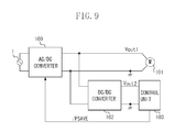
- FIG. 9 illustrates an example of a block diagram of a device that includes a typical switching power supply.
- an AC/DC converter 100 transforms an alternating-current voltage from a commercial power supply 1 to a direct-current voltage Vout 1 .
- the voltage Vout 1 is supplied to an actuator 101 such as a motor.
- the voltage Vout 1 is also supplied to a DC/DC converter 102 .
- the DC/DC converter 102 transforms the voltage Vout 1 to a direct-current voltage Vout 2 .
- the voltage Vout 2 is supplied to a control unit 103 configured to control the device.
- the power supply voltage Vout 1 for the actuator 101 is set higher than the power supply voltage Vout 2 for the control unit 103 .
- DC represents an alternating-current voltage
- DC represents a direct-current voltage.
- FIG. 10 is a circuit diagram of a switching power supply including an AC/DC converter 100 for converting an alternating-current voltage from a commercial power supply into a direct-current voltage, and a DC/DC converter 102 for converting the direct-current voltage from the AC/DC converter 100 into a different direct-current voltage.
- the AC/DC converter serves as a first converter and the DC/DC converter serves as a second converter.
- the output voltage of the AC/DC converter is a first voltage and the output voltage of the DC/DC converter is a second voltage.
- the switching power supply is discussed as a switching power supply that outputs a first voltage of 24.0 V and a second voltage of 3.30 V. Next, a basic operation of the switching power supply will be described.
- the AC/DC converter 100 serving as a first converter will be described.
- the alternating-current voltage of the commercial power supply 1 is rectified and smoothed by a bridge diode 2 and a primary smoothing capacitor 3 and output as a direct-current voltage.
- the direct-current voltage is supplied to a field-effect transistor (FET) 9 serving as a switching element via a primary winding 10 p of a transformer.
- FET field-effect transistor
- PWM pulse-width modulation
- the FET 9 thus performs PWM switching based on error information of the output voltage fed back to the photocoupler 8 p .
- PWM switching When PWM switching is performed, this introduces a pulse voltage to a secondary winding 10 s of the transformer.
- This pulse voltage is rectified and smoothed by a diode 11 and a secondary smoothing capacitor 12 and is output as a direct-current voltage Vout 1 .
- the voltage Vout 1 is supplied to an error amplifier circuit including resistors 15 , 16 , and 13 , a shunt regulator 14 , and a photocoupler 8 s .
- the FET 9 thus performs PWM switching based on the error information of the voltage Vout 1 . With this configuration, the voltage Vout 1 is made constant.
- the output voltage Vout 1 of the AC/DC converter 100 is supplied, as an input voltage to the DC/DC converter 102 , to an FET 30 serving as a switching element.
- an FET 30 serving as a switching element.
- a push-pull circuit including transistors 27 and 28 is connected via a resistor 29 .
- This push-pull circuit functions as a drive unit for driving the FET 30 .
- the push-pull circuit is used to enhance the speed of switching by enhancing the speed of charging and discharging of a gate input charge Qg of the FET 30 .
- a PWM circuit serving as a pulse signal generating unit and including resistors 25 and 24 , a transistor 26 , comparators 23 , 22 , a triangular wave generator 20 , and a constant voltage source 21 is connected.
- This PWM circuit outputs a pulse signal (hereinafter, also referred to as a PWM signal) for switching the FET 30 .
- the FET 30 performs PWM switching based on a PWM signal that is output based on error information of the output voltage fed back to the comparator 22 .
- the pulse voltage is supplied to an inductor 31 and a diode 32 .
- This pulse voltage is commutated by the inductor 31 , the diode 32 , and an electrolytic capacitor 33 and output as an output voltage Vout 2 .
- the output voltage Vout 2 is divided by resistors 34 and 35 and supplied to the comparator 22 .
- the FET 30 performs PWM switching based on the error information of the voltage Vout 2 .
- the voltage Vout 2 is made constant.
- the above-described PWM signal is a pulse width modulation signal and “PWM switching” refers to a switching operation of the FET according to a time width of the pulse width modulation signal.
- a power saving signal (hereinafter, referred to as a /PSAVE signal) is supplied from the control unit 103 to the AC/DC converter 100 .
- a /PSAVE signal is supplied from the control unit 103 to the AC/DC converter 100 .
- the output voltage of the AC/DC converter 100 is reduced.
- the operating state is switched to the power saving mode to realize reduction of power consumption while the FET 30 of the DC/DC converter 102 is kept in an on state constantly.
- an ON threshold voltage to keep the general FET constantly in an on state is often equal to or greater than 2.5 V, for example.
- a gate terminal voltage of the FET is lower than 2.5 V in the power saving mode, a case where the FET cannot certainly be turned on may occur in the switching power supply illustrated in FIG. 9 .
- the ON threshold voltage becomes lower than 2.5 V.
- an element that has a low ON threshold voltage can be used.
- an FET having a low ON threshold voltage may be expensive since a finer semiconductor process is to be used to manufacture such an FET to improve the sensitivity of its gate terminal.
- a converter includes a switching element configured to switch an input voltage, a drive unit configured to drive the switching element, a pulse signal generating unit configured to supply a pulse signal to the drive unit, and a bypass unit configured to connect the switching element and the pulse signal generating unit without involving the drive unit.
- An operation of the bypass unit maintains the switching element in an on state when the input voltage is switched to a lower voltage and switching of the input voltage is stopped.
- FIGS. 1A and 1B are circuit block diagrams of a switching power supply according to a first exemplary embodiment of the present invention.
- FIG. 2 is a diagram illustrating an operating state of the switching power supply according to the first exemplary embodiment.
- FIGS. 3A to 3C are diagrams illustrating modifications of the circuit configuration of the switching power supply according to the first exemplary embodiment.
- FIG. 4 is a diagram illustrating an operating state of the switching power supply according to the first exemplary embodiment.
- FIGS. 5A and 5B are circuit block diagrams of a switching power supply according to a second exemplary embodiment of the present invention.
- FIG. 6 is a diagram illustrating an operating state of the switching power supply according to the second exemplary embodiment.
- FIGS. 7A and 7B are circuit block diagrams of a switching power supply according to a third exemplary embodiment of the present invention.
- FIG. 8 is a diagram illustrating an operating state of the switching power supply according to the third exemplary embodiment.
- FIG. 9 is a block diagram of a switching power supply.
- FIG. 10 is a circuit block diagram of a switching power supply.
- FIG. 11 is a diagram illustrating an operating state of a switching power supply.
- FIG. 12 is a circuit block diagram of a switching power supply.
- FIGS. 9 , 10 , 11 , and 12 Prior to describing a configuration of an exemplary embodiment of the present invention, an issue in a background configuration of the present invention will be described with reference to FIGS. 9 , 10 , 11 , and 12 .
- the control unit 103 supplies a /PSAVE signal of high (H) level to set the device in a normal mode or a /PSAVE signal of low (L) level to set the device in a power saving mode.
- the /PSAVE signal is supplied to an FET 18 in the error amplifier circuit of the AC/DC converter 100 .
- the normal mode that is, when the /PSAVE signal is in H level, the FET 18 is turned on and the resistor 16 and the resistor 17 are connected in parallel.
- the output voltage Vout 1 is divided by the resistor 15 and the parallel resistors (resistor 16 //resistor 17 ) and the divided voltage is supplied to a reference terminal of the shunt regulator 14 .
- respective resistance values of the resistors 15 , 16 , and 17 are represented by “Ra”, “Rb”, and “Rc”, and a reference voltage of the shunt regulator 14 is represented by “Vref 1 ”
- Vref 1 an output voltage Vout 1 -N in the normal mode is approximately expressed by Equation (1).
- Equation (2) is a parallel resistance value of Rb and Rc and expressed by Equation (2).
- the output voltage Vout 1 -S in the power saving mode becomes lower than the output voltage Vout 1 -N in the normal mode.
- the output voltage Vout 2 of the DC/DC converter 102 can be obtained in the same manner.
- the voltage obtained by dividing the voltage Vout 2 by the resistor 34 and the resistor 35 is supplied to the comparator 22 in the error amplifier circuit and compared with the voltage of the constant voltage source 21 .
- the output voltage Vout 2 is approximately expressed by Equation (4).
- the resistance values Ra, Rb, Rc, Rd, and Re are set so that the output voltages of the AC/DC converter 100 and the DC/DC converter 102 are set as expressed by the following equations.
- the output voltage Vout 1 -S of the AC/DC converter 100 in the power saving mode is set slightly lower than the output voltage Vout 2 of the DC/DC converter 102 .
- the set value of the output voltage Vout 1 -S can be selected as appropriate within a range of operation power supply voltages of the control unit 103 .
- V out ⁇ ⁇ 1 - N ⁇ R a + ( R b // R c ) ( R b // R c ) ⁇ V ref ⁇ ⁇ 1 24.0 ⁇ [ V ] ( 5 )
- V out ⁇ ⁇ 1 - S ⁇ R a + R b R b ⁇ V ref ⁇ ⁇ 1 3.20 ⁇ [ V ] ( 6 )
- V out ⁇ ⁇ 2 ⁇ R d + R e R e ⁇ V ref ⁇ ⁇ 2 3.30 ⁇ [ V ] ( 7 )
- the control unit 103 sets the device in the normal mode by supplying a /PSAVE signal of H level.
- a PWM pulse is supplied to the gate terminal of the FET 30 and the FET 30 performs a switching operation according to the PWM pulse.
- the control unit 103 supplies a /PSAVE signal of L level to shift the mode of the device to the power saving mode. Then, the output voltage Vout 1 of the AC/DC converter 100 starts to be lowered and becomes 3.20 V after time t 2 .
- the description will focus on the operation of the DC/DC converter 102 .
- a PWM pulse is supplied to the gate terminal of the FET 30 and the FET 30 performs switching.
- the output voltage of the DC/DC converter 102 is made constant at 3.30 V.
- the output voltage of the DC/DC converter 102 cannot be kept at 3.30 V, which is a control target, so that the FET 30 is kept in an on state constantly. In other words, the FET 30 does not perform switching and stays in a conductive state in which the on state is maintained.
- the output voltage of the DC/DC converter 102 becomes approximately equal to the output voltage of the AC/DC converter 100 and becomes 3.20 V after time t 2 .
- the output voltage of the AC/DC converter 100 is made equal to or lower than the control target voltage of the DC/DC converter 102 to keep the FET 30 of the DC/DC converter 102 in an on state constantly.
- the following effect for reducing power consumption can be obtained. First, when the output voltage Vout 1 of the AC/DC converter 100 is made lower, power consumption in the actuator 101 is reduced. Further, when the switching by the FET 30 stops, switching loss is prevented.
- the configuration that is capable of reducing the output voltage of the AC/DC converter 100 and keeping the FET 30 of the DC/DC converter 102 in an on state constantly in such a power saving mode has the following issue.
- a gate-to-source voltage Vgs of the FET 30 becomes lower than the output voltage Vout 1 -S of the AC/DC converter 100 by an amount of Vce+Vbe.
- Vce is an emitter-to-collector voltage of the transistor 26 and “Vbe” is a base-to-emitter voltage of the transistor 28 .
- Vgs is approximately expressed by Equation (8). V gs ⁇ V out1-S ⁇ ( V ce +V be ) (8)
- an FET having a lower ON threshold voltage or an FET having an ON threshold voltage Vgs-on of 1.5 V can be used, for example.
- an FET having a low ON threshold voltage is expensive since such an FET is manufactured in a finer semiconductor process to improve its gate sensitivity. Thus, it is difficult to reliably turn on the FET with an inexpensive circuit configuration.
- an FET having a lower ON threshold voltage tends to have a lower drain-source withstand voltage Vdss since such an FET is made in a fine process.
- an FET 30 having a high drain-source withstand voltage Vdss is to be used.
- the voltage Vdss is not sufficient.
- an FET having the voltage Vdss of 30 V or 40 V is to be used.
- an FET having an ON threshold voltage Vgs-on of 1.5 V is not applicable since the voltage Vdss is approximately 10 V to 20 V.
- FIG. 1A illustrates a circuit configuration of a DC/DC converter according to the first exemplary embodiment.
- the present exemplary embodiment has a configuration in which a bypass resistor 40 is provided between the gate terminal of the FET 30 and a collector terminal of the transistor 26 in addition to the above-described DC/DC converter 102 in FIG. 10 .
- the bypass resistor 40 serves as a bypass unit configured to charge an input capacitance of the FET.
- the gate-to-source voltage Vgs of the FET 30 becomes smaller than the output voltage Vout 1 -S of the AC/DC converter 100 by an amount of Vce+Vbe at time t 1 .
- Vce represents an emitter-to-collector voltage of the transistor 26
- Vbe represents a base-to-emitter voltage of the transistor 28 .
- the voltage “Vgs” is approximately expressed in Equation (9). V gs ⁇ V out1-S ⁇ ( V ce +V be ) (9)
- the input capacitance of the FET 30 is to be charged via the bypass resistor 40 .
- the input capacitance of the FET 30 is represented by “Ciss” and the resistance value of the bypass resistor 40 is represented by “Rv”
- the input capacitance of the FET 30 is charged with the time constant of Ciss and Rv, and the base-to-emitter voltage Vbe of the transistor 28 becomes approximately 0.
- the gate-to-source voltage of the FET 30 is expressed by Equation (10).
- the voltage applied between the base and emitter of the transistor 28 can be made approximately 0 V, so that the gate-to-source voltage of the FET 30 can be increased.
- the voltage Vout 1 -S is 3.20 V.
- the input capacitance of the FET 30 is to be charged via the bypass resistor 40 .
- the input capacitance of the FET 30 is represented by “Ciss” and the resistance value of the bypass resistor 40 is represented by “Rv”
- the input capacitance of the FET 30 is charged with the time constant of Ciss and Rv, and the emitter-to-collector voltage Vce of the transistor 26 and the base-to-emitter voltage Vbe of the transistor 28 become approximately 0 V.
- the gate-to-source voltage of the FET 30 is expressed by Equation (12). V gs ⁇ V out1-S (12)
- the resistor 25 and the transistor 27 are apparently equivalent to the resistance represented by resistance value “Rp/hfe.”
- Rp represents a resistance value of the resistor 25
- hfe represents a current amplification rate of the transistor 27 .
- the voltage expressed by Equation (13) as the gate-to-source voltage Vgs′ of the FET 30 may remain.
- the resistance value of the resistor 29 is assumed to be sufficiently smaller than Rv and Rp/hfe.
- V gs ′ V out ⁇ ⁇ 1 - N R V + R p / h fe ⁇ R p / h fe ( 13 )
- the FET can be reliably turned on in the power saving mode.
- FIG. 5A illustrates a circuit configuration according to the second exemplary embodiment.
- This circuit configuration represents a circuit in which a diode 41 is provided as a substitute for the transistor 28 in the DC/DC converter in FIG. 1A in the first exemplary embodiment.
- an NPN transistor 27 enhances the speed to turn off the FET 30 and a PNP transistor 26 enhances the speed to turn on the FET 30 .
- the transistor 28 in FIG. 1A can be replaced with the diode 41 as illustrated in FIG. 5A according to the present exemplary embodiment.
- the gate-to-source voltage Vgs of the FET 30 becomes lower than the output voltage Vout 1 -S of the AC/DC converter 100 by an amount of Vce+Vf at time t 1 .
- Vce represents the emitter-to-collector voltage of the transistor 26 and “Vf” represents a forward voltage of the diode 41 .
- Vgs can be expressed approximately by Equation (14). V gs ⁇ V out1-S ⁇ ( V ce +V f ) (14)
- the input capacitance of the FET 30 is to be charged via the bypass resistor 40 .
- the input capacitance of the FET 30 is represented by “Ciss” and the resistance value of the bypass resistor 40 is represented by “Rv,” the input capacitance of the FET 30 is charged with the time constant of Ciss and Rv, and the forward voltage Vf of the diode 41 becomes approximately 0.
- the bypass resistor 40 is added between the gate terminal of the FET 30 and the collector terminal of the transistor 26 , the voltage applied between the anode and the cathode of the diode 41 can be made approximately 0 V and the gate-to-source voltage of the FET 30 can be increased.
- the FET can be reliably turned on during the power saving mode with an inexpensive circuit configuration including a universal element.
- FIG. 7A illustrates a circuit configuration of the present exemplary embodiment.
- This circuit configuration includes a diode 42 as a substitute for the transistor 27 in the DC/DC converter in the first exemplary embodiment illustrated in FIG. 1A .
- the NPN transistor 27 enhances the speed to turn off the FET 30 and the PNP transistor 28 enhances the speed to turn on the FET 30 .
- the transistor 27 in FIG. 1A may be replaced with the diode 42 as illustrated in FIG. 7A .
- the gate-to-source voltage Vgs of the FET 30 is lower than the output voltage Vout 1 -S of the AC/DC converter by an amount of Vce+Vbe at time t 1 .
- Vce represents an emitter-to-collector voltage of the transistor 26
- Vbe represents a base-to-emitter voltage of the transistor 28 .
- the voltage Vgs can be expressed approximately by Equation (16). V gs ⁇ V out1-S ⁇ ( V ce +V be ) (16)
- the input capacitance of the FET 30 is to be charged via the bypass resistor 40 .
- the input capacitance of the FET 30 is represented by “Ciss” and the resistance value of the bypass resistor 40 is represented by “Rv”
- the input capacitance of the FET 30 is charged with the time constant of Ciss and Rv, and the base-to-emitter voltage Vbe of the transistor 28 becomes approximately 0.
- the gate-to-source voltage Vgs of the FET 30 is expressed by Equation (17).
- the bypass resistor 40 when the bypass resistor 40 is added between the gate terminal of the FET 30 and the collector terminal of the transistor 26 , the voltage applied between the base and emitter of the transistor 28 can be made approximately 0 and the gate-to-source voltage of the FET 30 is gained.
- the switching power supply having the DC/DC converter described in the above first to third exemplary embodiments can be applied to an image forming apparatus that forms an image on a recording material, for example.
- the image forming apparatus include a copying machine, which copies an original document, and a printer, such as a laser-beam printer or an inkjet printer, which operates in response to instructions from a computer.
- the output voltage (Vpout 1 ) from the AC/DC converter in the above-described first to third exemplary embodiments is supplied to a drive motor serving as an image forming driving unit of the image forming apparatus, and the output voltage (Vout 2 ) from the DC/DC converter is supplied to a control unit including a CPU.
- the drive motor of the image forming apparatus include a drive motor for a conveyance roller that conveys recording sheets, and a motor that drives the image forming driving unit.
- Such an image forming apparatus has a power saving mode for reducing power consumption during a standby state when image formation is not performed, in addition to an operation mode for forming images.
- the switching power supply can be shifted to the power saving mode as described above by turning off the power supplied to the drive motor. In other words, the switching power supply is shifted to a state in which power is supplied only to the control unit.
Landscapes
- Engineering & Computer Science (AREA)
- Power Engineering (AREA)
- Dc-Dc Converters (AREA)
- Rectifiers (AREA)
Abstract
Description
V gs ≅V out1-S−(V ce +V be) (8)
V gs ≅V out1-S−(V ce +V be) (9)
V gs ≅V out1-S −V ce (10)
V gs ≅V out1-S−(V ce +V be) (11)
V gs ≅V out1-S (12)
V gs ≅V out1-S−(V ce +V f) (14)
V gs ≅V out1-S −V ce (15)
V gs ≅V out1-S−(V ce +V be) (16)
V gs ≅V out1-S −V ce (17)
Claims (11)
Applications Claiming Priority (2)
| Application Number | Priority Date | Filing Date | Title |
|---|---|---|---|
| JP2009070181A JP5558729B2 (en) | 2009-03-23 | 2009-03-23 | Converter, switching power supply, and image forming apparatus |
| JP2009-070181 | 2009-03-23 |
Publications (2)
| Publication Number | Publication Date |
|---|---|
| US20100239303A1 US20100239303A1 (en) | 2010-09-23 |
| US8718504B2 true US8718504B2 (en) | 2014-05-06 |
Family
ID=42737745
Family Applications (1)
| Application Number | Title | Priority Date | Filing Date |
|---|---|---|---|
| US12/727,782 Active 2031-03-30 US8718504B2 (en) | 2009-03-23 | 2010-03-19 | Converter and switching power supply for turning on switching unit according to decline of input voltage, and image forming apparatus including the switching power supply |
Country Status (4)
| Country | Link |
|---|---|
| US (1) | US8718504B2 (en) |
| JP (1) | JP5558729B2 (en) |
| KR (1) | KR101263065B1 (en) |
| CN (1) | CN101847930B (en) |
Families Citing this family (12)
| Publication number | Priority date | Publication date | Assignee | Title |
|---|---|---|---|---|
| US8816654B2 (en) * | 2010-09-27 | 2014-08-26 | Cooper Technologies Company | Universal-voltage discrete input circuit |
| JP5737963B2 (en) * | 2011-01-21 | 2015-06-17 | キヤノン株式会社 | Switching power supply and image forming apparatus having switching power supply |
| JP5582055B2 (en) * | 2011-02-14 | 2014-09-03 | ブラザー工業株式会社 | Image forming apparatus |
| US8866404B2 (en) * | 2011-06-08 | 2014-10-21 | Shenzhen China Star Optoelectronics Technology Co., Ltd. | Backlight module and display apparatus |
| US8659279B2 (en) * | 2011-07-14 | 2014-02-25 | Cooper Technologies Company | Automatic power converter bypass |
| JP5889570B2 (en) * | 2011-08-18 | 2016-03-22 | 立川ブラインド工業株式会社 | DC motor control device, electric solar shading device, and DC motor control method |
| JP5990979B2 (en) * | 2012-03-30 | 2016-09-14 | ブラザー工業株式会社 | Image forming apparatus |
| JP6016429B2 (en) | 2012-04-18 | 2016-10-26 | キヤノン株式会社 | Power supply control device, image forming apparatus |
| CN105518993B (en) * | 2013-09-06 | 2019-04-16 | 三菱电机株式会社 | Buffer circuit |
| CN106143170B (en) * | 2015-03-31 | 2020-11-17 | 通用电气公司 | Energy storage system with range extender and energy management control method |
| CN109450274A (en) * | 2018-12-28 | 2019-03-08 | 联想(北京)有限公司 | A kind of control method, device and electronic equipment |
| CN114902157B (en) * | 2020-03-30 | 2024-06-11 | 松下新能源株式会社 | Electronic circuit unit and battery pack |
Citations (9)
| Publication number | Priority date | Publication date | Assignee | Title |
|---|---|---|---|---|
| JPS60257766A (en) | 1984-05-31 | 1985-12-19 | Panafacom Ltd | Dc-dc power converter |
| JPH07146719A (en) | 1993-11-22 | 1995-06-06 | Matsushita Electric Ind Co Ltd | Power supply for portable GPS receiver |
| JP2001178117A (en) | 1999-12-17 | 2001-06-29 | Pfu Ltd | Power circuit |
| JP2003266878A (en) | 2002-03-19 | 2003-09-25 | Ricoh Co Ltd | Image forming device |
| US20030205990A1 (en) * | 2002-05-01 | 2003-11-06 | Wittenbreder, Ernest H. | Circuits and circuit elements for high efficiency power conversion |
| US20050068794A1 (en) * | 2003-09-26 | 2005-03-31 | Hsiang-Chung Weng | Active clamping circuit and power supply system using the same |
| JP2006067703A (en) | 2004-08-26 | 2006-03-09 | Sharp Corp | Switching power supply device |
| KR100666829B1 (en) | 2005-11-29 | 2007-01-10 | 단암전자통신주식회사 | Switching Device for Multiple Output Power Supply |
| JP2008067494A (en) | 2006-09-07 | 2008-03-21 | Canon Inc | Power supply device and image forming apparatus |
Family Cites Families (6)
| Publication number | Priority date | Publication date | Assignee | Title |
|---|---|---|---|---|
| JPH07162279A (en) * | 1993-12-09 | 1995-06-23 | Hitachi Ltd | Transistor output circuit, sequencer, switching power supply, inverter |
| JP3036457B2 (en) * | 1997-02-27 | 2000-04-24 | 日本電気株式会社 | Switching power supply |
| JP2001045742A (en) * | 1999-07-29 | 2001-02-16 | Nissan Motor Co Ltd | Power MOS drive circuit |
| JP2003143831A (en) * | 2001-11-06 | 2003-05-16 | Fuji Electric Co Ltd | Gate drive circuit |
| US20050068784A1 (en) * | 2003-09-30 | 2005-03-31 | Lee Seung Sin | Lamp device for eliminating blind spot in automotive vehicle |
| JP2007282411A (en) * | 2006-04-10 | 2007-10-25 | Rohm Co Ltd | Step-up dc/dc converter and electronic apparatus having the same |
-
2009
- 2009-03-23 JP JP2009070181A patent/JP5558729B2/en active Active
-
2010
- 2010-03-19 US US12/727,782 patent/US8718504B2/en active Active
- 2010-03-23 CN CN201010150768.9A patent/CN101847930B/en active Active
- 2010-03-23 KR KR1020100025804A patent/KR101263065B1/en active Active
Patent Citations (9)
| Publication number | Priority date | Publication date | Assignee | Title |
|---|---|---|---|---|
| JPS60257766A (en) | 1984-05-31 | 1985-12-19 | Panafacom Ltd | Dc-dc power converter |
| JPH07146719A (en) | 1993-11-22 | 1995-06-06 | Matsushita Electric Ind Co Ltd | Power supply for portable GPS receiver |
| JP2001178117A (en) | 1999-12-17 | 2001-06-29 | Pfu Ltd | Power circuit |
| JP2003266878A (en) | 2002-03-19 | 2003-09-25 | Ricoh Co Ltd | Image forming device |
| US20030205990A1 (en) * | 2002-05-01 | 2003-11-06 | Wittenbreder, Ernest H. | Circuits and circuit elements for high efficiency power conversion |
| US20050068794A1 (en) * | 2003-09-26 | 2005-03-31 | Hsiang-Chung Weng | Active clamping circuit and power supply system using the same |
| JP2006067703A (en) | 2004-08-26 | 2006-03-09 | Sharp Corp | Switching power supply device |
| KR100666829B1 (en) | 2005-11-29 | 2007-01-10 | 단암전자통신주식회사 | Switching Device for Multiple Output Power Supply |
| JP2008067494A (en) | 2006-09-07 | 2008-03-21 | Canon Inc | Power supply device and image forming apparatus |
Non-Patent Citations (3)
| Title |
|---|
| Kim, Hee-Joon, "Basic Design of Switched-Mode Power Supply," Book Media Group Sung An Dang (www.cyber.co.kr/www.sungandang.com), pp. 1-34. |
| Machine English Translation of JP2003-266878 published on Sep. 25, 2003. * |
| U.S. Appl. No. 12/721,963, filed Mar. 11, 2010, Yasuhiro Nakata. |
Also Published As
| Publication number | Publication date |
|---|---|
| JP5558729B2 (en) | 2014-07-23 |
| JP2010226845A (en) | 2010-10-07 |
| US20100239303A1 (en) | 2010-09-23 |
| CN101847930B (en) | 2015-05-06 |
| KR101263065B1 (en) | 2013-05-09 |
| CN101847930A (en) | 2010-09-29 |
| KR20100106248A (en) | 2010-10-01 |
Similar Documents
| Publication | Publication Date | Title |
|---|---|---|
| US8718504B2 (en) | Converter and switching power supply for turning on switching unit according to decline of input voltage, and image forming apparatus including the switching power supply | |
| JP5735792B2 (en) | Comparator, switching regulator control circuit using it, switching regulator, electronic equipment | |
| US9621061B2 (en) | Power supply apparatus and image forming apparatus | |
| US9612604B2 (en) | DC-DC converter and television receiver therewith | |
| US20080169793A1 (en) | Semiconductor apparatus | |
| JP4033082B2 (en) | DC-DC converter | |
| JP2008079448A (en) | Boost power supply | |
| JP2005287248A (en) | Switching power supply | |
| JP4682647B2 (en) | Switching power supply | |
| JP5988566B2 (en) | Power supply and image forming apparatus | |
| CN116111848A (en) | Integrated Circuits and Power Circuits | |
| JP7175699B2 (en) | Power supply and image forming apparatus | |
| JP2011010396A (en) | Switching element driving circuit, and converter | |
| US20130272742A1 (en) | Dc/dc converter and image forming apparatus including the same | |
| CN110326200B (en) | switch control device | |
| US9154043B2 (en) | Power source device and image forming apparatus | |
| US20080094264A1 (en) | Digital-to-Analog Converting Circuit for Power Soft-Switching | |
| US10175632B2 (en) | Power supply and image forming apparatus | |
| JP2003061352A (en) | Dc-dc converter | |
| JP3757293B2 (en) | DC-DC converter | |
| JP7603484B2 (en) | Semiconductor drive circuit and power conversion device | |
| JP2002136108A (en) | Voltage-boosting circuit | |
| JP2007159305A (en) | Power supply | |
| US11038429B2 (en) | Insulation-type switching power supply | |
| JP3419343B2 (en) | DC-DC converter |
Legal Events
| Date | Code | Title | Description |
|---|---|---|---|
| AS | Assignment |
Owner name: CANON KABUSHIKI KAISHA, JAPAN Free format text: ASSIGNMENT OF ASSIGNORS INTEREST;ASSIGNOR:MATSUMOTO, SHINICHIRO;REEL/FRAME:024490/0333 Effective date: 20100226 |
|
| STCF | Information on status: patent grant |
Free format text: PATENTED CASE |
|
| MAFP | Maintenance fee payment |
Free format text: PAYMENT OF MAINTENANCE FEE, 4TH YEAR, LARGE ENTITY (ORIGINAL EVENT CODE: M1551) Year of fee payment: 4 |
|
| MAFP | Maintenance fee payment |
Free format text: PAYMENT OF MAINTENANCE FEE, 8TH YEAR, LARGE ENTITY (ORIGINAL EVENT CODE: M1552); ENTITY STATUS OF PATENT OWNER: LARGE ENTITY Year of fee payment: 8 |