US8704995B2 - Liquid crystal display device, panel and panel manufacture method thereof - Google Patents
Liquid crystal display device, panel and panel manufacture method thereof Download PDFInfo
- Publication number
- US8704995B2 US8704995B2 US13/574,601 US201213574601A US8704995B2 US 8704995 B2 US8704995 B2 US 8704995B2 US 201213574601 A US201213574601 A US 201213574601A US 8704995 B2 US8704995 B2 US 8704995B2
- Authority
- US
- United States
- Prior art keywords
- substrate
- seal
- adjacent
- conductive particles
- common electrodes
- Prior art date
- Legal status (The legal status is an assumption and is not a legal conclusion. Google has not performed a legal analysis and makes no representation as to the accuracy of the status listed.)
- Active, expires
Links
Images


Classifications
-
- G—PHYSICS
- G02—OPTICS
- G02F—OPTICAL DEVICES OR ARRANGEMENTS FOR THE CONTROL OF LIGHT BY MODIFICATION OF THE OPTICAL PROPERTIES OF THE MEDIA OF THE ELEMENTS INVOLVED THEREIN; NON-LINEAR OPTICS; FREQUENCY-CHANGING OF LIGHT; OPTICAL LOGIC ELEMENTS; OPTICAL ANALOGUE/DIGITAL CONVERTERS
- G02F1/00—Devices or arrangements for the control of the intensity, colour, phase, polarisation or direction of light arriving from an independent light source, e.g. switching, gating or modulating; Non-linear optics
- G02F1/01—Devices or arrangements for the control of the intensity, colour, phase, polarisation or direction of light arriving from an independent light source, e.g. switching, gating or modulating; Non-linear optics for the control of the intensity, phase, polarisation or colour
- G02F1/13—Devices or arrangements for the control of the intensity, colour, phase, polarisation or direction of light arriving from an independent light source, e.g. switching, gating or modulating; Non-linear optics for the control of the intensity, phase, polarisation or colour based on liquid crystals, e.g. single liquid crystal display cells
- G02F1/133—Constructional arrangements; Operation of liquid crystal cells; Circuit arrangements
- G02F1/1333—Constructional arrangements; Manufacturing methods
- G02F1/1339—Gaskets; Spacers; Sealing of cells
-
- G—PHYSICS
- G02—OPTICS
- G02F—OPTICAL DEVICES OR ARRANGEMENTS FOR THE CONTROL OF LIGHT BY MODIFICATION OF THE OPTICAL PROPERTIES OF THE MEDIA OF THE ELEMENTS INVOLVED THEREIN; NON-LINEAR OPTICS; FREQUENCY-CHANGING OF LIGHT; OPTICAL LOGIC ELEMENTS; OPTICAL ANALOGUE/DIGITAL CONVERTERS
- G02F1/00—Devices or arrangements for the control of the intensity, colour, phase, polarisation or direction of light arriving from an independent light source, e.g. switching, gating or modulating; Non-linear optics
- G02F1/01—Devices or arrangements for the control of the intensity, colour, phase, polarisation or direction of light arriving from an independent light source, e.g. switching, gating or modulating; Non-linear optics for the control of the intensity, phase, polarisation or colour
- G02F1/13—Devices or arrangements for the control of the intensity, colour, phase, polarisation or direction of light arriving from an independent light source, e.g. switching, gating or modulating; Non-linear optics for the control of the intensity, phase, polarisation or colour based on liquid crystals, e.g. single liquid crystal display cells
- G02F1/133—Constructional arrangements; Operation of liquid crystal cells; Circuit arrangements
- G02F1/1333—Constructional arrangements; Manufacturing methods
- G02F1/133351—Manufacturing of individual cells out of a plurality of cells, e.g. by dicing
-
- G—PHYSICS
- G02—OPTICS
- G02F—OPTICAL DEVICES OR ARRANGEMENTS FOR THE CONTROL OF LIGHT BY MODIFICATION OF THE OPTICAL PROPERTIES OF THE MEDIA OF THE ELEMENTS INVOLVED THEREIN; NON-LINEAR OPTICS; FREQUENCY-CHANGING OF LIGHT; OPTICAL LOGIC ELEMENTS; OPTICAL ANALOGUE/DIGITAL CONVERTERS
- G02F1/00—Devices or arrangements for the control of the intensity, colour, phase, polarisation or direction of light arriving from an independent light source, e.g. switching, gating or modulating; Non-linear optics
- G02F1/01—Devices or arrangements for the control of the intensity, colour, phase, polarisation or direction of light arriving from an independent light source, e.g. switching, gating or modulating; Non-linear optics for the control of the intensity, phase, polarisation or colour
- G02F1/13—Devices or arrangements for the control of the intensity, colour, phase, polarisation or direction of light arriving from an independent light source, e.g. switching, gating or modulating; Non-linear optics for the control of the intensity, phase, polarisation or colour based on liquid crystals, e.g. single liquid crystal display cells
- G02F1/133—Constructional arrangements; Operation of liquid crystal cells; Circuit arrangements
- G02F1/1333—Constructional arrangements; Manufacturing methods
- G02F1/1339—Gaskets; Spacers; Sealing of cells
- G02F1/13398—Spacer materials; Spacer properties
-
- G—PHYSICS
- G02—OPTICS
- G02F—OPTICAL DEVICES OR ARRANGEMENTS FOR THE CONTROL OF LIGHT BY MODIFICATION OF THE OPTICAL PROPERTIES OF THE MEDIA OF THE ELEMENTS INVOLVED THEREIN; NON-LINEAR OPTICS; FREQUENCY-CHANGING OF LIGHT; OPTICAL LOGIC ELEMENTS; OPTICAL ANALOGUE/DIGITAL CONVERTERS
- G02F2201/00—Constructional arrangements not provided for in groups G02F1/00 - G02F7/00
- G02F2201/12—Constructional arrangements not provided for in groups G02F1/00 - G02F7/00 electrode
- G02F2201/121—Constructional arrangements not provided for in groups G02F1/00 - G02F7/00 electrode common or background
-
- G—PHYSICS
- G02—OPTICS
- G02F—OPTICAL DEVICES OR ARRANGEMENTS FOR THE CONTROL OF LIGHT BY MODIFICATION OF THE OPTICAL PROPERTIES OF THE MEDIA OF THE ELEMENTS INVOLVED THEREIN; NON-LINEAR OPTICS; FREQUENCY-CHANGING OF LIGHT; OPTICAL LOGIC ELEMENTS; OPTICAL ANALOGUE/DIGITAL CONVERTERS
- G02F2202/00—Materials and properties
- G02F2202/16—Materials and properties conductive
Definitions
- the present invention relates to the field of liquid crystal displaying techniques, and in particular to a liquid crystal display device, panel and panel manufacture method thereof.
- FIG. 1 shows a schematic view of a coating structure of seal 20 of substrate 10 in known technique. Because coating technique determines that seal 20 must be designed as independent and closed pattern, it is a difficult task to apply transfer pad or Au in sealant on Vcom while other areas using general seal coating.
- the technical issue to be addressed by the present invention is to provide a liquid crystal display device, panel and panel manufacture method, to avoid complex process of transfer pad as well as solve the problem of applying transfer pad or Au in sealant on Vcom while other areas using general seal coating.
- the present invention provides a panel manufacture method, which comprises: completing thin film transistor array and common electrode (Vcom) on glass substrate, forming adjacent substrate pair, the adjacent substrate pair comprising a first substrate and a second substrate connected by adjacent lines, Vcom on the first substrate and the second substrate being symmetrically distributed with respect to adjacent line; coating a first seal on peripheral area of adjacent substrate pair, coating a second seal along the adjacent sides of the first substrate and the second substrate, the second seal and the first seal being partially overlapping, at least one of the first seal and the second seal comprising conductive particles; boxing the adjacent substrate pair and filter substrate pair so that conductive particles conducting common electrodes of adjacent substrate pair and filter substrate pair; cutting adjacent substrate pair and filter substrate pair along adjacent lines of first substrate and second substrate to form panel.
- Vcom thin film transistor array and common electrode
- first substrate and second substrate when the common electrode are disposed on adjacent sides of first substrate and second substrate, only second seal is doped with conductive particles and second seal at least partially covers common electrodes.
- first seal when the common electrodes are disposed on peripheral areas surrounding adjacent substrate pair, only the first seal is doped with conductive particles and first seal at least partially covers common electrodes.
- the conductive particle is gold particle (Au).
- number of conductive particles is plural and diameters of conductive particles are different.
- the width of the first seal is different width of the second seal.
- the present invention provides a panel manufactured by aforementioned panel manufacture method, which comprises: a thin film transistor substrate, being one of first substrate or second substrate; a filter substrate, being one of filter substrate pair; first seal part, a part of first seal, coating on borders of first, second and third sides of thin film transistor substrate; second seal part, a part of second seal, coating on border of fourth side of thin film transistor substrate, first seal part and second seal part being partially crossing and overlapping.
- border of the fourth side of thin film transistor substrate is disposed with common electrodes, only second seal part is doped with conductive particles and second seal part at least partially covers the common electrodes.
- borders of the first, second and third sides of thin film transistor substrate are disposed with common electrodes, only first seal part is doped with conductive particles and first seal part at least partially covers the common electrodes.
- the conductive particle is gold particle (Au).
- number of conductive particles is plural and diameters of conductive particles are different.
- the width of the first seal is different width of the second seal.
- the present invention provides a liquid crystal display device, which comprises: a thin film transistor substrate, being one of first substrate or second substrate; a filter substrate, being one of filter substrate pair; first seal part, a part of first seal, coating on borders of first, second and third sides of thin film transistor substrate; second seal part, a part of second seal, coating on border of fourth side of thin film transistor substrate, first seal part and second seal part being partially crossing and overlapping.
- border of the fourth side of thin film transistor substrate is disposed with common electrodes, only second seal part is doped with conductive particles and second seal part at least partially covers the common electrodes.
- borders of the first, second and third sides of thin film transistor substrate are disposed with common electrodes, only first seal part is doped with conductive particles and first seal part at least partially covers the common electrodes.
- the conductive particle is gold particle (Au).
- number of conductive particles is plural and diameters of conductive particles are different.
- the width of the first seal is different width of the second seal.
- the efficacy of the present invention is that to be distinguished from the state of the art.
- the liquid crystal display device, panel and panel manufacture method thereof coat the common electrode area of adjacent substrate pair with a seal doped with conductive particles, and remaining area with general seal. Through adjacent substrate pair to realize sealing coating of the seal, the panel forms different seals on different sides after cutting.
- the seal doped with conductive particle of the panel of the present invention can conduct common electrodes of the upper and lower substrates, and remaining area other than common electrode is coated with a general seal without conductive particles.
- FIG. 1 is a schematic view showing the structure of a known substrate seal coating
- FIG. 2 is a flowchart of the panel manufacture method according to the present invention.
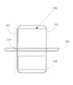
- FIG. 3 is a schematic view showing the structure of a seal coating of adjacent substrate pair prior to forming the panel according to the present invention
- FIG. 4 is a schematic view showing the structure of a first embodiment of the panel according to the present invention.
- FIG. 5A is a partial cross-sectional view showing A area of the panel of FIG. 4 ;
- FIG. 5B is a partial cross-sectional view showing B area of the panel of FIG. 4 ;
- FIG. 6A and FIG. 6B are schematic views showing the structure of a second embodiment of the panel according to the present invention.
- the panel manufacture method of the present invention comprises the steps of:
- Step S 101 completing thin film transistor array and common electrode (Vcom) on glass substrate, forming adjacent substrate pair, the adjacent substrate pair comprising a first substrate and a second substrate connected by adjacent lines, Vcom on the first substrate and the second substrate being symmetrically distributed with respect to adjacent line.
- Vcom thin film transistor array and common electrode
- adjacent substrate pair 300 is similar to the known technique. The difference is in forming adjacent substrate pair 300 on glass substrate.
- Adjacent substrate pair 300 comprises first substrate 303 and second substrate 304 , connected adjacently by adjacent line 305 .
- adjacent substrate pair 300 can be used as a unit for coating closed seal. The following will describe that, after coating seal, adjacent substrate pair 300 needs to be cut into two independent substrates.
- common electrodes 401 on first substrate 303 and second substrate 304 need to be symmetrically distributed with respect to adjacent line 305 .
- the seal is likely to symmetrically covers common electrodes 401 on first substrate 303 and second substrate 304 .
- common electrodes 401 can be disposed on adjacent sides of first substrate 303 and second substrate 304 .
- the adjacent side refers to a side on first substrate 303 and second substrate 304 respectively close to adjacent line 305 .
- Common electrodes 401 can be disposed on peripheral area surrounding adjacent substrate pair 300 . The only requirement is to have common electrodes 401 on first substrate 303 and second substrate 304 symmetrically distributed with respect to adjacent line 305 .
- the instant embodiment uses an adjacent substrate pair 300 as exemplar for description but is not restricted to the exemplar.
- a plurality of adjacent substrate pairs 300 can be formed on glass substrate in an array form for subsequent process.
- Step S 102 coating a first seal on peripheral area of adjacent substrate pair, coating a second seal along the adjacent sides of the first substrate and the second substrate, the second seal and the first seal being partially overlapping, at least one of the first seal and the second seal comprising conductive particles.
- first seal 301 and second seal 302 are used to coat symmetrically disposed first substrate 303 and second substrate 304 so that first seal 301 and second seal 302 are both closed seal, and are symmetrically with respect to adjacent line 305 .
- second seal 302 can be doped with conductive particles 403 and second seal 302 is at least partially covering common electrodes 401 of adjacent substrate pair 300 . Because adjacent substrate pair 300 corresponding to first seal 301 is not disposed with common electrodes 401 on the peripheral, first seal 301 is not doped with conductive particles.
- the instant embodiment uses two seals, coats area disposed with common electrodes 401 with second seal 302 doped with conductive particles and coats area not disposed with common electrodes 401 with first seal 301 not doped with conductive particles so that adjacent substrate pair 300 realizes closed coating of the seal.
- peripheral area of panel forms different types of seals to conduct common electrodes of upper and lower substrates.
- first seal 301 when common electrodes 401 are disposed in peripheral area surrounding adjacent substrate 300 , only first seal 301 is doped with conductive particles and first seal 301 at least partially covers common electrodes 401 .
- width of seals can be changed so that first seal 301 and second seal 302 have different widths to reduce cost and improve coating efficiency.
- first seal 301 and second seal 302 does not affect the effect of coating process, and the order is determined by the manufacture process. After coating, first seal 301 and second seal 302 are partially overlapping.
- Step S 103 boxing the adjacent substrate pair and filter substrate pair so that conductive particles conducting common electrodes of adjacent substrate pair and filter substrate pair.
- adjacent substrate pair 300 and filter substrate pair are connected through first seal 301 and second seal 302 coating on adjacent substrate 300 .
- Upper surface of conductive particles 403 is in contact with common electrodes 402 on filter substrate pair, and lower surface of conductive particles 403 is in contact with common electrodes 401 on adjacent substrate pair 300 .
- Common electrodes 401 on adjacent substrate pair 300 are conductive to common electrodes 402 on filter substrate pair through conductive particles 403 .
- seal doped with conductive particles 403 is used for area disposed with common electrodes, and remaining area not disposed with common electrodes uses seal not doped with conductive particles. Because seal is independent and closed, when seal is doped with conductive particles 403 , entire seal will be doped with conductive particles 403 . To dope seal with conductive particles 403 selectively can save manufacture cost.
- Step S 104 cutting adjacent substrate pair and filter substrate pair along adjacent lines of first substrate and second substrate to form panel.
- adjacent line 305 serves as border between first substrate 303 and second substrate 304 . After cutting along adjacent line 305 between first substrate 303 and second substrate 304 , adjacent substrate pair 300 and filter substrate pair can be cut into desired size.
- adjacent substrate pair 300 and filter substrate pair are assembled into a panel shown in FIG. 4 .
- FIG. 4 is a schematic view showing the structure of a first embodiment of the panel according to the present invention.
- FIG. 5A is a partial cross-sectional view showing A area of the panel of FIG. 4
- FIG. 5B is a partial cross-sectional view showing B area of the panel of FIG. 4 .
- the panel comprises thin film transistor substrate 500 , filter substrate, first seal part 501 and second seal part 502 .
- thin film transistor substrate 500 is one of first substrate 303 or second substrate 304 .
- Thin film transistor substrate 500 further comprises first side 503 , second side 504 , third side 505 and fourth side 506 .
- Fourth side 506 of thin film transistor substrate 500 is disposed with common electrodes 401 on the border. Only second seal part 502 is doped with conductive particles 403 , and second seal part 502 at least partially covers common electrodes 401 .
- Filter substrate is one of filter substrate pair. Filter substrate is disposed oppositely to thin film transistor substrate 500 .
- First seal part 501 is a part of first seal 301 , and is coated on borders of first side 503 , second side 504 and third side 505 of thin film transistor substrate 500 .
- Second seal part 502 is a part of second seal 302 , and is coated on border of fourth side 506 of thin film transistor substrate 500 .
- First seal part 501 and second seal part 502 are partially crossing and overlapping.
- fourth side 506 of thin film transistor substrate 500 is disposed with common electrodes 401 .
- Second seal part 502 doped with conductive particles 403 is used to coat fourth side 506 .
- First seal part 501 not doped with conductive particles 403 is used to coat first side 503 , second side 504 and third side 505 of thin film transistor substrate 500 .
- Signal conduction is accomplished through lower surface of conductive particles 403 contacting common electrodes 401 of thin film transistor substrate 500 and upper surface of conductive particles 403 contacting common electrodes 402 of filter substrate.
- common electrode area of panel are coated with second seal part 502 doped with conductive particles 403 , and remaining area is coated with general seal not doped with conductive particles.
- This approach realizes two different types of seals on a same substrate and each of seals is closed. This approach also avoids the complex process of transfer pad and solves the problem of performing Au in sealant on common electrode area of a substrate while remaining area on the substrate using general seal.
- FIG. 6A and FIG. 6B are schematic views showing the structure of a second embodiment of the present invention.
- FIG. 6A and FIG. 6B show partial cross-sectional views of seal area doped with conductive particles on the panel respectively, including upper substrate 601 and lower substrate 602 .
- Diameter of conductive particle 603 in FIG. 6A is larger than diameters of conductive particles 604 , 605 of FIG. 6B .
- conductive particles 603 , 604 , 605 are gold particles (Au).
- diameter of conductive particle 603 is larger than diameters of conductive particles 604 , 605 .
- the sizes of conductive particles do not affect conductivity of conductive particles, as long as able to realize upper surface of conductive particles contacting common electrodes on upper substrate 601 and lower surface of conductive particles contacting common electrodes on lower substrate 602 .
- Conductive particles depends on the range of seal to be coated and conductive range to achieve conduction.
- Conductive particles can also be silver particles (Ag).
- the present invention further provides an embodiment of a liquid crystal display device, which comprises the aforementioned panel.
- the liquid crystal display device, panel and panel manufacture method of the present invention coat the common electrode area of adjacent substrate pair with a seal doped with conductive particles, and remaining area with general seal.
- the panel forms different seals on different sides after cutting.
- the seal doped with conductive particle of the panel of the present invention can conduct common electrodes of the upper and lower substrates, and remaining area other than common electrode is coated with a general seal without conductive particles.
Landscapes
- Physics & Mathematics (AREA)
- Nonlinear Science (AREA)
- Mathematical Physics (AREA)
- Chemical & Material Sciences (AREA)
- Crystallography & Structural Chemistry (AREA)
- General Physics & Mathematics (AREA)
- Optics & Photonics (AREA)
- Liquid Crystal (AREA)
- Devices For Indicating Variable Information By Combining Individual Elements (AREA)
Abstract
Description
Claims (18)
Applications Claiming Priority (3)
| Application Number | Priority Date | Filing Date | Title |
|---|---|---|---|
| CN201210174245.7 | 2012-05-30 | ||
| CN201210174245.7A CN102681238B (en) | 2012-05-30 | 2012-05-30 | Liquid crystal display device, panel and manufacturing method of panel |
| PCT/CN2012/076759 WO2013177825A1 (en) | 2012-05-30 | 2012-06-12 | Liquid crystal display device, panel and panel manufacturing method |
Publications (2)
| Publication Number | Publication Date |
|---|---|
| US20130321731A1 US20130321731A1 (en) | 2013-12-05 |
| US8704995B2 true US8704995B2 (en) | 2014-04-22 |
Family
ID=46813389
Family Applications (1)
| Application Number | Title | Priority Date | Filing Date |
|---|---|---|---|
| US13/574,601 Active 2032-10-08 US8704995B2 (en) | 2012-05-30 | 2012-06-12 | Liquid crystal display device, panel and panel manufacture method thereof |
Country Status (3)
| Country | Link |
|---|---|
| US (1) | US8704995B2 (en) |
| CN (1) | CN102681238B (en) |
| WO (1) | WO2013177825A1 (en) |
Families Citing this family (4)
| Publication number | Priority date | Publication date | Assignee | Title |
|---|---|---|---|---|
| CN105629593B (en) * | 2016-03-30 | 2019-08-02 | 京东方科技集团股份有限公司 | a panel |
| CN106773194B (en) * | 2016-12-30 | 2019-06-11 | 深圳市华星光电技术有限公司 | A kind of circuit substrate and display equipment |
| CN109581755A (en) * | 2018-12-18 | 2019-04-05 | 深圳市华星光电半导体显示技术有限公司 | Display panel manufacturing method and display panel |
| CN113848667B (en) * | 2021-07-29 | 2022-09-27 | 惠科股份有限公司 | Array substrate, display panel and display device |
Family Cites Families (8)
| Publication number | Priority date | Publication date | Assignee | Title |
|---|---|---|---|---|
| JP2002296574A (en) * | 2001-03-30 | 2002-10-09 | Optrex Corp | Manufacturing method for liquid crystal display panel |
| KR20050055358A (en) * | 2003-12-08 | 2005-06-13 | 엘지.필립스 엘시디 주식회사 | A large display and the fabrication method thereof |
| JP4529932B2 (en) * | 2006-03-30 | 2010-08-25 | カシオ計算機株式会社 | Liquid crystal cell assembly |
| JP4961271B2 (en) * | 2007-06-12 | 2012-06-27 | シャープ株式会社 | Liquid crystal display panel manufacturing method and liquid crystal display panel |
| CN101676776B (en) * | 2008-09-16 | 2012-02-29 | 北京京东方光电科技有限公司 | Panel and manufacturing method thereof |
| JP2010170043A (en) * | 2009-01-26 | 2010-08-05 | Toshiba Mobile Display Co Ltd | Method for manufacturing liquid crystal display element and liquid crystal display element |
| CN101989014A (en) * | 2009-08-05 | 2011-03-23 | 奇美电子股份有限公司 | Display panel, assembling method thereof and liquid crystal display |
| KR101107174B1 (en) * | 2010-03-23 | 2012-01-25 | 삼성모바일디스플레이주식회사 | Display panel and manufacturing method thereof |
-
2012
- 2012-05-30 CN CN201210174245.7A patent/CN102681238B/en not_active Expired - Fee Related
- 2012-06-12 WO PCT/CN2012/076759 patent/WO2013177825A1/en not_active Ceased
- 2012-06-12 US US13/574,601 patent/US8704995B2/en active Active
Also Published As
| Publication number | Publication date |
|---|---|
| WO2013177825A1 (en) | 2013-12-05 |
| CN102681238B (en) | 2015-04-15 |
| CN102681238A (en) | 2012-09-19 |
| US20130321731A1 (en) | 2013-12-05 |
Similar Documents
| Publication | Publication Date | Title |
|---|---|---|
| CN103048824B (en) | Liquid crystal display device and method for manufacturing the same | |
| US9651837B2 (en) | Liquid crystal display panel structure | |
| US7852451B2 (en) | Manufacturing method of liquid display device having touch screen function | |
| CN102354069B (en) | LCD panel | |
| US20220308376A1 (en) | Array substrate, manufacturing method thereof, and display panel | |
| JP2007322627A5 (en) | ||
| US9431432B2 (en) | Array substrate, method for manufacturing the same, display device | |
| US10353249B2 (en) | Thin film transistor substrate and liquid crystal display panel | |
| CN103698948B (en) | A kind of liquid crystal panel and liquid crystal display | |
| US8704995B2 (en) | Liquid crystal display device, panel and panel manufacture method thereof | |
| CN102591060A (en) | Liquid crystal display (LCD) panel and manufacture method thereof, and LCD device | |
| CN104020604A (en) | Two-sided transparent display device | |
| CN103018986B (en) | Array baseplate and preparation and driving methods thereof, and liquid crystal display panel | |
| CN107346082A (en) | Array base palte and liquid crystal display panel | |
| CN106200153A (en) | A kind of liquid crystal indicator | |
| CN103744205B (en) | Color membrane substrates and preparation method thereof, display floater and liquid crystal indicator | |
| WO2020062596A1 (en) | Display panel and display apparatus | |
| CN203480178U (en) | Array substrate and display device | |
| CN104460071A (en) | Thin film transistor array substrate and liquid crystal display panel | |
| CN103969859B (en) | A kind of substrate for display and display device | |
| CN103646612B (en) | Electrode structure, array substrate and display device | |
| KR20130039289A (en) | Liquid crystal display device and method for manufacturing the same | |
| CN103698946A (en) | TN (twisted nematic) type liquid crystal display panel, TN type liquid crystal display panel preparation method and liquid crystal display device | |
| CN105487283A (en) | LCD and LCD panel thereof | |
| US20160005369A1 (en) | Display panel and manufacturing method thereof, display device |
Legal Events
| Date | Code | Title | Description |
|---|---|---|---|
| AS | Assignment |
Owner name: SHENZHEN CHINA STAR OPTOELECTRONICS TECHNOLOGY CO. Free format text: ASSIGNMENT OF ASSIGNORS INTEREST;ASSIGNOR:LO, SHIH-HSUN;REEL/FRAME:028605/0254 Effective date: 20120615 |
|
| FEPP | Fee payment procedure |
Free format text: PAYOR NUMBER ASSIGNED (ORIGINAL EVENT CODE: ASPN); ENTITY STATUS OF PATENT OWNER: LARGE ENTITY |
|
| STCF | Information on status: patent grant |
Free format text: PATENTED CASE |
|
| MAFP | Maintenance fee payment |
Free format text: PAYMENT OF MAINTENANCE FEE, 4TH YEAR, LARGE ENTITY (ORIGINAL EVENT CODE: M1551) Year of fee payment: 4 |
|
| MAFP | Maintenance fee payment |
Free format text: PAYMENT OF MAINTENANCE FEE, 8TH YEAR, LARGE ENTITY (ORIGINAL EVENT CODE: M1552); ENTITY STATUS OF PATENT OWNER: LARGE ENTITY Year of fee payment: 8 |
|
| FEPP | Fee payment procedure |
Free format text: MAINTENANCE FEE REMINDER MAILED (ORIGINAL EVENT CODE: REM.); ENTITY STATUS OF PATENT OWNER: LARGE ENTITY |