US8669537B2 - Charged particle beam writing apparatus and method - Google Patents
Charged particle beam writing apparatus and method Download PDFInfo
- Publication number
- US8669537B2 US8669537B2 US12/560,802 US56080209A US8669537B2 US 8669537 B2 US8669537 B2 US 8669537B2 US 56080209 A US56080209 A US 56080209A US 8669537 B2 US8669537 B2 US 8669537B2
- Authority
- US
- United States
- Prior art keywords
- shot
- write data
- data
- graphics
- charged particle
- Prior art date
- Legal status (The legal status is an assumption and is not a legal conclusion. Google has not performed a legal analysis and makes no representation as to the accuracy of the status listed.)
- Active, expires
Links
Images


Classifications
-
- H—ELECTRICITY
- H01—ELECTRIC ELEMENTS
- H01J—ELECTRIC DISCHARGE TUBES OR DISCHARGE LAMPS
- H01J37/00—Discharge tubes with provision for introducing objects or material to be exposed to the discharge, e.g. for the purpose of examination or processing thereof
- H01J37/30—Electron-beam or ion-beam tubes for localised treatment of objects
- H01J37/302—Controlling tubes by external information, e.g. program control
- H01J37/3023—Program control
- H01J37/3026—Patterning strategy
-
- B—PERFORMING OPERATIONS; TRANSPORTING
- B82—NANOTECHNOLOGY
- B82Y—SPECIFIC USES OR APPLICATIONS OF NANOSTRUCTURES; MEASUREMENT OR ANALYSIS OF NANOSTRUCTURES; MANUFACTURE OR TREATMENT OF NANOSTRUCTURES
- B82Y10/00—Nanotechnology for information processing, storage or transmission, e.g. quantum computing or single electron logic
-
- B—PERFORMING OPERATIONS; TRANSPORTING
- B82—NANOTECHNOLOGY
- B82Y—SPECIFIC USES OR APPLICATIONS OF NANOSTRUCTURES; MEASUREMENT OR ANALYSIS OF NANOSTRUCTURES; MANUFACTURE OR TREATMENT OF NANOSTRUCTURES
- B82Y40/00—Manufacture or treatment of nanostructures
-
- G—PHYSICS
- G03—PHOTOGRAPHY; CINEMATOGRAPHY; ANALOGOUS TECHNIQUES USING WAVES OTHER THAN OPTICAL WAVES; ELECTROGRAPHY; HOLOGRAPHY
- G03F—PHOTOMECHANICAL PRODUCTION OF TEXTURED OR PATTERNED SURFACES, e.g. FOR PRINTING, FOR PROCESSING OF SEMICONDUCTOR DEVICES; MATERIALS THEREFOR; ORIGINALS THEREFOR; APPARATUS SPECIALLY ADAPTED THEREFOR
- G03F1/00—Originals for photomechanical production of textured or patterned surfaces, e.g., masks, photo-masks, reticles; Mask blanks or pellicles therefor; Containers specially adapted therefor; Preparation thereof
- G03F1/68—Preparation processes not covered by groups G03F1/20 - G03F1/50
- G03F1/76—Patterning of masks by imaging
- G03F1/78—Patterning of masks by imaging by charged particle beam [CPB], e.g. electron beam patterning of masks
-
- H—ELECTRICITY
- H01—ELECTRIC ELEMENTS
- H01J—ELECTRIC DISCHARGE TUBES OR DISCHARGE LAMPS
- H01J37/00—Discharge tubes with provision for introducing objects or material to be exposed to the discharge, e.g. for the purpose of examination or processing thereof
- H01J37/30—Electron-beam or ion-beam tubes for localised treatment of objects
- H01J37/317—Electron-beam or ion-beam tubes for localised treatment of objects for changing properties of the objects or for applying thin layers thereon, e.g. for ion implantation
- H01J37/3174—Particle-beam lithography, e.g. electron beam lithography
Definitions
- the present invention relates to a charged particle beam writing apparatus and a charged particle beam writing method.
- a circuit pattern of the semiconductor device has been miniaturized.
- a high-precision original image pattern i.e., reticle or mask
- an electron beam writing apparatus having excellent resolution is used to manufacture the original image pattern.
- shot data is generated from write data in which the shape and position of each graphic pattern are defined.
- Main deflection data and sub deflection data are generated by a deflection controller in such a manner that each pattern contained in the shot data is written.
- the respective deflection data are DA-converted by a DAC amplifier (hereinafter abbreviated as “amp”).
- amp DAC amplifier
- the so DA-converted signals are amplified and applied to a main deflector and a sub deflector, thereby writing each pattern onto a sample (refer to, for example, a patent document 1 (JP-A-2008-182073)).
- a conventional shot data generating method will be explained with reference to FIG. 13 .
- the shapes and positions of graphic patterns P 1 and P 2 are defined in write data D.
- the graphic patterns P 1 and P 2 defined in the write data Dare divided into a plurality of subfield areas SF.
- they are divided into graphics FG expressed in shot units within the respective subfield areas SF.
- the multi-pass writing is a method for overlaying graphics written in plural independent passes on one another to write a target pattern.
- FIG. 13 shows an example for generating shot data in two passes with subfield areas being shifted.
- subfield area division corresponding to the second pass is performed so as to differ from subfield area division corresponding to the first pass.
- a problem arises in that when the number of shots differs for every pass in this way, a shot dividing method grows complicated. Further, a problem arises in that the number of shots increases depending on how to perform subfield division.
- the estimation of the number of shots is performed as a pre-process prior to the generation of shot data, and writing time is estimated from the result of its estimation. Since the conventional shot division is based on the graphics subsequent to the subfield area division and grows very complicated as mentioned above, a huge amount of time is taken for arithmetic processing. Therefore, only a simple method can be adopted as the method for estimating the number of shots as the pre-process. As a result, a problem arises in that the shot dividing method at the pre-process stage and the shot dividing method at the shot data generation stage differ and the accuracy of estimation of the number of shots corresponding to the pre-process is degraded.
- an object of the present invention is to provide a charged particle beam writing apparatus and a charged particle beam writing method capable of shortening the time necessary to generate shot data and improving writing throughput.
- a charged particle beam writing apparatus for deflecting a charged particle beam by a main deflector and a sub deflector to write a pattern onto a sample, comprises a shot data generator for generating shot data from write data in which the shape and position of each graphic pattern are defined, and a deflection controller for generating deflection data for controlling the main deflector and the sub deflector from the shot data.
- the shot data generator comprises shot dividing means for dividing the graphic pattern defined in the write data into graphics expressed in shot units, and means for distributing the respective graphics divided by the shot dividing means to subfield areas capable of being deflected by the main deflector.
- shot data is generated from write data in which the shape and position of each graphic pattern are defined.
- Deflection data is generated for controlling the main deflector and the sub deflector from the shot data.
- the shot data generating step includes a shot dividing step for dividing the graphic pattern defined in the write data into a plurality of graphics expressed in shot units, and a distributing step for distributing the divided graphics to their corresponding subfield areas capable of being deflected by the main deflector.
- FIG. 1 is a conceptual diagram showing a configuration of an electron beam writing apparatus according to a first embodiment of the present invention.
- FIG. 2 is a conceptual diagram showing a writing process of sample 142 .
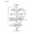
- FIG. 3 is a flowchart showing a routine for generating shot data according to an embodiment of the present invention.
- FIG. 4 is a conceptual diagram showing a routine for generating shot data according to an embodiment of the present invention.
- FIG. 5A to 5C is conceptual diagram explaining of a method of distributing of shot-divided graphic to subfield area.
- FIGS. 6A and 6B are conceptual diagrams explaining of a method of distributing of shot-divided graphic to subfield area.
- FIG. 7 is a conceptual diagram of distributing of graphic to subfield area in multi-pass writing.
- FIGS. 8A and 8B are conceptual diagram of explaining of effect on division of subfield.
- FIG. 9 is a conceptual diagram showing a configuration of an electron beam writing apparatus according to a second embodiment of the present invention.
- FIGS. 10A and 10B are diagrams of explaining of a positional shift of an electron beam produced on a sample 142 .
- FIG. 11 is a diagram of explaining of a conventional offset process.
- FIG. 12A and 12B are diagrams explaining a write data modifying process.
- FIG. 13 is a conceptual diagram of explaining of a conventional shot data generating method.
- FIG. 1 is a conceptual diagram showing a configuration of an electron beam writing apparatus according to a first embodiment of the present invention.
- the electron beam writing apparatus shown in FIG. 1 is equipped with a writing section 100 , which includes an electronic lens barrel 102 .
- An illuminating lens 114 for applying an electron beam (electron beam accelerated at 50 kV, for example) 112 emitted from an electron gun 110 to a first shaping aperture 120 is disposed within the electronic lens barrel 102 .
- the electron beam 112 is formed so as to assume a rectangle in its sectional shape by being penetrated through the first shaping aperture 120 having a rectangular opening.
- the so-shaped electron beam 112 is projected onto a second shaping aperture 126 by a projection lens 122 .
- a molding or shaping deflector 124 is disposed concentrically with the electronic lens barrel 102 between the second shaping aperture 126 and the first shaping aperture 120 . Since the degree of overlaying of a first shaping aperture image on an opening of the second shaping aperture 126 changes under control of the shaping deflector 124 , the shape and size of the electron beam 112 can be controlled.
- a focal point of the electron beam 112 transmitted through the second shaping aperture 126 is focused on the surface of a sample 142 lying within a writing chamber 104 by an objective lens 128 .
- the sample 142 is placed on an XY stage 140 continuously moved in an X direction (horizontal direction as viewed in the figure) and a Y direction (depth direction as viewed in the figure).
- the XY stage 140 is moved by a driver 230 and the amount of movement of the XY stage 140 is measured by a laser length measuring instrument 232 , so that its position can be recognized.
- the sample 142 is, for example, a reticle or a mask in which a light-shielding film such as a chromium film and a resist film are stacked or laminated on a glass substrate.
- a main deflector 130 and a sub deflector 132 each corresponding to an object deflector are disposed concentrically with the electronic lens barrel 102 between the sample 142 and the second shaping aperture 126 .
- a position where the electron beam 112 is applied onto the sample 142 is determined by the main deflector 130 and the sub deflector 132 .
- a pattern 11 to be written onto the sample 142 is divided into strip-like frame areas 12 as shown in FIG. 2 .
- the respective frame areas 12 are written while the XY stage 140 is being continuously moved in the X direction and/or Y direction.
- Each frame area 12 is further divided into a plurality of subfield areas 13 .
- the electron beam 112 shaped by the first and second shaping apertures 120 and 126 is deflected to write only a required part lying within the subfield area 13 .
- the writing process is performed for every strip-like stripe area (shown with being hatched in FIG. 2 ) Sr different from the frame area 12 .
- a two-stage object deflector comprised of the main deflector 130 and sub deflector 132 is used for deflection of the electron beam 112 .
- the positioning of the subfield area 13 is performed by the main deflector 130 , whereas the location of a pattern writing position within the subfield area 13 is performed by the sub deflector 132 .
- the electron beam writing apparatus shown in FIG. 1 is equipped with a control section 200 .
- the control section 200 is provided with a control computer 202 that performs various controls on the electron beam writing apparatus.
- the control computer 202 is connected with a storage device 204 , which stores design data (CAD data) therein.
- the design data are data obtained by converting chip data into formats capable of being inputted to the electron beam writing apparatus by an unillustrated external device.
- a write data converter 206 converts the design data read from the storage device 204 to write data of a format inside the electron beam writing apparatus. The shape and position of each graphic pattern are defined in the write data.
- the format conversion of the design data to the write data may be performed by the external device.
- the post-format conversion write data is inputted to a pre-processor 208 .
- the pre-processor 208 performs pre-processing such as a format check for the write data, an estimation of the number of shots, etc.
- the write data subjected to the pre-processing is inputted to a shot data generator 210 .
- the shot data generator 210 has shot dividing means 212 for dividing graphic data defined in the write data into graphics expressed in shot units, and distributing means 214 for distributing the respective graphics divided by the shot dividing means 212 to their corresponding subfield areas while performing a process for developing position information described in the write data.
- the shot dividing means 212 temporarily stores the graphics divided in the shot units into a memory 216 .
- the distributing means 214 reads each of the graphics stored in the memory 216 and distributes the read graphic to the subfield area.
- Shot data generated by the shot data generator 210 is inputted to a deflection controller 218 .
- the deflection controller 218 generates shaping deflection data for control of the shaping deflector 124 , main deflection data for control of the main deflector 130 and sub deflection data for control of the sub deflector 132 from the shot data.
- These shaping deflection data, main deflection data and sub deflection data are indication voltage signals of respective electrodes that configure the shaping deflector 124 , main deflector 130 and sub deflector 132 .
- the shaping deflection data generated at the deflection controller 218 is transmitted to a shaping deflection amplifier 220 , the main deflection data is transmitted to a main deflection amplifier 222 , and the sub deflection data is transmitted to a sub deflection amplifier 224 , respectively.
- the shaping deflection data, the main deflection data and the sub deflection data are respectively DA-converted by the shaping deflection amplifier 220 , the main deflection amplifier 222 and the sub deflection amplifier 224 .
- the DA-converted signals are respectively amplified to be capable of driving the respective electrodes and then applied to the shaping deflector 124 , the main deflector 130 and the sub deflector 132 .
- the writing process is executed.
- a shot data generating method corresponding to a characterizing portion of the present invention will next be explained with reference to FIGS. 3 through 7 .
- FIG. 3 is a flowchart showing a routine for generating shot data.
- the routine is started up by the shot data generator 210 .
- Step S 10 it is discriminated whether a graphic pattern defined in an inputted write pattern has already been shot-divided at a previous pass. It is discriminated at Step S 10 whether the inputted graphic pattern is identical to the graphic pattern shot-divided at the previous pass.
- Step S 10 When it is determined at Step S 10 referred to above that the graphic pattern has already been shot-divided at the previous pass (first pass), the routine proceeds to a process of Step S 30 without executing a process of Step S 20 .
- the post-shot division graphics corresponding to the first pass stored in the memory 216 are used for processing of the following Step S 30 subsequent to a second pass.
- Step S 10 when it is discriminated at Step S 10 that the inputted graphic pattern is different from the graphic pattern shot-divided at the previous pass, i.e., when this time corresponds to shot division of a graphic pattern corresponding to the first time (first pass), the routine proceeds to the process of Step S 20 .
- the graphic pattern defined in the write data is divided into a plurality of graphics expressed in shot units.
- the divided graphics are stored in the memory 216 .
- the shot dividing method can be simplified. That is, if the graphic pattern of the same shape is taken, the division of graphics is done by a unique method.
- Step S 30 the respective graphics shot-divided at Step S 20 referred to above are read from the memory 216 while a process for developing position information defined in a state of being compressed to write data is being performed, and then distributed to their corresponding subfield areas (Step S 30 ).
- the respective graphics shot-divided at the first pass can be used after the second pass.
- distributions of graphics to subfield areas are rendered different from each other at first and second passes.
- subfield areas adjacent to one another are overlaid on one another by widths each greater than or equal to the maximum shot size as shown in FIG. 5A .
- An area hatched in FIG. 5A corresponds to one subfield area SF located in the center.
- the subfield area SF is superimposed on its adjacent each subfield area SF by the width of the maximum shot size a.
- the subfield areas SF are overlaid on each other in this way, so that the shot-divided graphics are always held within any one of the subfield areas.
- the width at which the subfield areas overlap each other is suitable for being set to the maximum shot size a in terms of the efficiency of the writing process.
- the standard part S at the distribution of each graphic FG to the corresponding subfield area SF may be set to the corner other than the lower left corner.
- the graphics may be distributed to any one of subfield areas SF, based on the positions of the standard parts S.
- the overlay width of each subfield area SF is assumed to be a length equal to 4/3a times the maximum shot size a, and a line that separates its overlaid region into half is assumed to be a shot determination line L.
- graphics FG are distributed to either a subfield area SFa or SFb depending on whether the centers of gravity corresponding to standard parts S of the graphics FG are located on any subfield area side as viewed from the shot determination line L.
- Step S 40 It is next discriminated whether processing corresponding to one stripe has been ended.
- the routine returns to the process of Step S 10 .
- the present routine is ended when the processing corresponding to one stripe is determined to have been ended.
- graphics shot-divided correspondingly are stored in the memory 216 .
- the graphic data defined in the write data is divided into the plural graphics expressed in the shot units, and thereafter the divided graphics are distributed to their corresponding subfield areas, thereby generating the shot data. Accordingly, the shot dividing method can be simplified as compared with the conventional method that performs the subfield division before the shot division.
- the conventional method that performs the subfield division before the shot division is accompanied by a problem in that when the boundary (referred to as “subfieldboundary” hereinafter) B between subfield areas exists as shown in FIG. 8A , the number of shots increases in a region R close to the subfield boundary B.
- the number of shots is constant regardless of the presence or absence of subfield boundaries B as shown in FIG. 8B , and hence the number of shots can be prevented from increasing.
- the shot dividing method simplified in this way can be adopted upon execution of an estimation of the number of shots for pre-processing, it is possible to enhance the accuracy of an estimation of the number of shots conducted at the pre-processor 208 , by extension, the accuracy of an estimation of a writing time.
- the graphics shot-divided at the first pass are read from the memory 216 and used upon the distribution of the graphics to the subfield areas after the second pass, thereby making unnecessary the shot division subsequent to the second pass.
- the time necessary for the shot division after the second pass can be reduced, the time taken to generate shot data can be shortened. It is thus possible to improve writing throughput.
- the graphics shot-divided upon the generation of the shot data at the first pass are used for immediately-executed distribution to the subfield area at the second pass, thereby making it possible to erase the graphics stored in the memory 216 in a short time.
- FIG. 9 is a conceptual diagram showing a configuration of an electron beam writing apparatus according to the second embodiment of the present invention.
- the electron beam writing apparatus shown in FIG. 9 is different from the electron beam writing apparatus shown in FIG. 1 in that a shot data generator 210 A further includes write data modifying means 213 in addition to shot dividing means 212 and distributing means 214 . Since the electron beam writing apparatus shown in FIG. 9 is similar in other configuration to the electron beam writing apparatus shown in FIG. 1 , the detailed description thereof will be omitted.
- the write data modifying means 213 performs a write data modifying process for causing the positions of respective graphics divided by the shot dividing means 212 to be moved on write data.
- the distributing means 214 distributes the respective graphics to their corresponding subfield areas, based on the positions of the graphics moved on the write data by the write data modifying means 213 .
- the write data modifying process executed by the write data modifying means 213 will be explained with reference to FIGS. 10 through 12 .
- FIG. 10A A positional shift of an electron beam produced on a sample 142 of the electron beam writing apparatus will first be explained with reference to FIG. 10 .
- a position indicated by O is set as a reference point.
- an electron beam penetrated through a square opening of a first shaping aperture 120 is not deflected by a shaping deflector 124 , it assumes an electron beam having an approximately square horizontal sectional shape and penetrates an opening 126 a of a second shaping aperture 126 .
- An approximately square pattern Pa is written in a predetermined position on the sample 142 shown in FIG. 10B by the electron beam 112 a 1 transmitted through the opening 126 a.
- the electron beam penetrated through the opening of the first shaping aperture 120 is deflected by ⁇ x 1 to the plus side (right side in the figure) of an X axis and deflected by ⁇ y 1 to the plus side (upper side in the figure) of a Y axis by the shaping deflector 124 , it assumes an electron beam having an approximately triangular horizontal sectional shape and penetrates an upper right portion 126 a 1 of the opening 126 a of the second shaping aperture 126 .
- an approximately triangular pattern Pb is written in a position shifted by ⁇ x 1 ′ from the position of the rectangular pattern Pa to the plus side of the X axis on the sample 142 and shifted by ⁇ y 1 ′ from the position thereof to the plus side of the Y axis on the sample 142 .
- an approximately triangular pattern Pc is written in a position shifted by ⁇ x 2 ′ from the position of the rectangular pattern Pa to the minus side of the X axis on the sample 142 and shifted by ⁇ y 2 ′ from the position thereof to the plus side of the Y axis on the sample 142 .
- Other patterns Pd and Pe are also written in their corresponding positions shifted from the position of the rectangular pattern Pa on the sample 142 .
- the electron beam is deflected to the minus side of the X-axis and the minus side of the Y axis by the sub deflector 132 as indicated by arrow in FIG. 11 .
- a pattern Pb′ is written in a target position (i.e., a position where the positional shifts ⁇ x 1 ′ and ⁇ y 1 ′ are canceled out) on the sample 142 .
- a write data modifying process is performed without carrying out the conventional offset process.
- a description will be made of an example in which approximately triangular patterns Pb 1 , Pb 2 , Pb 3 and Pb 4 located at the four corners of a critical area Aam shown in FIG. 12A are written.
- arrows shown in FIG. 12A respectively indicate positional shifts of an electron beam caused by its penetration portion of the second shaping aperture.
- the positional shift ⁇ x 1 ′ in the X-axis direction and the positional shift ⁇ y 1 ′ in the Y-axis direction occur in the pattern Pb written by the electron beam 112 a 1 .
- the write data modifying process for canceling out the positional shifts of these patterns Pb 1 , Pb 2 , Pb 3 and Pb 4 is performed by the write data modifying means 213 . That is, the respective graphics subjected to the shot division are moved to the minus side of the X axis by the amount corresponding to the positional shift ⁇ x 1 ′ in the X-axis direction and moved to the minus side of the Y axis by the amount corresponding to the positional shift ⁇ y 1 ′ in the Y-axis direction on the write data.
- shot-divided graphics FGb 1 , FGb 2 , FGb 3 and FGb 4 are moved to their corresponding positions of graphics FGb 1 ′, FGb 2 ′, FGb 3 ′ and FGb 4 ′ on write data.
- a plurality of graphics FGb 1 ′, FGb 2 ′, FGb 3 ′ and FGb 4 ′ contained in write data are respectively distributed to any of plural subfields by the distributing means 214 .
- a graphic FGb 1 ′ is distributed to its corresponding subfield SFm
- a graphic FGb 2 ′ is distributed to its corresponding subfield SF 1
- a graphic FGb 3 ′ is distributed to its corresponding subfield SF 1 - 1
- a graphic FGb 4 ′ is distributed to its corresponding subfield SFm- 1 .
- the size of the subfield can be made identical to the size of the critical area (Aam) as shown in FIG. 12 . That is, it is not necessary to set the size of the subfield smaller than the size of the critical area.
- the present invention is not limited to the above embodiments, but may be implemented by making various modifications thereto within the scope not departing from the gist of the present invention.
- the electron beam has been used in the above embodiments, for example, the present invention is not limited to it.
- the present invention is applicable even to the case where other charged particle beams such as an ion beam, etc. are used.
- the distribution of each graphic to the subfield area is performed after the shot division while the development process of each pattern position is being performed, the shot division may be carried out while performing the development process of each pattern position.
- each graphic pattern defined in write data is divided into a plurality of graphics expressed in shot units by shot dividing means.
- the divided graphics are distributed to their corresponding subfield areas by distributing means.
- each graphic pattern of write data is divided into a plurality of graphics expressed in shot units.
- the divided graphics are distributed to their corresponding subfield areas.
- shot division can be simplified.
- the number of shots can be prevented from increasing and the time necessary to generate shot data can be shortened, writing throughput can be improved.
- the shot division can be shared between a plurality of passes by applying the present invention to a case in which each pattern is written by multi-pass writing. Namely, since there is no need to perform the shot division by the number of passes and the shot division may be performed once, writing throughput can be enhanced.
Landscapes
- Engineering & Computer Science (AREA)
- Chemical & Material Sciences (AREA)
- Nanotechnology (AREA)
- Physics & Mathematics (AREA)
- General Physics & Mathematics (AREA)
- Analytical Chemistry (AREA)
- Crystallography & Structural Chemistry (AREA)
- Mathematical Physics (AREA)
- Theoretical Computer Science (AREA)
- Plasma & Fusion (AREA)
- Condensed Matter Physics & Semiconductors (AREA)
- Manufacturing & Machinery (AREA)
- Electron Beam Exposure (AREA)
- Exposure And Positioning Against Photoresist Photosensitive Materials (AREA)
Abstract
Description
Claims (6)
Applications Claiming Priority (2)
| Application Number | Priority Date | Filing Date | Title |
|---|---|---|---|
| JP2008-240340 | 2008-09-19 | ||
| JP2008240340A JP5243898B2 (en) | 2008-09-19 | 2008-09-19 | Charged particle beam drawing apparatus and charged particle beam drawing method |
Publications (2)
| Publication Number | Publication Date |
|---|---|
| US20100072390A1 US20100072390A1 (en) | 2010-03-25 |
| US8669537B2 true US8669537B2 (en) | 2014-03-11 |
Family
ID=42036678
Family Applications (1)
| Application Number | Title | Priority Date | Filing Date |
|---|---|---|---|
| US12/560,802 Active 2031-07-08 US8669537B2 (en) | 2008-09-19 | 2009-09-16 | Charged particle beam writing apparatus and method |
Country Status (2)
| Country | Link |
|---|---|
| US (1) | US8669537B2 (en) |
| JP (1) | JP5243898B2 (en) |
Cited By (2)
| Publication number | Priority date | Publication date | Assignee | Title |
|---|---|---|---|---|
| US20160300687A1 (en) * | 2015-04-10 | 2016-10-13 | Nuflare Technology, Inc. | Charged particle beam writing apparatus and charged particle beam writing method |
| US20180366297A1 (en) * | 2017-06-14 | 2018-12-20 | Nuflare Technology, Inc. | Data processing method, charged particle beam writing apparatus, and charged particle beam writing system |
Families Citing this family (13)
| Publication number | Priority date | Publication date | Assignee | Title |
|---|---|---|---|---|
| JP5547553B2 (en) | 2010-05-26 | 2014-07-16 | 株式会社ニューフレアテクノロジー | Charged particle beam drawing apparatus and control method thereof |
| JP5547567B2 (en) | 2010-06-30 | 2014-07-16 | 株式会社ニューフレアテクノロジー | Charged particle beam drawing apparatus and control method thereof |
| JP5636238B2 (en) | 2010-09-22 | 2014-12-03 | 株式会社ニューフレアテクノロジー | Charged particle beam drawing apparatus and charged particle beam drawing method |
| JP5662756B2 (en) * | 2010-10-08 | 2015-02-04 | 株式会社ニューフレアテクノロジー | Charged particle beam drawing apparatus and charged particle beam drawing method |
| JP5601989B2 (en) | 2010-11-19 | 2014-10-08 | 株式会社ニューフレアテクノロジー | Charged particle beam drawing apparatus and charged particle beam drawing method |
| JP5809419B2 (en) | 2011-02-18 | 2015-11-10 | 株式会社ニューフレアテクノロジー | Charged particle beam drawing apparatus and charged particle beam drawing method |
| JP2012253316A (en) * | 2011-05-12 | 2012-12-20 | Nuflare Technology Inc | Charged particle beam lithography apparatus and charged particle beam lithography method |
| JP2013045838A (en) * | 2011-08-23 | 2013-03-04 | Canon Inc | Drawing device and manufacturing method of article |
| US8745549B2 (en) * | 2012-02-05 | 2014-06-03 | D2S, Inc. | Method and system for forming high precision patterns using charged particle beam lithography |
| JP5985852B2 (en) | 2012-03-27 | 2016-09-06 | 株式会社ニューフレアテクノロジー | Charged particle beam drawing apparatus and charged particle beam drawing method |
| JP6353278B2 (en) | 2014-06-03 | 2018-07-04 | 株式会社ニューフレアテクノロジー | Multi-charged particle beam writing method and multi-charged particle beam writing apparatus |
| JP2016184605A (en) * | 2015-03-25 | 2016-10-20 | 株式会社ニューフレアテクノロジー | Charged particle beam drawing device and drawing date creation method |
| JP6901374B2 (en) * | 2017-10-10 | 2021-07-14 | 日本電子株式会社 | Charged particle beam drawing device |
Citations (18)
| Publication number | Priority date | Publication date | Assignee | Title |
|---|---|---|---|---|
| US5189306A (en) * | 1992-03-24 | 1993-02-23 | International Business Machines Corporation | Grey-splice algorithm for electron beam lithography post-processor |
| US5523580A (en) * | 1993-12-23 | 1996-06-04 | International Business Machines Corporation | Reticle having a number of subfields |
| US6015975A (en) * | 1997-04-10 | 2000-01-18 | Fujitsu Limited | Method and apparatus for charged particle beam exposure |
| US6194102B1 (en) * | 1998-01-14 | 2001-02-27 | Nikon Corporation | Pattern-transfer methods and masks |
| US6258511B1 (en) * | 1998-10-14 | 2001-07-10 | Nikon Corporation | Charged particle beam exposure method utilizing partial exposure stitch area |
| US6307209B1 (en) * | 1997-12-03 | 2001-10-23 | Nikon Corporation | Pattern-transfer method and apparatus |
| US6313476B1 (en) * | 1998-12-14 | 2001-11-06 | Kabushiki Kaisha Toshiba | Charged beam lithography system |
| US6333138B1 (en) * | 1999-03-08 | 2001-12-25 | Kabushiki Kaisha Toshiba | Exposure method utilizing partial exposure stitch area |
| US20020028398A1 (en) * | 2000-09-01 | 2002-03-07 | Kozo Ogino | Charged particle beam exposure method and charged particle beam exposure apparatus |
| US20040011966A1 (en) * | 2002-05-24 | 2004-01-22 | Noriaki Sasaki | Energy beam exposure method and exposure apparatus |
| US20040079896A1 (en) * | 2002-10-29 | 2004-04-29 | International Business Machines Corporation | Method and structure for detection of electromechanical problems using variance statistics in an E-beam lithography device |
| US6774380B2 (en) * | 2001-09-28 | 2004-08-10 | Kabushiki Kaisha Toshiba | Variably shaped beam EB writing system |
| US20080067426A1 (en) * | 2006-05-30 | 2008-03-20 | Nuflare Technology, Inc. | Pattern writing circuit self-diagnosis method for charged beam photolithography apparatus and charged beam photolithography apparatus |
| US20080067423A1 (en) * | 2006-05-30 | 2008-03-20 | Nuflare Technology, Inc. | Writing error diagnosis method for charged particle beam photolithography apparatus and charged particle beam photolithography apparatus |
| JP2008117820A (en) | 2006-10-31 | 2008-05-22 | Toshiba Corp | Electron beam drawing data creation method, creation apparatus, creation program, and electron beam drawing apparatus |
| JP2008182073A (en) | 2007-01-25 | 2008-08-07 | Nuflare Technology Inc | Charged particle beam lithography system |
| US20090134343A1 (en) * | 2007-11-26 | 2009-05-28 | Nuflare Technology, Inc. | Tracking control method and electron beam writing system |
| US8122390B2 (en) * | 2008-02-13 | 2012-02-21 | Nuflare Technology, Inc. | Charged particle beam writing apparatus, and apparatus and method for correcting dimension error of pattern |
Family Cites Families (3)
| Publication number | Priority date | Publication date | Assignee | Title |
|---|---|---|---|---|
| JP3469422B2 (en) * | 1996-02-23 | 2003-11-25 | 株式会社東芝 | Charged beam writing method and writing apparatus |
| JP3612166B2 (en) * | 1997-03-18 | 2005-01-19 | 株式会社東芝 | Charged beam drawing data creation method and apparatus |
| JP2005072055A (en) * | 2003-08-27 | 2005-03-17 | Toshiba Mach Co Ltd | Charged beam drawing method, charged beam drawing apparatus, drawing data creation method, and drawing control program |
-
2008
- 2008-09-19 JP JP2008240340A patent/JP5243898B2/en active Active
-
2009
- 2009-09-16 US US12/560,802 patent/US8669537B2/en active Active
Patent Citations (19)
| Publication number | Priority date | Publication date | Assignee | Title |
|---|---|---|---|---|
| US5189306A (en) * | 1992-03-24 | 1993-02-23 | International Business Machines Corporation | Grey-splice algorithm for electron beam lithography post-processor |
| US5523580A (en) * | 1993-12-23 | 1996-06-04 | International Business Machines Corporation | Reticle having a number of subfields |
| US6015975A (en) * | 1997-04-10 | 2000-01-18 | Fujitsu Limited | Method and apparatus for charged particle beam exposure |
| US6307209B1 (en) * | 1997-12-03 | 2001-10-23 | Nikon Corporation | Pattern-transfer method and apparatus |
| US6194102B1 (en) * | 1998-01-14 | 2001-02-27 | Nikon Corporation | Pattern-transfer methods and masks |
| US6258511B1 (en) * | 1998-10-14 | 2001-07-10 | Nikon Corporation | Charged particle beam exposure method utilizing partial exposure stitch area |
| US6313476B1 (en) * | 1998-12-14 | 2001-11-06 | Kabushiki Kaisha Toshiba | Charged beam lithography system |
| US6333138B1 (en) * | 1999-03-08 | 2001-12-25 | Kabushiki Kaisha Toshiba | Exposure method utilizing partial exposure stitch area |
| US20020028398A1 (en) * | 2000-09-01 | 2002-03-07 | Kozo Ogino | Charged particle beam exposure method and charged particle beam exposure apparatus |
| US6774380B2 (en) * | 2001-09-28 | 2004-08-10 | Kabushiki Kaisha Toshiba | Variably shaped beam EB writing system |
| US20060060800A1 (en) * | 2001-09-28 | 2006-03-23 | Takayuki Abe | Variably shaped beam EB writing system |
| US20040011966A1 (en) * | 2002-05-24 | 2004-01-22 | Noriaki Sasaki | Energy beam exposure method and exposure apparatus |
| US20040079896A1 (en) * | 2002-10-29 | 2004-04-29 | International Business Machines Corporation | Method and structure for detection of electromechanical problems using variance statistics in an E-beam lithography device |
| US20080067426A1 (en) * | 2006-05-30 | 2008-03-20 | Nuflare Technology, Inc. | Pattern writing circuit self-diagnosis method for charged beam photolithography apparatus and charged beam photolithography apparatus |
| US20080067423A1 (en) * | 2006-05-30 | 2008-03-20 | Nuflare Technology, Inc. | Writing error diagnosis method for charged particle beam photolithography apparatus and charged particle beam photolithography apparatus |
| JP2008117820A (en) | 2006-10-31 | 2008-05-22 | Toshiba Corp | Electron beam drawing data creation method, creation apparatus, creation program, and electron beam drawing apparatus |
| JP2008182073A (en) | 2007-01-25 | 2008-08-07 | Nuflare Technology Inc | Charged particle beam lithography system |
| US20090134343A1 (en) * | 2007-11-26 | 2009-05-28 | Nuflare Technology, Inc. | Tracking control method and electron beam writing system |
| US8122390B2 (en) * | 2008-02-13 | 2012-02-21 | Nuflare Technology, Inc. | Charged particle beam writing apparatus, and apparatus and method for correcting dimension error of pattern |
Non-Patent Citations (4)
| Title |
|---|
| Office Action issued in Japanese Application No. 2008-240340 filed Sep. 19, 2008 (w/English translation). |
| U.S. Appl. No. 13/235,432, filed Sep. 18, 2011, Nakayamada, et al. |
| U.S. Appl. No. 13/288,530, filed Nov. 3, 2011, Yashima. |
| U.S. Appl. No. 13/765,140, filed Feb. 12, 2013, Kato, et al. |
Cited By (4)
| Publication number | Priority date | Publication date | Assignee | Title |
|---|---|---|---|---|
| US20160300687A1 (en) * | 2015-04-10 | 2016-10-13 | Nuflare Technology, Inc. | Charged particle beam writing apparatus and charged particle beam writing method |
| US9734981B2 (en) * | 2015-04-10 | 2017-08-15 | Nuflare Technology, Inc. | Charged particle beam writing apparatus and charged particle beam writing method |
| US20180366297A1 (en) * | 2017-06-14 | 2018-12-20 | Nuflare Technology, Inc. | Data processing method, charged particle beam writing apparatus, and charged particle beam writing system |
| US10714312B2 (en) * | 2017-06-14 | 2020-07-14 | Nuflare Technology, Inc. | Data processing method, charged particle beam writing apparatus, and charged particle beam writing system |
Also Published As
| Publication number | Publication date |
|---|---|
| US20100072390A1 (en) | 2010-03-25 |
| JP2010073918A (en) | 2010-04-02 |
| JP5243898B2 (en) | 2013-07-24 |
Similar Documents
| Publication | Publication Date | Title |
|---|---|---|
| US8669537B2 (en) | Charged particle beam writing apparatus and method | |
| KR100914116B1 (en) | Charged particle beam writing apparatus and charged particle beam writing method | |
| US6222195B1 (en) | Charged-particle-beam exposure device and charged-particle-beam exposure method | |
| KR101006676B1 (en) | Charged Particle Beam Writing Apparatus and Charged Particle Beam Writing Method | |
| US8122390B2 (en) | Charged particle beam writing apparatus, and apparatus and method for correcting dimension error of pattern | |
| US7863586B2 (en) | Writing data creation method and charged particle beam writing apparatus | |
| US8878149B2 (en) | Charged particle beam writing apparatus and charged particle beam writing method | |
| US8779379B2 (en) | Acquisition method of charged particle beam deflection shape error and charged particle beam writing method | |
| US11789372B2 (en) | Writing data generating method and multi charged particle beam writing apparatus | |
| US9548183B2 (en) | Charged particle beam writing apparatus, and charged particle beam writing method | |
| US20220100099A1 (en) | Writing data generating method, multi charged particle beam writing apparatus, pattern inspecting apparatus, and computer-readable recording medium | |
| US8431908B2 (en) | Charged particle beam writing apparatus and charged particle beam writing method | |
| USRE47707E1 (en) | Charged particle beam writing apparatus and charged particle beam writing method | |
| US9484185B2 (en) | Charged particle beam writing apparatus, and charged particle beam writing method | |
| US20080265174A1 (en) | Charged particle beam writing apparatus and method | |
| US8423921B2 (en) | Data verification method and charged particle beam writing apparatus | |
| JP6171062B2 (en) | Charged particle beam drawing apparatus and charged particle beam drawing method | |
| JP5174531B2 (en) | Charged particle beam drawing apparatus and drawing method in charged particle beam drawing apparatus | |
| US7582884B2 (en) | Charged particle beam exposure method and charged particle beam exposure device | |
| JP2010147066A (en) | Coordinate measuring apparatus and charged particle beam drawing equipment | |
| JPH11329933A (en) | Charged particle beam exposure system | |
| JP2017228650A (en) | Charged particle beam lithography apparatus and charged particle beam lithography method | |
| JP2008016541A (en) | Electron beam drawing apparatus, electron beam drawing method, and control program | |
| JPH01251718A (en) | Charged beam lithography | |
| JPH05234861A (en) | Charged particle beam exposure method |
Legal Events
| Date | Code | Title | Description |
|---|---|---|---|
| AS | Assignment |
Owner name: NUFLARE TECHNOLOGY, INC.,JAPAN Free format text: ASSIGNMENT OF ASSIGNORS INTEREST;ASSIGNOR:YASHIMA, JUN;REEL/FRAME:023248/0907 Effective date: 20090904 Owner name: NUFLARE TECHNOLOGY, INC., JAPAN Free format text: ASSIGNMENT OF ASSIGNORS INTEREST;ASSIGNOR:YASHIMA, JUN;REEL/FRAME:023248/0907 Effective date: 20090904 |
|
| STCF | Information on status: patent grant |
Free format text: PATENTED CASE |
|
| FEPP | Fee payment procedure |
Free format text: PAYOR NUMBER ASSIGNED (ORIGINAL EVENT CODE: ASPN); ENTITY STATUS OF PATENT OWNER: LARGE ENTITY |
|
| MAFP | Maintenance fee payment |
Free format text: PAYMENT OF MAINTENANCE FEE, 4TH YEAR, LARGE ENTITY (ORIGINAL EVENT CODE: M1551) Year of fee payment: 4 |
|
| MAFP | Maintenance fee payment |
Free format text: PAYMENT OF MAINTENANCE FEE, 8TH YEAR, LARGE ENTITY (ORIGINAL EVENT CODE: M1552); ENTITY STATUS OF PATENT OWNER: LARGE ENTITY Year of fee payment: 8 |
|
| MAFP | Maintenance fee payment |
Free format text: PAYMENT OF MAINTENANCE FEE, 12TH YEAR, LARGE ENTITY (ORIGINAL EVENT CODE: M1553); ENTITY STATUS OF PATENT OWNER: LARGE ENTITY Year of fee payment: 12 |