US8648324B2 - Glassy carbon nanostructures - Google Patents
Glassy carbon nanostructures Download PDFInfo
- Publication number
- US8648324B2 US8648324B2 US12/727,710 US72771010A US8648324B2 US 8648324 B2 US8648324 B2 US 8648324B2 US 72771010 A US72771010 A US 72771010A US 8648324 B2 US8648324 B2 US 8648324B2
- Authority
- US
- United States
- Prior art keywords
- glassy carbon
- ridges
- additional material
- block copolymer
- electrical connection
- Prior art date
- Legal status (The legal status is an assumption and is not a legal conclusion. Google has not performed a legal analysis and makes no representation as to the accuracy of the status listed.)
- Active, expires
Links
Images


Classifications
-
- H—ELECTRICITY
- H01—ELECTRIC ELEMENTS
- H01G—CAPACITORS; CAPACITORS, RECTIFIERS, DETECTORS, SWITCHING DEVICES OR LIGHT-SENSITIVE DEVICES, OF THE ELECTROLYTIC TYPE
- H01G11/00—Hybrid capacitors, i.e. capacitors having different positive and negative electrodes; Electric double-layer [EDL] capacitors; Processes for the manufacture thereof or of parts thereof
- H01G11/22—Electrodes
- H01G11/26—Electrodes characterised by their structure, e.g. multi-layered, porosity or surface features
-
- B—PERFORMING OPERATIONS; TRANSPORTING
- B82—NANOTECHNOLOGY
- B82Y—SPECIFIC USES OR APPLICATIONS OF NANOSTRUCTURES; MEASUREMENT OR ANALYSIS OF NANOSTRUCTURES; MANUFACTURE OR TREATMENT OF NANOSTRUCTURES
- B82Y30/00—Nanotechnology for materials or surface science, e.g. nanocomposites
-
- B—PERFORMING OPERATIONS; TRANSPORTING
- B82—NANOTECHNOLOGY
- B82Y—SPECIFIC USES OR APPLICATIONS OF NANOSTRUCTURES; MEASUREMENT OR ANALYSIS OF NANOSTRUCTURES; MANUFACTURE OR TREATMENT OF NANOSTRUCTURES
- B82Y40/00—Manufacture or treatment of nanostructures
-
- H—ELECTRICITY
- H01—ELECTRIC ELEMENTS
- H01G—CAPACITORS; CAPACITORS, RECTIFIERS, DETECTORS, SWITCHING DEVICES OR LIGHT-SENSITIVE DEVICES, OF THE ELECTROLYTIC TYPE
- H01G11/00—Hybrid capacitors, i.e. capacitors having different positive and negative electrodes; Electric double-layer [EDL] capacitors; Processes for the manufacture thereof or of parts thereof
- H01G11/22—Electrodes
- H01G11/30—Electrodes characterised by their material
- H01G11/32—Carbon-based
- H01G11/36—Nanostructures, e.g. nanofibres, nanotubes or fullerenes
-
- H—ELECTRICITY
- H01—ELECTRIC ELEMENTS
- H01G—CAPACITORS; CAPACITORS, RECTIFIERS, DETECTORS, SWITCHING DEVICES OR LIGHT-SENSITIVE DEVICES, OF THE ELECTROLYTIC TYPE
- H01G11/00—Hybrid capacitors, i.e. capacitors having different positive and negative electrodes; Electric double-layer [EDL] capacitors; Processes for the manufacture thereof or of parts thereof
- H01G11/22—Electrodes
- H01G11/30—Electrodes characterised by their material
- H01G11/46—Metal oxides
-
- H—ELECTRICITY
- H01—ELECTRIC ELEMENTS
- H01M—PROCESSES OR MEANS, e.g. BATTERIES, FOR THE DIRECT CONVERSION OF CHEMICAL ENERGY INTO ELECTRICAL ENERGY
- H01M4/00—Electrodes
- H01M4/02—Electrodes composed of, or comprising, active material
- H01M4/62—Selection of inactive substances as ingredients for active masses, e.g. binders, fillers
- H01M4/624—Electric conductive fillers
- H01M4/625—Carbon or graphite
-
- H—ELECTRICITY
- H01—ELECTRIC ELEMENTS
- H01M—PROCESSES OR MEANS, e.g. BATTERIES, FOR THE DIRECT CONVERSION OF CHEMICAL ENERGY INTO ELECTRICAL ENERGY
- H01M10/00—Secondary cells; Manufacture thereof
- H01M10/05—Accumulators with non-aqueous electrolyte
- H01M10/052—Li-accumulators
- H01M10/0525—Rocking-chair batteries, i.e. batteries with lithium insertion or intercalation in both electrodes; Lithium-ion batteries
-
- Y—GENERAL TAGGING OF NEW TECHNOLOGICAL DEVELOPMENTS; GENERAL TAGGING OF CROSS-SECTIONAL TECHNOLOGIES SPANNING OVER SEVERAL SECTIONS OF THE IPC; TECHNICAL SUBJECTS COVERED BY FORMER USPC CROSS-REFERENCE ART COLLECTIONS [XRACs] AND DIGESTS
- Y02—TECHNOLOGIES OR APPLICATIONS FOR MITIGATION OR ADAPTATION AGAINST CLIMATE CHANGE
- Y02E—REDUCTION OF GREENHOUSE GAS [GHG] EMISSIONS, RELATED TO ENERGY GENERATION, TRANSMISSION OR DISTRIBUTION
- Y02E60/00—Enabling technologies; Technologies with a potential or indirect contribution to GHG emissions mitigation
- Y02E60/10—Energy storage using batteries
-
- Y—GENERAL TAGGING OF NEW TECHNOLOGICAL DEVELOPMENTS; GENERAL TAGGING OF CROSS-SECTIONAL TECHNOLOGIES SPANNING OVER SEVERAL SECTIONS OF THE IPC; TECHNICAL SUBJECTS COVERED BY FORMER USPC CROSS-REFERENCE ART COLLECTIONS [XRACs] AND DIGESTS
- Y02—TECHNOLOGIES OR APPLICATIONS FOR MITIGATION OR ADAPTATION AGAINST CLIMATE CHANGE
- Y02E—REDUCTION OF GREENHOUSE GAS [GHG] EMISSIONS, RELATED TO ENERGY GENERATION, TRANSMISSION OR DISTRIBUTION
- Y02E60/00—Enabling technologies; Technologies with a potential or indirect contribution to GHG emissions mitigation
- Y02E60/13—Energy storage using capacitors
Definitions
- the invention relates to glassy carbon structures, and more particularly, to glassy carbon nanostructures suitable for use in batteries, electrochemical capacitors, and photocatalytic devices, for example.
- Glassy carbon materials, semiconductor-glassy carbon composite materials, and metal oxide-glassy carbon composite materials are disclosed herein that can be used as an electrode in an electrochemical capacitor or in a battery (e.g., in a Li ion battery), or as a photoelectrode in photocatalysis or photoelectrochemistry devices. Associated methods are disclosed that lead to the formation of materials whose features can be controlled over a large area.
- channels e.g., substantially cylindrically-shaped pores, which are preferably non-interconnected
- ridges are formed that extend along and over a glassy carbon substrate. With either the channel or the ridge embodiments, a semiconductor and/or metal oxide may be deposited over the glassy carbon to form a glassy carbon composite material.
- the channels and ridges may be advantageously formed by applying a solution (that contains a block copolymer) over a glassy carbon substrate. Following self-assembly of the block copolymer, one of its domains is removed, thereby leaving a polymeric structure that is then used as an etch mask. An etch process, such as an oxygen plasma etch, can be used to remove portions of the glassy carbon substrate. Depending upon the block copolymer used and its morphology, channels or ridges may be formed in the underlying glassy carbon substrate. These channels and ridges have dimensions that facilitate the efficient splitting of electron-hole pairs when they are in contact with a semiconductor layer.
- a semiconductor layer and/or metal oxide layer may be applied through any one of a number of techniques, such as spin coating, dip coating, drop casting, vacuum deposition, electroplating, and so on.
- the band gap of the semiconductor can be tuned by hybridizing one semiconductor material with one or more other materials.
- titanium dioxide (TiO 2 ) may be hybridized with semiconductor nanocrystals (such as quantum dots) and metal oxides.
- One preferred embodiment is a device that includes a first structure consisting essentially of glassy carbon, with the first structure having at least 1000 discrete channels extending into the first structure.
- the channels have i) a critical dimension (CD) between 5 and 70 nanometers; ii) an aspect ratio (depth/CD) of at least 1.0; and iii) an areal density of at least 10 10 /cm 2 .
- the channels are preferably substantially cylindrical.
- a semiconductor (other than carbon) and/or metal oxide is in contact with the channels, e.g., the semiconductor and/or metal oxide may fill the channels or it may form a conformal layer over the first structure (e.g., this layer may have a thickness of at least 1 nanometer).
- a semiconductor and/or metal oxide may be selected from the group consisting of titania, manganese oxide, tin oxide, and indium tin oxide.
- the first structure may be used in combination with another similar structure to form a battery, an electrochemical capacitor, or a photocatalytic device.
- Another preferred embodiment is a device that includes a first structure consisting essentially of glassy carbon, with the first structure having at least 1000 discrete ridges therein.
- the ridges have i) a width between 5 and 70 nanometers; ii) a height to width ratio of at least 1.0; iii) a length to width ratio of at least 3.0; and iv) a linear density of at least 10 5 /cm, as measured along a line segment passing through the ridges.
- a semiconductor (other than carbon) and/or metal oxide is in contact with the ridges, e.g., the semiconductor and/or metal oxide may form a conformal layer over the first structure (e.g., this layer may have a thickness of at least 1 nanometer). If a semiconductor and/or metal oxide is used, it may be selected from the group consisting of titania, manganese oxide, tin oxide, and indium tin oxide.
- the first structure may be used in combination with another similar structure to form a battery, an electrochemical capacitor, or a photocatalytic device.
- FIG. 1 is schematic of a glassy carbon structure, in which cylindrical channels extend beneath the surface of the structure;
- FIG. 2 shows the structure of FIG. 1 but with a semiconductor layer and/or metal oxide deposited over the glassy carbon;
- FIG. 3 is a schematic of a glassy carbon structure, in which ridges extend along a surface of the structure
- FIG. 4 shows the structure of FIG. 3 but with a semiconductor and/or metal oxide layer deposited over the glassy carbon;
- FIG. 5 shows how glassy carbon structures disclosed herein can be incorporated into a battery
- FIG. 6 shows how glassy carbon structures disclosed herein can be incorporated into an electrochemical capacitor
- FIG. 7 shows how glassy carbon structures disclosed herein can be incorporated into a photocatalytic device
- FIG. 8 and FIG. 9 which includes FIGS. 9A , 9 B, and 9 C, schematically illustrate a process for forming a glassy carbon structure having channels therein, such as the structure shown in FIG. 1 ;
- FIG. 10 schematically illustrates a process for forming a glassy carbon structure having ridges therein, such as the structure shown in FIG. 3 ;
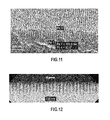
- FIG. 11 is a cross-sectional SEM image of a glassy carbon structure having channels therein;
- FIG. 12 is a cross-sectional TEM image of the structure shown in FIG. 11 ;
- FIG. 13 shows how the water contact angle on a glassy carbon wafer (left) differs from that on a glassy carbon surface into which channels have been introduced (right);
- FIG. 14 shows a cross-sectional TEM image of a titania-glassy carbon composite, in which titania has been deposited into and fills the channels of the glassy carbon;
- FIG. 15 shows an SEM image of a titania-glassy carbon composite prepared by electroplating titania onto glassy carbon having channels therein;
- FIG. 16 includes FIGS. 16A and 16B , in which:
- FIG. 16A is a schematic of a cell that includes a titania-glassy carbon composite.
- FIG. 16B shows how the current density of the cell changes upon exposure to UV light
- FIG. 17 shows tilted SEM micrographs of glassy carbon structures that include ridges.
- Preferred embodiments of the invention described herein include structures made of glassy carbon.
- Glassy carbon also known as vitreous or polymeric carbon
- Glassy carbon may be produced by the thermal degradation of a phenolic resin or furfuryl alcohol, for example.
- Glassy carbon is a non-graphitizing carbon, a carbon that cannot be transformed into crystalline graphite even at temperatures above 3000° C. It has relatively low electrical resistivity [ ⁇ (3-8) ⁇ 10 ⁇ 4 ⁇ cm], as well as relatively low density (1.5 g/cm 3 , compared to 2.26 g/cm 3 for graphite), with the latter being attributed to its significant volumetric pore fraction ( ⁇ 30% v/v). However, since these pores are “closed”, they do not contribute to the accessible surface area.
- the structures disclosed herein may include either channels or ridges that are formed in a substrate consisting essentially of glassy carbon (e.g., the substrate could be 100% or nearly 100% pure, e.g., >99% pure).
- These features which may have a characteristic dimension between 5 and 70 nm, effectively increase the surface area of the glassy carbon structure (in contrast with the “closed” pores described above, which do not increase the accessible surface area). This promotes better wettability with aqueous solutions and results in less pulverization of the structure as a result of any volume change that arises during ion insertion (e.g., Li ion insertion for Li-ion batteries).
- FIG. 1 shows a glassy carbon substrate 120 into which channels 130 have been formed.
- the channels 120 are preferably cylindrical in shape (although non-symmetrical cylindrical shapes such as ellipses are contemplated), or, for example, they may be conically shaped.
- the channels 120 may advantageously have a critical dimension between 5 and 70 nm, but more preferably between 5 and 50 nm.
- the channels 120 are cylindrically shaped, they preferably have a diameter between 5 and 70 nm, and more preferably between 5 and 50 nm.
- the depth of such channels may advantageously be between 5 and 250 or even 350 nm, with the aspect ratio (diameter/depth) of the channels preferably falling in the range of 1.0-5.0, and more preferably in the range of 1.0-3.0.
- the wall-to-wall separation between the channels may advantageously be between 2 and 30 nm.
- the channels may be partially or completely filled with a semiconductor and/or metal oxide material, e.g., a conformal layer 140 of semiconductor and/or metal oxide material may be deposited over the channels 130 , as shown in FIG. 2 .
- a semiconductor and/or metal oxide material e.g., a conformal layer 140 of semiconductor and/or metal oxide material may be deposited over the channels 130 , as shown in FIG. 2 .
- CVD chemical vapor deposition
- atomic layer deposition or a solution based process
- FIG. 3 shows another embodiment formed from glassy carbon material.
- ridges 330 are formed in a glassy carbon substrate 320 .
- the ridges 330 preferably have a width (measured at their base) in the range of 5-70 nm, and more preferably 5-50 nm.
- the height of the ridges 330 is preferably at least equal to their width, and the ridges may be separated from each other by 5-50 nm.
- the length of the ridges 330 is preferably at least 3 times their width, and more preferably at least 5 times their width.
- the length of the ridges 330 should be at least 15 nm; more preferably, their length is at least 100 nm or even 1000 nm or more.
- the ridges 330 are formed so that they are, at least in a given region, largely parallel to each other and substantially perpendicular to an axis 340 , although over larger regions this alignment will not necessarily be evident.
- the ridges 330 preferably have a linear density of 10 5 /cm-10 6 /cm.
- a layer 350 (e.g., a conformal layer) of semiconductor material and/or metal oxide material may be deposited over the ridges 330 , so that they are partially covered (e.g., just the peaks of the ridges may be covered) or they may be completely covered, as shown in the conformal layer example of FIG. 4 .
- FIG. 5 shows a battery 510 in which glassy-carbon based nanostructures (such as those shown in FIGS. 1 and/or 3 ) function as respective electrodes 520 , 530 separated by an electrolyte 540 .
- the electrolyte 540 may include a lithium salt (e.g., LiPF 6 ) in an aprotic organic solvent (such as propylene carbonate or ethylene carbonate).
- one (or both) of the electrodes of the battery 510 may include a semiconductor layer and/or metal oxide layer, as shown in FIGS. 2 and 4 .
- this semiconductor layer and/or metal oxide layer may include MnO 2 , a Si-based material, Al 2 O 3 , vanadium oxide, lithium oxide, cobalt oxide, and/or ruthenium oxide.
- FIG. 6 shows an electrochemical capacitor device 610 that is analogous in certain respects to the device shown in FIG. 5 .
- Two electrodes 620 , 630 made of glassy carbon nanostructures (such as those shown in FIGS. 1 and/or 3 ) are separated by an electrolyte 640 . If the electrolyte 640 is chosen properly, the device 610 functions as an electrochemical capacitor (e.g., H + and SO4 ⁇ may be used, or alternatively, K + and OH ⁇ ).
- an electrochemical capacitor e.g., H + and SO4 ⁇ may be used, or alternatively, K + and OH ⁇ ).
- FIG. 7 shows a photocatalytic device 710 .
- a glassy carbon nanostructure coated with a semiconductor layer functions as one electrode 720 , which is separated from a metal electrode 730 (e.g., made of platinum) by an aqueous solution 740 .
- a metal electrode 730 e.g., made of platinum
- an aqueous solution 740 e.g., water
- photons of the right wavelength are directed towards the electrode 720 , electron hole pairs are formed, leading to the formation of H 2 and O 2 as H 2 O is dissociated.
- a dye e.g., an organic dye
- This dye would be selected such that its absorbance spectrum matches the spectral distribution of the input photons, with the dye in turn reemitting photons at wavelengths favorable for producing electron-hole pairs in the semiconductor layer.
- Block copolymers are employed to form the carbon nanostructures disclosed herein. Additional details regarding these methods are described in the next section. Briefly, the blocks of such copolymers phase separate into microdomains (also known as “microphase-separated domains” or “domains”) to reduce the total free energy, and in the process, nanoscale features of dissimilar chemical composition are formed. Certain ones of these nanoscale features are then transferred via an etch process into an underlying substrate of glassy carbon.
- a surface energy control layer may be optionally used if there is a desire to control the orientation of the block copolymer microdomains.
- the surface energy control layer may include, for example, an organosilicate, such as polymethyl glutarimide (PMGI).
- a solution containing a block copolymer is applied on a substrate 820 of glassy carbon.
- the block copolymer (a block copolymer containing an organosilicate hybrid may also be used) may be spin-coated, for example, onto the surface of the glassy carbon substrate 820 .
- Microphase-separated domains 828 and 832 are then formed, e.g., as a result of an annealing process.
- FIG. 9A shows a cross sectional view of the substrate and the phase-separated block copolymer, as well as an optional surface energy control layer 840 , which may be used to pre-position the phase separated domains.
- an etch process e.g., an oxygen etch process
- the pitch of the pattern realized in the substrate 820 corresponds to that of the pitch in the lithographic pre-pattern.
- the domains 828 and any residue from the block copolymer are then removed (e.g., by rinsing with hydrofluoric acid), thereby leaving the desired nanostructure 860 , which is analogous to the structure shown in FIG. 1 .
- a semiconductor material and/or metal oxide material can be subsequently deposited on top of the nanoporous carbon surface.
- a wide band gap metal oxide like titania it may be deposited by electroplating or by depositing a titania precursor (e.g., by spin coating, dip coating, or drop casting a chelated sol-gel precursor).
- a titania precursor e.g., by spin coating, dip coating, or drop casting a chelated sol-gel precursor.
- the band gap of titania can be narrowed by blending the titania with other semiconductor nanocrystals, such as CdTe.
- lamellar forming block copolymers can also be used. After a suitable block copolymer-containing solution is cast over a glassy carbon substrate 1020 , self-assembly occurs leading to the formation of domains 1028 , 1032 that are aligned perpendicularly to the surface of the glassy carbon substrate. These perpendicularly oriented lamellae can be used to provide nanoscale line patterns in the substrate. A surface energy control layer (not shown) may be used to control the position of the domains 1028 , 1032 . In analogy with FIG. 9 , one of the domains can be selectively removed through an etching process, so that further etching into the substrate 1020 results in a series of ridges in the substrate, like the embodiment shown in FIG. 3 .
- the carbon nanostructures and the semiconductor-carbon composites (and/or metal oxide carbon composites) disclosed herein can be used as electrodes for electrical energy storage (e.g., in an electrochemical capacitor or Li ion battery) or as photoanodes for photocatalysis and photoelectrochemistry for environmental applications and H 2 generation. Additional details regarding photocatalysis can be found in F. E. Osterloh, Chem. Mater. 20, 35 (2008).
- a polymer solution containing at least one block copolymer (BCP) is prepared, but additional BCPs, homopolymers, copolymers, surfactants and photoacid generators in the solution may also be employed.
- the solution is cast on the substrate to form self-assembled domains.
- Increasing the mobility of the block polymers e.g., through baking or solvent vapor treatment
- PS-b-PMMA a di-block copolymer of polystyrene (PS) and polymethylmethacrylate (PMMA)
- PS-b-PMMA a di-block copolymer of polystyrene (PS) and polymethylmethacrylate (PMMA)
- PS-b-PMMA a di-block copolymer of polystyrene (PS) and polymethylmethacrylate (PMMA)
- annealing including thermal annealing, thermal gradient annealing, solvent vapor annealing or some other gradient field
- additional annealing may be optionally employed to remove any defects.
- at least one self-assembled polymer domain is selectively removed to generate holes, which can then be transferred into the underlying substrate.
- bilayer (resist and transfer layer) and trilayer (resist, hard mask layer, transfer layer) schemes are possible (see, for example, “Introduction to Microlithography”, second edition, edited by Larry F. Thompson, C. Grant Willson and Murrae J. Bowden, American Chemical Society, Washington, D.C., 1994).
- the self-assembled polymer Prior to the pattern development and pattern transfer, the self-assembled polymer may be optionally chemically modified to improve properties necessary for pattern transfer, such as etch resistance or certain mechanical properties.
- a copolymer as used herein is a polymer derived from more than one species of monomer.
- a block copolymer as used herein is a copolymer that comprises more than one species of monomer, wherein the monomers are present in blocks. Each block of the monomer comprises repeating sequences of the monomer.
- a formula (1) representative of a block copolymer is shown below: -(A) a -(B) b -(c) c -(D) d - . . .
- A, B, C, D, through Z represent monomer units and the subscripts “a”, “b”, “c”, “d” through “z”, represent the number of repeating units of A, B, C, D through Z, respectively.
- the above-referenced representative formula is not meant to limit the structure of the block copolymer used in the present invention.
- the aforementioned monomers of the copolymer may be used individually and in combinations thereof in accordance with the methods of the present invention.
- a di-block copolymer has blocks of two different polymers.
- a formula (2) representative of a di-block copolymer is shown below: -(A) m -(B) n - (2) in which the subscripts “m” and “n” represent the number of repeating units of A and B, respectively.
- the notation for a di-block copolymer may be abbreviated as A-b-B, where A represents the polymer of the first block, B represents the polymer of the second block, and -b- denotes that it is a di-block copolymer of blocks of A and B.
- PS-b-PMMA represents a di-block copolymer of polystyrene (PS) and polymethylmethacrylate (PMMA).
- block copolymers with other architecture also can be used for directed self-assembly (DSA), e.g., star copolymers, branched copolymers, hyperbranched copolymers, and grafted copolymers.
- DSA directed self-assembly
- the blocks can in general be any appropriate microdomain-forming block to which another, dissimilar block can be attached.
- Blocks can be derived from different polymerizable monomers, where the blocks might include but are not limited to: polyolefins including polydienes, polyethers including poly(alkylene oxides) (such as poly(ethylene oxide), poly(propylene oxide), poly(butylene oxide), or random or block copolymers of these), poly((meth)acrylates), polystyrenes, polyesters, polyorganosiloxanes, polyorganogermanes, and the like.
- the blocks of the block copolymer might comprise as monomers C 2-30 olefinic monomers,(meth)acrylate monomers derived from C 1-30 alcohols, inorganic-containing monomers including those based on Fe, Si, Ge, Sn, Al, Ti, or a combination comprising at least one of the foregoing monomers.
- Monomers for use in the blocks might include, as the C 2-30 olefinic monomers, ethylene, propylene, 1-butene, 1,3-butadiene, isoprene, vinyl acetate, dihydropyran, norbornene, maleic anhydride, styrene, 4-hydroxy styrene, 4-acetoxy styrene, 4-methylstyrene, or ⁇ -methylstyrene.
- the monomers might include, as (meth)acrylate monomers, methyl(meth)acrylate, ethyl(meth)acrylate, n-propyl(meth)acrylate, isopropyl(meth)acrylate, n-butyl(meth)acrylate, isobutyl(meth)acrylate, n-pentyl(meth)acrylate, isopentyl(meth)acrylate, neopentyl(meth)acrylate, n-hexyl(meth)acrylate, cyclohexyl(meth)acrylate, isobornyl(meth)acrylate, or hydroxyethyl(meth)acrylate.
- Blocks which are homopolymers might include blocks prepared using styrene (e.g., polystyrene blocks), or (meth)acrylate homopolymeric blocks such as poly(methylmethacrylate). Random blocks might include, for example, blocks of styrene and methyl methacrylate (e.g., poly(styrene-co-methyl methacrylate)), randomly copolymerized.
- An alternating copolymer block might include blocks of styrene and maleic anhydride, which is known to form a styrene-maleic anhydride diad repeating structure due to the inability of maleic anhydride to homopolymerize under most conditions (e.g., poly(styrene-alt-maleic anhydride)). It will be understood that such blocks are exemplary and should not be considered to be limiting.
- the block copolymer desirably has an overall molecular weight and polydispersity amenable to further processing.
- the block copolymer might have a weight-averaged molecular weight (M w ) of 3,000 to 400,000 g/mol.
- the block copolymer might have a number averaged molecular weight (M n ) of 1,000 to 200,000.
- the block copolymer might also have a polydispersity (M w /M 1 ) of 1.01 to 6, and is not particularly limited thereto.
- Molecular weight, both M w and M n can be determined by, for example, gel permeation chromatography using a universal calibration method, calibrated to polystyrene standards.
- the block copolymer formulation may be applied by spin coating it onto the substrate, e.g., at a spin speed from about 1 rpm to about 10,000 rpm, with or without a post-drying process.
- Other processes may be used for applying the block copolymer formulation to the substrate, such as dip-coating and spray-coating.
- phase-separate refers to the propensity of the blocks of the block copolymers to form discrete microphase-separated domains, also referred to as “microdomains” and also simply as “domains”.
- Domains of block copolymers can form spontaneously while applying them to a substrate such as during a spin-casting step, or they can form as a result of an annealing step.
- “Heating” or “baking” is a general process wherein the temperature of the substrate and coated layers thereon is raised above ambient temperature.
- “Annealing” can include thermal annealing, thermal gradient annealing, solvent vapor annealing, or other annealing methods.
- Thermal annealing sometimes referred to as “thermal curing” is used to induce phase separation, and in addition, can be used as a process for reducing or removing defects in the layer of lateral microphase-separated domains. It generally involves heating at elevated temperature above the glass transition temperature of the block copolymers, for a period of time (e.g., several minutes to several days).
- Solvents that can be used vary with the solubility requirements of the block copolymer components and the various additives, if any.
- Exemplary casting solvents for these components and additives include propylene glycol monomethyl ether acetate (PGMEA), ethoxyethyl propionate, anisole, ethyl lactate, 2-heptanone, cyclohexanone, amyl acetate, ⁇ -butyrolactone (GBL), toluene, and the like.
- Additives can be selected from the group consisting of: additional polymers (including homopolymers, star polymers and copolymers, hyperbranched polymers, block copolymers, graft copolymers, hyperbranched copolymer, random copolymers, crosslinkable polymers, and inorganic-containing polymers), small molecules, nanoparticles, metal compounds, inorganic-containing molecules, surfactants, photoacid generators, thermal acid generators, base quenchers, hardeners, cross-linkers, chain extenders, and combinations comprising at least one of the foregoing, wherein one or more of the additives co-assemble with the block copolymer to form part of one or more of the self-assembled domains.
- additional polymers including homopolymers, star polymers and copolymers, hyperbranched polymers, block copolymers, graft copolymers, hyperbranched copolymer, random copolymers, crosslinkable polymers, and inorganic-containing polymers
- a thin layer of polydimethylglutarimide was spun-cast on a clean glassy carbon wafer (Nisshinbo Industries, Inc., thickness of 0.6 ⁇ 0.1 mm, outside diameter of 25.0 ⁇ 0.4 mm, surface roughness Ra ⁇ 0.5 nm).
- the mixture shows a two phase structure (i.e., a PS phase and a PEO+OS phase) immediately following spin coating and forms PS spheres in the PEO+OS matrix.
- the sample was baked at 180° C. for 30 min to gently crosslink the OS.
- Oxygen plasma was used to remove the PS domains from the hybrid layer and generate channels in the glassy carbon substrate.
- 5 wt % aqueous hydrofluoric acid (HF) was used to rinse the surface.
- FIG. 11 shows a cross-sectional scanning electron microscope (SEM) image of the glassy carbon with the channels therein. As shown in the micrograph, approximately 160 nm long channels having a diameter of approximately 20 nm (corresponding to an aspect ratio of ⁇ 8) are generated over a large area of the substrate.
- FIG. 12 shows a cross-sectional transmission electron microscopy (TEM) image of the porous carbon structure shown in FIG. 11 . The TEM micrograph shows more detailed pore structures that are slightly conical in shape.
- the glassy carbon surface has improved wettability as a result of the channels that have been introduced into it.
- Water contact angles were measured on both the glassy carbon wafer surface (prior to formation of the channels) and the glassy carbon surface with the channels therein. As shown in FIG. 13 , the water contact angle drops from 87 degrees to 18 degrees as a result of these channels. It is believed that the oxygen plasma treatment makes the nanoporous carbon surface more hydrophilic, which enhances the wettability of the glassy carbon surface.
- a titania layer was deposited over the glassy carbon structure prepared in Example 1. Specifically, a chelated titania sol-gel precursor was deposited on porous carbon by spin coating. The composite was baked at 450° C. for 2 hrs to generate the anatase phase of titania.
- FIG. 14 shows a cross-sectional TEM image of the resulting titania-glassy carbon composite. Note that the titania fills the nanoscopic pores of carbon substrate.
- FIG. 15 shows an SEM image of the resulting titania-glassy carbon composite.
- the photoactivity of the titania-glassy carbon composite was tested by measuring the photocurrent of a cell containing the composite.
- the cell was made of the layers shown in FIG. 16A : indium tin oxide/spacer and electrolyte (1M KOH)/titania-glassy carbon.
- FIG. 16B under biased potential, increased photocurrent was measured when the cell was exposed to light from a Xe lamp.
- a thin layer of polydimethylglutarimide was spun-cast on a clean glassy carbon wafer (Nisshinbo Industries, Inc., thickness of 0.6 ⁇ 0.1 mm, outside diameter of 25.0 ⁇ 0.4 mm, Ra ⁇ 0.5 nm).
- a mixture of a PS-b-PEO PS 20 k/mole-PEO 14 k/mole, Polymer Source, Inc.
- an OS organosilicate, LKD spin-on dielectric from JSR Micro
- the mixture shows a two phase structure (i.e., PS phase and PEO+OS phase) right after spin coating and forms lamellae of PS and PEO+OS.
- the sample was baked at 180° C. for 30 min to gently crosslink the OS.
- Oxygen plasma was used to remove the PS domains from the hybrid layer and generate pores in glassy carbon.
- 5 wt % aqueous HF was used to rinse the surface.
- FIG. 17 shows tilted SEM micrographs of glassy carbon structures containing ridges that are created by oxygen plasma.
Abstract
Description
-(A)a-(B)b-(c)c-(D)d- . . . -(Z)z- (1)
wherein A, B, C, D, through Z represent monomer units and the subscripts “a”, “b”, “c”, “d” through “z”, represent the number of repeating units of A, B, C, D through Z, respectively. The above-referenced representative formula is not meant to limit the structure of the block copolymer used in the present invention. The aforementioned monomers of the copolymer may be used individually and in combinations thereof in accordance with the methods of the present invention.
-(A)m-(B)n- (2)
in which the subscripts “m” and “n” represent the number of repeating units of A and B, respectively. The notation for a di-block copolymer may be abbreviated as A-b-B, where A represents the polymer of the first block, B represents the polymer of the second block, and -b- denotes that it is a di-block copolymer of blocks of A and B. For example, PS-b-PMMA represents a di-block copolymer of polystyrene (PS) and polymethylmethacrylate (PMMA). In addition to linear block copolymers, block copolymers with other architecture also can be used for directed self-assembly (DSA), e.g., star copolymers, branched copolymers, hyperbranched copolymers, and grafted copolymers.
Claims (13)
Priority Applications (1)
| Application Number | Priority Date | Filing Date | Title |
|---|---|---|---|
| US12/727,710 US8648324B2 (en) | 2010-03-19 | 2010-03-19 | Glassy carbon nanostructures |
Applications Claiming Priority (1)
| Application Number | Priority Date | Filing Date | Title |
|---|---|---|---|
| US12/727,710 US8648324B2 (en) | 2010-03-19 | 2010-03-19 | Glassy carbon nanostructures |
Publications (2)
| Publication Number | Publication Date |
|---|---|
| US20110227059A1 US20110227059A1 (en) | 2011-09-22 |
| US8648324B2 true US8648324B2 (en) | 2014-02-11 |
Family
ID=44646521
Family Applications (1)
| Application Number | Title | Priority Date | Filing Date |
|---|---|---|---|
| US12/727,710 Active 2032-02-27 US8648324B2 (en) | 2010-03-19 | 2010-03-19 | Glassy carbon nanostructures |
Country Status (1)
| Country | Link |
|---|---|
| US (1) | US8648324B2 (en) |
Families Citing this family (6)
| Publication number | Priority date | Publication date | Assignee | Title |
|---|---|---|---|---|
| US9362565B2 (en) | 2012-04-04 | 2016-06-07 | Nokia Technologies Oy | Apparatus and associated methods |
| US9324995B2 (en) | 2012-04-04 | 2016-04-26 | Nokia Technologies Oy | Apparatus and associated methods |
| US10515768B2 (en) | 2012-04-04 | 2019-12-24 | Lyten, Inc. | Apparatus and associated methods |
| CZ307882B6 (en) * | 2012-06-08 | 2019-07-24 | Biofyzikální ústav, Akademie věd České republiky, v.v.i. | Mechanical method of producing sub-micrometer to micrometer thick and high sharp combs in the surface layer of compact carbon material |
| US9202639B2 (en) * | 2012-08-17 | 2015-12-01 | Nokia Technologies Oy | Apparatus and associated methods |
| US9299939B1 (en) | 2014-12-09 | 2016-03-29 | International Business Machines Corporation | Formation of CMOS device using carbon nanotubes |
Citations (30)
| Publication number | Priority date | Publication date | Assignee | Title |
|---|---|---|---|---|
| US4235695A (en) * | 1977-12-09 | 1980-11-25 | Diamond Shamrock Technologies S.A. | Novel electrodes and their use |
| US5203974A (en) * | 1988-12-17 | 1993-04-20 | Idemitsu Kosan Co., Ltd. | Process for producing thin films |
| US5503963A (en) * | 1994-07-29 | 1996-04-02 | The Trustees Of Boston University | Process for manufacturing optical data storage disk stamper |
| US20020050451A1 (en) * | 2000-07-05 | 2002-05-02 | William Ford | Electrochemical apparatus and process for purification of fluids |
| US20040028875A1 (en) * | 2000-12-02 | 2004-02-12 | Van Rijn Cornelis Johannes Maria | Method of making a product with a micro or nano sized structure and product |
| US20040108220A1 (en) * | 2001-01-30 | 2004-06-10 | Hans-Oskar Stephan | Electrochemical production of nanoscale metal (mixed) oxides |
| US20060057051A1 (en) | 2004-09-10 | 2006-03-16 | Sheng Dai | Highly ordered porous carbon materials having well defined nanostructures and method of synthesis |
| US20060113283A1 (en) * | 2004-11-30 | 2006-06-01 | Kao Corporation | Polishing composition for a semiconductor substrate |
| US20060172189A1 (en) | 2005-01-31 | 2006-08-03 | Kolodner Paul R | Graphitic nanostructured battery |
| US20060234505A1 (en) * | 2003-12-18 | 2006-10-19 | Nippon Oil Corporation | Method for manufacturing nano-array electrode and photoelectric conversion device using same |
| US7189435B2 (en) | 2001-03-14 | 2007-03-13 | University Of Massachusetts | Nanofabrication |
| US7345296B2 (en) * | 2004-09-16 | 2008-03-18 | Atomate Corporation | Nanotube transistor and rectifying devices |
| US20080170982A1 (en) * | 2004-11-09 | 2008-07-17 | Board Of Regents, The University Of Texas System | Fabrication and Application of Nanofiber Ribbons and Sheets and Twisted and Non-Twisted Nanofiber Yarns |
| US20080254362A1 (en) * | 2007-04-13 | 2008-10-16 | Rochester Institute Of Technology | Nano-composite structures, methods of making, and use thereof |
| US20080276987A1 (en) | 2007-05-08 | 2008-11-13 | Vanguard Solar, Inc. | Nanostructured Solar Cells |
| US20080299353A1 (en) | 2004-11-22 | 2008-12-04 | Wisconsin Alumni Research Foundation | Methods and compositions for forming patterns with isolated or discrete features using block copolymer materials |
| US20080311347A1 (en) | 2007-06-12 | 2008-12-18 | Millward Dan B | Alternating Self-Assembling Morphologies of Diblock Copolymers Controlled by Variations in Surfaces |
| US20080315459A1 (en) | 2007-06-21 | 2008-12-25 | 3M Innovative Properties Company | Articles and methods for replication of microstructures and nanofeatures |
| US20090001045A1 (en) | 2007-06-27 | 2009-01-01 | International Business Machines Corporation | Methods of patterning self-assembly nano-structure and forming porous dielectric |
| US7473481B2 (en) * | 2003-03-01 | 2009-01-06 | The University Court Of The University Of Aberdeen | Photo-catalytic reactor |
| US20090041986A1 (en) | 2007-06-21 | 2009-02-12 | 3M Innovative Properties Company | Method of making hierarchical articles |
| US20090071537A1 (en) | 2007-09-17 | 2009-03-19 | Ozgur Yavuzcetin | Index tuned antireflective coating using a nanostructured metamaterial |
| US7521090B1 (en) | 2008-01-12 | 2009-04-21 | International Business Machines Corporation | Method of use of epoxy-containing cycloaliphatic acrylic polymers as orientation control layers for block copolymer thin films |
| US7521094B1 (en) | 2008-01-14 | 2009-04-21 | International Business Machines Corporation | Method of forming polymer features by directed self-assembly of block copolymers |
| US20090130380A1 (en) * | 1999-06-07 | 2009-05-21 | Koji Asakawa | Method for manufacturing pourous structure and method for forming pattern |
| US20090140240A1 (en) * | 2006-02-16 | 2009-06-04 | Idemitsu Kosan Co., Ltd. | Organic thin film transistor |
| US20090170342A1 (en) | 2006-08-03 | 2009-07-02 | International Business Machines Co. | Dielectric nanostructure and method for its manufacture |
| US7560141B1 (en) | 2008-11-11 | 2009-07-14 | International Business Machines Corporation | Method of positioning patterns from block copolymer self-assembly |
| US20090181171A1 (en) | 2008-01-11 | 2009-07-16 | International Business Machines Corporation | Method of Controlling Orientation of Domains in Block Copolymer Films |
| US20100140591A1 (en) * | 2006-02-02 | 2010-06-10 | William Marsh Rice University | Electrical device fabrication from nanotube formations |
-
2010
- 2010-03-19 US US12/727,710 patent/US8648324B2/en active Active
Patent Citations (30)
| Publication number | Priority date | Publication date | Assignee | Title |
|---|---|---|---|---|
| US4235695A (en) * | 1977-12-09 | 1980-11-25 | Diamond Shamrock Technologies S.A. | Novel electrodes and their use |
| US5203974A (en) * | 1988-12-17 | 1993-04-20 | Idemitsu Kosan Co., Ltd. | Process for producing thin films |
| US5503963A (en) * | 1994-07-29 | 1996-04-02 | The Trustees Of Boston University | Process for manufacturing optical data storage disk stamper |
| US20090130380A1 (en) * | 1999-06-07 | 2009-05-21 | Koji Asakawa | Method for manufacturing pourous structure and method for forming pattern |
| US20020050451A1 (en) * | 2000-07-05 | 2002-05-02 | William Ford | Electrochemical apparatus and process for purification of fluids |
| US20040028875A1 (en) * | 2000-12-02 | 2004-02-12 | Van Rijn Cornelis Johannes Maria | Method of making a product with a micro or nano sized structure and product |
| US20040108220A1 (en) * | 2001-01-30 | 2004-06-10 | Hans-Oskar Stephan | Electrochemical production of nanoscale metal (mixed) oxides |
| US7189435B2 (en) | 2001-03-14 | 2007-03-13 | University Of Massachusetts | Nanofabrication |
| US7473481B2 (en) * | 2003-03-01 | 2009-01-06 | The University Court Of The University Of Aberdeen | Photo-catalytic reactor |
| US20060234505A1 (en) * | 2003-12-18 | 2006-10-19 | Nippon Oil Corporation | Method for manufacturing nano-array electrode and photoelectric conversion device using same |
| US20060057051A1 (en) | 2004-09-10 | 2006-03-16 | Sheng Dai | Highly ordered porous carbon materials having well defined nanostructures and method of synthesis |
| US7345296B2 (en) * | 2004-09-16 | 2008-03-18 | Atomate Corporation | Nanotube transistor and rectifying devices |
| US20080170982A1 (en) * | 2004-11-09 | 2008-07-17 | Board Of Regents, The University Of Texas System | Fabrication and Application of Nanofiber Ribbons and Sheets and Twisted and Non-Twisted Nanofiber Yarns |
| US20080299353A1 (en) | 2004-11-22 | 2008-12-04 | Wisconsin Alumni Research Foundation | Methods and compositions for forming patterns with isolated or discrete features using block copolymer materials |
| US20060113283A1 (en) * | 2004-11-30 | 2006-06-01 | Kao Corporation | Polishing composition for a semiconductor substrate |
| US20060172189A1 (en) | 2005-01-31 | 2006-08-03 | Kolodner Paul R | Graphitic nanostructured battery |
| US20100140591A1 (en) * | 2006-02-02 | 2010-06-10 | William Marsh Rice University | Electrical device fabrication from nanotube formations |
| US20090140240A1 (en) * | 2006-02-16 | 2009-06-04 | Idemitsu Kosan Co., Ltd. | Organic thin film transistor |
| US20090170342A1 (en) | 2006-08-03 | 2009-07-02 | International Business Machines Co. | Dielectric nanostructure and method for its manufacture |
| US20080254362A1 (en) * | 2007-04-13 | 2008-10-16 | Rochester Institute Of Technology | Nano-composite structures, methods of making, and use thereof |
| US20080276987A1 (en) | 2007-05-08 | 2008-11-13 | Vanguard Solar, Inc. | Nanostructured Solar Cells |
| US20080311347A1 (en) | 2007-06-12 | 2008-12-18 | Millward Dan B | Alternating Self-Assembling Morphologies of Diblock Copolymers Controlled by Variations in Surfaces |
| US20090041986A1 (en) | 2007-06-21 | 2009-02-12 | 3M Innovative Properties Company | Method of making hierarchical articles |
| US20080315459A1 (en) | 2007-06-21 | 2008-12-25 | 3M Innovative Properties Company | Articles and methods for replication of microstructures and nanofeatures |
| US20090001045A1 (en) | 2007-06-27 | 2009-01-01 | International Business Machines Corporation | Methods of patterning self-assembly nano-structure and forming porous dielectric |
| US20090071537A1 (en) | 2007-09-17 | 2009-03-19 | Ozgur Yavuzcetin | Index tuned antireflective coating using a nanostructured metamaterial |
| US20090181171A1 (en) | 2008-01-11 | 2009-07-16 | International Business Machines Corporation | Method of Controlling Orientation of Domains in Block Copolymer Films |
| US7521090B1 (en) | 2008-01-12 | 2009-04-21 | International Business Machines Corporation | Method of use of epoxy-containing cycloaliphatic acrylic polymers as orientation control layers for block copolymer thin films |
| US7521094B1 (en) | 2008-01-14 | 2009-04-21 | International Business Machines Corporation | Method of forming polymer features by directed self-assembly of block copolymers |
| US7560141B1 (en) | 2008-11-11 | 2009-07-14 | International Business Machines Corporation | Method of positioning patterns from block copolymer self-assembly |
Non-Patent Citations (17)
| Title |
|---|
| Allen J. Bard et al., "Artificial Photosynthesis: Solar Splitting of Water to Hydrogen and Oxygen", American Chemical Society 1995, Acc. Chem. Res., vol. 28, No. 3, pp. 141-145. |
| Anusorn Kongkanand et al., "Single Wall Carbon Nanotube Scaffolds for Photoelectrochemical Solar Cells. Capture and Transport of Photogenerated Electrons", American Chemical Society 2007, Nano Letters, vol. 7, No. 3, pp. 676-680. |
| Frank E. Osterloh, "Inorganic Materials as Catalysts for Photochemical Splitting of Water", American Chemical Society 2008, Chem. Mater., vol. 20, No. 1, pp. 35-54. |
| Hyunjung Shin et al.,"Formation of TiO2 and ZrO2 Nanotubes Using Atomic Layer Deposition with Ultraprecise Control of the Wall Thickness", Advanced Materials 2004, vol. 16, No. 14, pp. 1197-1200. |
| Jinwoo Lee et al., "Recent Progress in the Synthesis of Porous Carbon Materials", Advanced Materials 2006, vol. 18, pp. 2073-2094. |
| Jinwoo Lee et al., "Synthesis of new nanoporous carbon materials using nanostructured silica materials as templates", Journal of Materials Chemistry 2004, vol. 14, pp. 478-486. |
| John C. Hulteen et al., "A general template-based method for the preparation of nanomaterials", Journal of Materials Chemistry 1997, vol. 7, No. 7, pp. 1075-1087. |
| Karran Woan et al., "Photocatalytic Carbon-Nanotube-TiO2 Composites", Advanced Materials 2009, vol. 21, pp. 1-7. |
| Marianna Kemell et al., "Atomic Layer Deposition of Nanostructured TiO Photocatalysts via Template Approach", American Chemical Society 2007, Chem. Mater., vol. 19, No. 7, pp. 1816-1820. |
| Melissa S. Sander et al., Template-Assisted Fabrication of Dense, Aligned Arrays of Titania Nonotubes with Well-Controlled Dimensions on Substrates, Advanced Materials 2004,vol. 16, No. 22, pp. 2052-2057. |
| Michael D. McGehee et al., "Nanostructured Photovoltaic Cells", Stanford University: Global Climate & Energy Project 2007 Technical Report, pp. 1-12. |
| Michael D. McGehee, "Nanostructured Organic-Inorganic Hybrid Solar Cells" MRS Bulletin, Feb. 2009, vol. 34, pp. 95-100. |
| Miri Park et al., "Large area dense nanoscale patterning of arbitrary surfaces", American Institute of Physics 2001, Applied Physics Letters, vol. 79, No. 2, pp. 257-259. |
| Olivier J.A. Schueller et al., "Fabrication of glassy carbon microstructures by soft lithography", Elsevier Science S.A, Sensors and Actuators A72 1999, pp. 125-139. |
| Prashant V. Kamat, "Meeting the Clean Energy Demand: Nanostructure Architectures for Solar Energy Conversion", American Chemical Society 2007, J. Phys. Chem. C, vol. 111, No. 7, pp. 2834-2860. |
| Prashant V. Kamat, "Photochemistry on Nonreactive and Reactive (Semiconductor) Surfaces", American Chemical Society 1993, Chem. Rev., vol. 93, No. 1, pp. 267-300. |
| Saifur Rahman et al., "Nanopillar Arrays of Glassy Carbon by Anodic Aluminum Oxide Nanoporous Templates", American Chemical Society 2003, Nano Letters, vol. 3, No. 4, pp. 439-442. |
Also Published As
| Publication number | Publication date |
|---|---|
| US20110227059A1 (en) | 2011-09-22 |
Similar Documents
| Publication | Publication Date | Title |
|---|---|---|
| US11961628B2 (en) | Patterned nanoparticle structures | |
| US8648324B2 (en) | Glassy carbon nanostructures | |
| US7090784B2 (en) | Method for manufacturing porous structure and method for forming pattern | |
| Weng et al. | Synthesis of arrayed, TiO2 needlelike nanostructures via a polystyrene-block-poly (4-vinylpyridine) diblock copolymer template | |
| JP4127682B2 (en) | Pattern formation method | |
| JP4012173B2 (en) | Porous structure manufacturing method, porous structure forming material, pattern forming method, pattern forming material, electrochemical cell, and hollow fiber filter | |
| US8675346B2 (en) | Mesoporous nanocrystalline film architecture for capacitive storage devices | |
| JP4828487B2 (en) | Method for producing porous structure | |
| US20120213986A1 (en) | Procedures for development of specific capacitance in carbon structures | |
| JP2009255497A (en) | Micro phase separation structure on flexible substrate and its method for manufacturing | |
| JP2012036078A (en) | Method for forming pattern | |
| JP2023123465A (en) | Nanoporous structures and assemblies incorporating the same | |
| US20220052347A1 (en) | Porous composite electrode having ratio gradient of active material/current-collecting material by three-dimensional nanostructure, method for manufacturing electrode and secondary battery including the electrode | |
| Park et al. | Solid polymer electrolyte dye-sensitized solar cells with organized mesoporous TiO2 interfacial layer templated by poly (vinyl alcohol)–poly (methyl methacrylate) comb copolymer | |
| Farid et al. | Tailoring uniform gold nanoparticle arrays and nanoporous films for next-generation optoelectronic devices | |
| Kuila et al. | Multilayer polymer thin films for fabrication of ordered multifunctional polymer nanocomposites | |
| Yamashita et al. | Hexagonally Arrayed 17 nm Interpenetrating and Continuous Biphasic Structure via Block-Copolymer-Templating Process | |
| Liu | Mechanically flexible vapor-deposited polymeric thin films for electrochemical devices | |
| US20140345676A1 (en) | Method for producing three-dimensional mesoporous titanium dioxide electrode using organic/inorganic hybrid support and dye-sensitized solar cell using the same | |
| Li | Top-Down and Bottom-Up Fabrication of Key Components in Miniature Energy Storage Devices | |
| Park et al. | Substrate-independent three-dimensional polymer nanosheets induced by solution casting | |
| Pandey | Block Copolymer Nanostructures for Inorganic Oxide Nanopatterning | |
| Koga et al. | Self‐assembling Process of Block Copolymers at the Solid–Polymer Melt Interface: Fundamentals and Applications | |
| Khurana | Nanostructured Stable Radical Polymer Thin Films: A Battery Electrode Material | |
| Li | Functional materials derived from block copolymer self-assembly |
Legal Events
| Date | Code | Title | Description |
|---|---|---|---|
| AS | Assignment |
Owner name: INTERNATIONAL BUSINESS MACHINES CORPORATION, NEW Y Free format text: ASSIGNMENT OF ASSIGNORS INTEREST;ASSIGNORS:KIM, HO-CHEOL;PARK, SANG-MIN;REEL/FRAME:024163/0219 Effective date: 20100318 |
|
| STCF | Information on status: patent grant |
Free format text: PATENTED CASE |
|
| AS | Assignment |
Owner name: GLOBALFOUNDRIES U.S. 2 LLC, NEW YORK Free format text: ASSIGNMENT OF ASSIGNORS INTEREST;ASSIGNOR:INTERNATIONAL BUSINESS MACHINES CORPORATION;REEL/FRAME:036550/0001 Effective date: 20150629 |
|
| AS | Assignment |
Owner name: GLOBALFOUNDRIES INC., CAYMAN ISLANDS Free format text: ASSIGNMENT OF ASSIGNORS INTEREST;ASSIGNORS:GLOBALFOUNDRIES U.S. 2 LLC;GLOBALFOUNDRIES U.S. INC.;REEL/FRAME:036779/0001 Effective date: 20150910 |
|
| FPAY | Fee payment |
Year of fee payment: 4 |
|
| AS | Assignment |
Owner name: WILMINGTON TRUST, NATIONAL ASSOCIATION, DELAWARE Free format text: SECURITY AGREEMENT;ASSIGNOR:GLOBALFOUNDRIES INC.;REEL/FRAME:049490/0001 Effective date: 20181127 |
|
| AS | Assignment |
Owner name: GLOBALFOUNDRIES U.S. INC., CALIFORNIA Free format text: ASSIGNMENT OF ASSIGNORS INTEREST;ASSIGNOR:GLOBALFOUNDRIES INC.;REEL/FRAME:054633/0001 Effective date: 20201022 |
|
| AS | Assignment |
Owner name: GLOBALFOUNDRIES INC., CAYMAN ISLANDS Free format text: RELEASE BY SECURED PARTY;ASSIGNOR:WILMINGTON TRUST, NATIONAL ASSOCIATION;REEL/FRAME:054636/0001 Effective date: 20201117 |
|
| AS | Assignment |
Owner name: GLOBALFOUNDRIES U.S. INC., NEW YORK Free format text: RELEASE BY SECURED PARTY;ASSIGNOR:WILMINGTON TRUST, NATIONAL ASSOCIATION;REEL/FRAME:056987/0001 Effective date: 20201117 |
|
| MAFP | Maintenance fee payment |
Free format text: PAYMENT OF MAINTENANCE FEE, 8TH YEAR, LARGE ENTITY (ORIGINAL EVENT CODE: M1552); ENTITY STATUS OF PATENT OWNER: LARGE ENTITY Year of fee payment: 8 |