US8645888B2 - Circuit timing analysis incorporating the effects of temperature inversion - Google Patents
Circuit timing analysis incorporating the effects of temperature inversion Download PDFInfo
- Publication number
- US8645888B2 US8645888B2 US13/453,289 US201213453289A US8645888B2 US 8645888 B2 US8645888 B2 US 8645888B2 US 201213453289 A US201213453289 A US 201213453289A US 8645888 B2 US8645888 B2 US 8645888B2
- Authority
- US
- United States
- Prior art keywords
- cell
- temperature
- circuit
- delay
- timing
- Prior art date
- Legal status (The legal status is an assumption and is not a legal conclusion. Google has not performed a legal analysis and makes no representation as to the accuracy of the status listed.)
- Active
Links
Images


Classifications
-
- G—PHYSICS
- G06—COMPUTING; CALCULATING OR COUNTING
- G06F—ELECTRIC DIGITAL DATA PROCESSING
- G06F30/00—Computer-aided design [CAD]
- G06F30/30—Circuit design
- G06F30/32—Circuit design at the digital level
- G06F30/33—Design verification, e.g. functional simulation or model checking
- G06F30/3315—Design verification, e.g. functional simulation or model checking using static timing analysis [STA]
-
- G—PHYSICS
- G06—COMPUTING; CALCULATING OR COUNTING
- G06F—ELECTRIC DIGITAL DATA PROCESSING
- G06F30/00—Computer-aided design [CAD]
- G06F30/30—Circuit design
- G06F30/32—Circuit design at the digital level
- G06F30/33—Design verification, e.g. functional simulation or model checking
- G06F30/3308—Design verification, e.g. functional simulation or model checking using simulation
- G06F30/3312—Timing analysis
-
- G—PHYSICS
- G06—COMPUTING; CALCULATING OR COUNTING
- G06F—ELECTRIC DIGITAL DATA PROCESSING
- G06F30/00—Computer-aided design [CAD]
- G06F30/30—Circuit design
- G06F30/39—Circuit design at the physical level
-
- G—PHYSICS
- G06—COMPUTING; CALCULATING OR COUNTING
- G06F—ELECTRIC DIGITAL DATA PROCESSING
- G06F2119/00—Details relating to the type or aim of the analysis or the optimisation
- G06F2119/12—Timing analysis or timing optimisation
Definitions
- the present invention relates generally to the electrical, electronic, and computer arts, and more particularly relates to circuit timing analysis and design.
- Illustrative embodiments of the present invention meet the above-noted need by providing techniques for improving the accuracy of circuit timing characterization.
- a method for increasing the accuracy of timing characterization of a circuit including one or more cells in a cell library includes the steps of: performing cell library timing characterization for each of the cells in the circuit for at least first and second prescribed temperatures, the first and second temperatures corresponding to first and second process, voltage and temperature (PVT) corners, respectively, in the cell library; calculating respective cell delays for the one or more cells in the circuit, the cell delay calculation being a function of temperature for each instance of the one or more cells; and incorporating the cell delay calculation into the timing characterization for each of the cells in the circuit to thereby increase the accuracy of the timing characterization.
- PVT voltage and temperature
- the method for increasing the accuracy of the timing characterization includes the steps of: performing cell library timing characterization for the cells in the circuit for first and second prescribed temperatures, the first and second temperatures corresponding to minimum and maximum temperatures of operation of the circuit, respectively; selecting one or more additional temperatures between the first and second temperatures; performing cell timing characterization for each PVT corner at the one or more additional temperatures, as well as at the first and second temperatures; and performing timing sign-off for each PVT corner using the one or more additional temperatures, the timing sign-off being based at least in part on the timing characterization for each PVT corner.
- a method for increasing the accuracy of the timing characterization of the circuit includes the steps of: for each cell in the circuit, determining a first temperature at which cell delay is minimum; for each cell in the circuit, determining a second temperature at which cell delay is maximum; storing the first temperature and a first cell delay value corresponding thereto, and storing the second temperature and a second cell delay value corresponding thereto, the first and second cell delay values being stored in the cell library as new tables replacing current delay tables used by a delay calculator in performing the timing characterization of the circuit.
- a method for increasing the accuracy of the timing characterization of a circuit includes the steps of: for each cell in the circuit, performing cell library timing characterization for at least first and second prescribed temperatures, the first and second temperatures corresponding to at least first and second PVT corners in the cell library; calculating a cell delay for each cell in the circuit, the cell delay calculation being a function of temperature for each instance of the at least one cell; and adding a margin to the cell delay for each cell in the circuit, the cell library timing characterization being modified as a function of the margin corresponding to each cell in the circuit.
- a method for increasing the accuracy of the timing characterization includes the steps of: determining all timing critical paths in the circuit; generating a set of circuit simulation functional parameters for all timing critical paths in the circuit; performing circuit simulation on each of the timing critical paths using the set of circuit simulation functional parameters by sweeping a temperature at which the circuit simulation is performed within a prescribed range of each PVT corner in the cell library, the circuit simulation generating respective path delays for each of the critical timing paths in the circuit; and determining timing margins to be used in increasing the accuracy of the timing characterization of the circuit.
- any one of the above methods, or any combination of one or more of the above methods may be implemented in an apparatus (e.g., system, integrated circuit, circuit, etc.) including memory and at least one processor coupled to the memory.
- the processor is configured to implement steps according to one or more embodiments of the invention.
- FIG. 1 illustrates a non-linear relationship between delay and temperature for an exemplary circuit including two logic gates.
- FIG. 2 graphically illustrates the impact of temperature inversion on an exemplary clock buffer cell which may be included in a standard cell library.
- FIG. 3 graphically illustrates cell and path delays as a function of temperature for an exemplary circuit including at least two cells.
- FIG. 4 is a flow diagram illustrating an exemplary method for improving the accuracy of circuit timing analysis, in accordance with one embodiment of the invention.
- FIG. 5 is a flow diagram illustrating an exemplary method for improving the accuracy of circuit timing analysis, in accordance with another embodiment of the invention.
- FIG. 6 is a flow diagram illustrating an exemplary method for improving the accuracy of circuit timing analysis, in accordance with yet another embodiment of the invention.
- FIG. 7 is a flow diagram illustrating another exemplary method for improving the accuracy of circuit timing analysis, in accordance with an embodiment of the invention.
- FIG. 8 is a flow diagram illustrating an exemplary method for improving the accuracy of circuit timing analysis, in accordance with still another embodiment of the invention.
- FIG. 9 is block diagram depicting an exemplary system in which techniques of the present invention may be implemented, in accordance with an embodiment of the invention.
- the present invention will be described herein in the context of exemplary techniques for more accurately determining cell and/or path delay in a circuit. It is to be understood, however, that the techniques of the present invention are not limited to the methodologies shown and described herein. Rather, embodiments of the invention are directed to techniques for advantageously predicting timing behavior in a circuit taking into account temperature inversion effects. In this manner, a more accurate determination of cell and/or path delay in the circuit can be achieved.
- NMOS n-channel metal-oxide-semiconductor
- PMOS p-channel metal-oxide-semiconductor
- CMOS complementary metal-oxide-semiconductor
- Inverted temperature dependence also referred to herein as temperature inversion
- the temperature inversion phenomenon typically occurs, or is at least more prevalent, when a circuit is operated at low supply voltage levels (e.g., about one volt or less).
- the propagation delay of a cell in the circuit may decrease as the temperature increases, which is contrary to an intuitive understanding that cell delay generally increases with increasing temperature.
- transistor device threshold voltage, Vth is the dominant factor in determining drain current.
- delay increases or decreases with increasing temperature depending primarily on the magnitude of the supply voltage.
- a principal reason behind this reversed temperature dependence effect is due to the effect of temperature change on the threshold voltage.
- Timing sign-off plays an important role in design flow, essentially serving as a last check before taping off for IC fabrication.
- STA tools to perform sign-off, a pre-characterized cell library is generated based, for example, on circuit simulation results using SPICE (Simulation Program with Integrated Circuit Emphasis), or the numerous variants thereof, including but not limited to, HSPICE® (a registered trademark of Synopsys, Inc.), PSpice® (a registered trademark of Cadence Design Systems, Inc.), IS_Spice, and Micro-Cap IV, under one or more PVT conditions.
- PVT refers to three primary elements that determine a cell's performance, namely, process (P), voltage (V), and temperature (T).
- PVT condition When one or more of the three variables P, V, or T is at a minimum or maximum prescribed value, it is generally referred to as a PVT corner.
- P corner determines the electrical properties of the device, while the V and T corners are indicative of the operating environment under which the devices in the cell are characterized.
- Timing sign-off has evolved from single nominal corner sign-off, to two corners PVT fast and slow corner sign-off, then to four corners PV fast and slow corner with hot and cold temperature sign-off.
- the purpose of a multiple corners timing sign-off methodology is to ensure that the extreme cases are checked during the analysis, which assumes that cell and/or path delays are fastest at a specified minimum temperature (best) corner and slowest at a specified maximum temperature (worst) corner.
- all cells were assumed to have their switching behaviors slow down as temperature increased. Under such assumptions, designers did not need to be concerned with the relationship between delay and temperature. However, with the presence of the ITD effect, this assumption is no longer guaranteed because cells may operate faster at the highest specified temperature or even at some intermediate temperature.
- the worst-case temperature may be different for different cells, loads and input signal slews, and for different paths, all of which further complicates the problem of trying to accurately predict circuit timing.
- Cell and path delays may behave nonmonotonically as a function of temperature. Thus, worst case delay (minimum or maximum) may occur between prescribed temperature corners. In addition, even when minimum and maximum cell delays are observed at the temperature corners, implying that at any intermediate temperature, the cell delay is between the respective delays corresponding to the temperature corners, the path delay still may have minimum or maximum delay at an intermediate temperature.
- FIG. 1 illustrates a non-linear relationship between delay and temperature for an exemplary circuit including two gates, namely, Gate A and Gate B.
- Gate A has a first timing arc 102 associated therewith and Gate B has a second timing arc 104 associated therewith.
- Gate A exhibits a delay which increases with increasing temperature
- Gate B exhibits a delay which decreases with increasing temperature.
- both timing arcs 102 , 104 when considered individually, are monotonic with minimum and maximum delay occurring at either the highest or lowest temperature, a signal path, Path AB , in the circuit including a combination of the two gates, will exhibit a maximum delay at some intermediate temperature, as represented by nonmonotonic timing arc 106 .
- timing characterization for an illustrative cell library. For each cell, seven different output loading capacitances and seven different input ramp-times (slews) are simulated for several PVT corners. In each of three different combinations of PV corners, namely, best process/voltage, nominal process/voltage, and worst case process/voltage, timing characterization is preferably performed at each of three different temperatures of interest: ⁇ 40, 25 and 120 degrees Celsius (° C.). It is to be understood that the invention is not limited to any specific temperatures at which timing characterization is performed. An exemplary TSMC 65 nm device model file may be used, although the invention is not limited to any particular IC process model. Output loading and input ramp-time settings are preferably the same as those found in a look-up table based cell library, so that a better estimate of temperature variation effects on the cell library can be obtained.
- FIG. 2 graphically illustrates the impact of temperature inversion on an exemplary clock buffer cell which may be included in a standard cell library.
- the fastest transition delay for both rise time and fall time, occurs at the highest temperature; likewise, the slowest transition delay occurs at the lowest temperature.
- waveform 202 which is indicative of a rising transition of an output of the buffer cell
- the difference between two temperature extremes for example, ⁇ 40° C. and 130° C.
- waveform 204 which is indicative of a falling transition of the output of the buffer cell
- the difference between the two temperature extremes is about 8 percent.
- the result may be off by up to about 22 percent for rising transitions and up to about 8 percent for falling transitions, respectively.
- path P in a given circuit comprises cells ⁇ 1, 2, . . . , N ⁇ , where N is an integer greater than 1.
- path delay D(P, T) in the circuit may be determined in accordance with following expression:
- each signal path P in the circuit may experience temperature inversion (e.g., A ⁇ 0) or may not experience temperature inversion (e.g., A>0) depending on the combination(s) of cells in the path and their respective ramp-times and/or loads.
- cell delay D(C,T) may be not a linear function of temperature T.
- cell delay may be nonmonotonic, such that the cell delay D(C, T) at some intermediate temperature T int , between a prescribed minimum temperature T min and a prescribed maximum temperature T max , may be greater or less than a delay D(C,T min ) of the cell C at the minimum temperature, or a delay D(C,T max ) of the cell at the maximum temperature.
- path delay D(P, T) in a circuit including one or more cells may also be nonmonotonic with respect to temperature, such that the path delay D(P, T) at some intermediate temperature T int , between the prescribed minimum temperature T min and the prescribed maximum temperature T max , may be greater or less than a delay D(P,T min ) of the path at the minimum temperature, or a delay D(P,T max ) of the path at the maximum temperature corresponding to the PVT corners for timing sign-off.
- FIG. 3 graphically illustrates cell and path delays as a function of temperature for an exemplary circuit including at least two cells.
- the circuit may be, for example, a clock buffer cell included in a standard cell library.
- Waveform 302 represents the delay of a first cell, C 1 , in the circuit
- waveform 304 represents the delay of a second cell, C 2 , in the circuit
- waveform 306 represents the delay of a signal path, P, through the two cells C 1 and C 2 .
- the impact of temperature inversion on the exemplary clock buffer cell (and path) delays can be clearly observed.
- T min e.g., ⁇ 40° C.
- T max e.g., 120° C.
- path delay can have a real minimum or maximum value outside the delay extremes found at the temperature corners.
- minimum or maximum cell delays at an intermediate temperature may even be less or greater than minimum or maximum delays at the temperature corners.
- the above illustration shows how conventional timing sign-off methodology using two temperature corners is inadequate for accurately predicting circuit timing behavior because it may be optimistic. More particularly, the two temperature corners timing analysis approach can no longer guarantee the prediction of best- and worst-case timing behavior of a circuit. Temperature inversion effects can undesirably impact cell and path delay analysis and prediction during the design phase, and may lead to device failure if not properly taken into account prior to manufacture.
- timing sign-off and temperature optimization of logical paths preferably incorporates temperature inversion information relating to the circuit, according to aspects of the present invention.
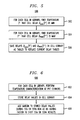
- FIG. 4 illustrates an exemplary method 400 for improving the accuracy of circuit timing analysis, in accordance with one embodiment of the invention.
- Method 400 essentially increases the number of temperature points for each process and voltage (PV) corner used in evaluating circuit timing behavior, and timing sign-off is then performed at each of the PVT corners.
- a set of one or more additional temperatures, T_add, between prescribed minimum and maximum temperatures, T min and T max , respectively, are selected.
- Cell timing characterization for each PVT corner is performed in step 404 at the temperatures in set ⁇ T_add ⁇ generated in step 402 , as well as at the minimum and maximum temperatures T min and T max .
- step 406 timing sign-off is performed for each PVT corner using temperatures from set ⁇ T add ⁇ .
- FIG. 5 illustrates an exemplary method 500 for improving the accuracy of circuit timing analysis, in accordance with another embodiment of the invention.
- Method 500 involves modifying the STA tools and enhancing cell library creation, making cell library delay characterization more conservative in handling temperature used for a given cell or cells. More particularly, rather than using the temperature of the current PVT corner as the temperature of the cell, the delay characterization preferably employs a temperature that produces maximum cell delay for setup-time analysis, and/or a temperature that produces minimum cell delay for hold-time analysis. To implement this methodology, an additional temperature characterization is performed for each cell.
- a first temperature, T′ is determined at which cell delay is minimum.
- a second temperature, T′′ is determined at which cell delay is maximum.
- the minimum cell delay, D min (T) and the maximum cell delay, D max (T′′) are then saved in the cell library in step 506 .
- the minimum and maximum cell delays D min (T′) and D max (T′′) are preferably stored as tables, replacing the current delay tables associated with the cell that were generated using one fixed temperature T corresponding to the library PVT corner.
- the delay calculator will preferably use these new delay tables in the same manner as the previous delay tables which they replaced.
- Method 500 includes advantages that it can employ a traditional timing sign-off methodology, that it may use less temperature corners compared to traditional approaches, and that it is inherently never optimistic, since worst-case delay is actually determined and used. Consequently, there is no risk that some worst-case temperature will be missed.
- method 500 requires an additional cell characterization, requires modification (enhancement) of the delay calculator (it should use minimum or maximum delay table as needed), and is conservative in average timing analysis.
- FIG. 6 illustrates an exemplary method 600 for improving the accuracy of circuit timing analysis, in accordance with another embodiment of the invention.
- Method 600 effectively adds a margin to the output of an STA tool so as to modify the STA results to take into account the effects of temperature on cell timing.
- temperature characterization is first performed for each cell in the library using traditional circuit simulation tools (e.g., HSPICE) and PVT corners.
- the delay values obtained from the characterization are then stored (e.g., in memory) in the cell library in step 604 .
- An additional margin is then added to the stored delay values in step 606 during STA or statistical STA (SSTA) run time, for example, as a de-rating factor, to shift the STA or SSTA results.
- This margin which takes into account temperature variation across the chip, and may incorporate other sources of OCV as well, preferably corrects possible errors in cell delay calculation due to a difference between timing sign-off temperature and real temperature, which may produce worse cell delay.
- method 600 may include, for example, the ability to employ traditional sign-off techniques and tools, simplicity, operation at traditional temperature corners, and controlled risk of device failure.
- method 600 requires the estimation of additional OCV margins and may result in pessimistic delay estimations in order to provide sufficient guarantees that no timing violations will occur.
- FIG. 7 illustrates another exemplary method 700 for improving the accuracy of circuit timing analysis, in accordance with an embodiment of the invention.
- Method 700 which comprises determining all critical paths in a given circuit and then performing a sweeping temperature analysis for these critical paths, provides a significant improvement in the accuracy of the timing analysis and is preferred when the number of timing critical paths is relatively small (e.g., on the order of thousands).
- a critical path which may be identified using standard STA tools, PVT corners, and sign-off methodologies that will report all paths with small timing slack, can be defined as a path having a corresponding timing slack that is less than a prescribed threshold, such as, for example, about 100 ps (the greater the threshold value, the higher the safety margin but the higher the number of reported critical paths).
- step 702 all timing critical paths in the circuit are determined.
- a critical path As many conventional techniques for determining timing critical paths in a circuit. For example, one way to identify the critical path(s) is simply to define a critical path as any signal path in a given design having a timing slack less than some prescribed threshold value, and then to find all such paths using an STA tool or alternative timing analysis methodology.
- these critical paths are usually the longest paths in the design (e.g., paths having a length greater than a prescribed threshold length). This is typically performed post-layout, since the respective lengths of all conductors in the circuit are readily available as an output of the IC layout tool (e.g., Graphic Data System (GDS) II stream format, etc.).
- GDS Graphic Data System
- Circuit simulation is then performed in step 706 on all critical paths using the simulation commands generated in step 704 .
- a circuit simulation program such as, for example, HSPICE or PSpice, can be used to obtain timing characterization data, particularly, path delays, corresponding to the critical paths.
- a Quartus® (a registered trademark of Altera Corporation) II TimeQuest timing analyzer may be used to perform the timing analysis of a given design.
- the Quartus II TimeQuest timing analyzer is operative to analyze the timing paths in the design, calculate the propagation delay along each path, check for timing constraint violations, and report timing results. It is to be understood that the invention is not limited to use with any specific circuit simulation program and/or techniques for predicting path delays in the design.
- Simulation of the critical paths preferably comprises sweeping the temperature within a prescribed range (e.g., ⁇ 20° C.) of each PVT corner temperature.
- a prescribed range e.g., ⁇ 20° C.
- the path delay and/or alternative timing information relating to the critical paths, as reported by the simulation program, is used to determine timing slack (e.g., margins).
- Advantages of method 700 may include, for example, the ability to employ traditional sign-off techniques and tools, accuracy, and the requirement of only a small run-time overhead, assuming the number of critical paths is relatively small.
- this overhead can become significant when the number of critical paths to be evaluated by method 700 is large (e.g., more than about 10,000 paths, which is possible in the case of hold-time analysis).
- FIG. 8 illustrates an exemplary method 800 for improving the accuracy of circuit timing analysis, in accordance with another embodiment of the invention.
- Method 800 which adds a cell delay calculation capability that is temperature dependent for each particular instance of a given cell, provides a significant improvement in the accuracy of the timing analysis and is preferred when the number of timing critical paths is relatively large since this methodology requires significantly less run-time overhead compared to alternative techniques described herein.
- Method 800 is operative to perform cell library characterization for multiple prescribed temperatures in step 802 .
- a traditional delay characterization may be performed not only for prescribed minimum and maximum temperatures, but for several intermediate temperatures, for example, in intervals of 20° C. (e.g., ⁇ 40° C., ⁇ 20° C., 0° C., 20° C., . . . , 120° C.). Each of these temperatures will be associated with some PVT libraries.
- a temperature map is generated corresponding to a physical layout for the design. This may be accomplished, for example, by estimating the temperature for each point on the chip and then generating a temperature gradient map for the chip.
- the temperature map generated in step 804 is then read into a delay calculator in step 806 .
- the delay calculator will have access to the temperature map and should receive, as input data, the specific temperature T(x,y) for each cell that is located in position (x,y).
- the delay calculator preferably determines cell delay at position (x,y) using temperature T(x,y) from the temperature map. This may be accomplished, in one embodiment, by determining which two characterized temperatures, T 1 and T 2 , from the library of PVT corners, the temperature T(x,y) falls between. Then, cell delay corresponding to T(x,y) may be calculated by interpolating between a first delay, D 1 , corresponding to the first PVT corner temperature T 1 from the cell library, and a second delay, D 2 , corresponding to the second PVT corner temperature T 2 (also known as delay scaling). The interpolation may be done, for example, by scaling the delays D 1 and D 2 from the two corresponding PVT libraries. The cell delay calculation may then be incorporated into a timing report for the cell by modifying at least one parameter of the timing characterization for the cell, although alternative techniques for incorporating the cell delay calculation results into the timing report are similarly contemplated.
- Advantages of method 800 include, for example, the ability to employ traditional sign-off techniques and tools, the use of traditional temperature corners in the cell library, high accuracy, and the requirement of only a small run-time overhead.
- a trade-off for these advantages includes the requirement of additional PVT corners characterization, modification to the delay calculator, and the need to calculate a temperature map for the given cell layout.
- one or more parameters of the circuit are preferably analyzed and/or modified so as to optimize a performance and/or reliability of the circuit, at least in terms of reducing a sensitivity of the circuit to the effects of temperature inversion. More particularly, results of the static timing analysis performed on the circuit may be used to determine whether or not the circuit will operate within prescribed parameters corresponding to the circuit. Benefits of the present invention include the ability to more accurately predict circuit performance over variations in temperature, thereby saving time and cost in a design process of the circuit.
- processor 910 a processor 910
- memory 920 a memory 920
- I/O interface 930 which may include, for example, a display and a keyboard (not explicitly shown).
- processor as used herein is intended to include any processing device, such as, for example, one that includes a CPU (central processing unit) and/or other forms of processing circuitry. Further, the term “processor” may refer to more than one individual processor.
- memory is intended to include memory associated with a processor or CPU, such as, for example, RAM (random access memory), ROM (read only memory), a fixed memory device (for example, hard drive), a removable memory device (for example, diskette), a flash memory and the like.
- input/output interface is intended to include, for example, one or more mechanisms for inputting data to the processing unit (for example, mouse), and one or more mechanisms for providing results associated with the processing unit (for example, printer).
- the processor 910 , memory 920 , and I/O interface 930 can be interconnected, for example, via bus 940 as part of a data processing unit 900 .
- Suitable interconnections can also be provided to a network interface (not explicitly shown), such as a network card, which can be provided to interface with a computer network, and to a media interface, such as a diskette or CD-ROM drive, which can be provided to interface with media.
- a network interface such as a network card, which can be provided to interface with a computer network
- a media interface such as a diskette or CD-ROM drive
- computer software including instructions or code for performing the methodologies of the invention, as described herein, may be stored in one or more of the associated memory devices (for example, ROM, fixed or removable memory) and, when ready to be utilized, loaded in part or in whole (for example, into RAM) and executed by a CPU.
- Such software could include, but is not limited to, firmware, resident software, microcode, and the like.
- the invention can take the form of a computer program product accessible from a computer-usable or computer-readable medium providing program code for use by or in connection with a computer or any instruction execution system.
- a computer usable or computer readable medium can be any apparatus for use by or in connection with the instruction execution system, apparatus, or device.
- the medium can be an electronic, magnetic, optical, electromagnetic, infrared, or semiconductor system (or apparatus or device) or a propagation medium.
- Examples of a computer-readable medium include a semiconductor or solid-state memory (for example memory 920 ), magnetic tape, a removable computer diskette, a random access memory (RAM), a read-only memory (ROM), a rigid magnetic disk and an optical disk.
- Current examples of optical disks include compact disk-read only memory (CD-ROM), compact disk-read/write (CD-R/W) and DVD.
- An electronic system preferably a data processing system, suitable for storing and/or executing program code will include at least one processor 910 coupled directly or indirectly to memory elements 920 through system bus 940 .
- the memory elements can include local memory employed during actual execution of the program code, bulk storage, and cache memories which provide temporary storage of at least some program code in order to reduce the number of times code must be retrieved from bulk storage during execution.
- Network adapters such as network interface (not explicitly shown) may also be coupled to the system to enable the data processing system to become coupled to other data processing systems or remote printers or storage devices through intervening private or public networks.
- Modems, cable modem and Ethernet cards are just a few of the currently available types of network adapters.
- At least a portion of the circuits and methodologies of the present invention may be implemented in one or more integrated circuits.
- die are typically fabricated in a repeated pattern on a surface of a semiconductor wafer.
- Each of the die includes a device described herein, and may include other structures or circuits.
- Individual die are cut or diced from the wafer, then packaged as integrated circuits.
- One skilled in the art would know how to dice wafers and package die to produce integrated circuits. Integrated circuits so manufactured are considered part of this invention.
- An integrated circuit in accordance with the present invention can be employed in any application and/or electronic system which utilizes memory, embedded or otherwise.
- Suitable systems for implementing techniques of the invention may include, but are not limited to, personal computers, communication networks, electronic instruments (e.g., automated test equipment (ATE)), interface networks, etc. Systems incorporating such integrated circuits are considered part of this invention. Given the teachings of the invention provided herein, one of ordinary skill in the art will be able to contemplate other implementations and applications of the techniques of the invention.
Landscapes
- Engineering & Computer Science (AREA)
- Computer Hardware Design (AREA)
- Physics & Mathematics (AREA)
- Theoretical Computer Science (AREA)
- Evolutionary Computation (AREA)
- Geometry (AREA)
- General Engineering & Computer Science (AREA)
- General Physics & Mathematics (AREA)
- Design And Manufacture Of Integrated Circuits (AREA)
Abstract
Description
D(C,T)=a(C)T+b(C),
where a and b are constants for cell C. Note that a<0 for cells exhibiting temperature inversion, at least for one or more ramp-time and/or load combinations.
Thus, each signal path P in the circuit may experience temperature inversion (e.g., A<0) or may not experience temperature inversion (e.g., A>0) depending on the combination(s) of cells in the path and their respective ramp-times and/or loads.
Claims (8)
Priority Applications (2)
| Application Number | Priority Date | Filing Date | Title |
|---|---|---|---|
| US13/453,289 US8645888B2 (en) | 2008-10-14 | 2012-04-23 | Circuit timing analysis incorporating the effects of temperature inversion |
| US14/093,189 US20140089881A1 (en) | 2008-10-14 | 2013-11-29 | Circuit Timing Analysis Incorporating the Effects of Temperature Inversion |
Applications Claiming Priority (2)
| Application Number | Priority Date | Filing Date | Title |
|---|---|---|---|
| US12/251,088 US8181144B2 (en) | 2008-10-14 | 2008-10-14 | Circuit timing analysis incorporating the effects of temperature inversion |
| US13/453,289 US8645888B2 (en) | 2008-10-14 | 2012-04-23 | Circuit timing analysis incorporating the effects of temperature inversion |
Related Parent Applications (1)
| Application Number | Title | Priority Date | Filing Date |
|---|---|---|---|
| US12/251,088 Division US8181144B2 (en) | 2008-10-14 | 2008-10-14 | Circuit timing analysis incorporating the effects of temperature inversion |
Related Child Applications (1)
| Application Number | Title | Priority Date | Filing Date |
|---|---|---|---|
| US14/093,189 Division US20140089881A1 (en) | 2008-10-14 | 2013-11-29 | Circuit Timing Analysis Incorporating the Effects of Temperature Inversion |
Publications (2)
| Publication Number | Publication Date |
|---|---|
| US20120210287A1 US20120210287A1 (en) | 2012-08-16 |
| US8645888B2 true US8645888B2 (en) | 2014-02-04 |
Family
ID=42100040
Family Applications (3)
| Application Number | Title | Priority Date | Filing Date |
|---|---|---|---|
| US12/251,088 Active 2030-09-30 US8181144B2 (en) | 2008-10-14 | 2008-10-14 | Circuit timing analysis incorporating the effects of temperature inversion |
| US13/453,289 Active US8645888B2 (en) | 2008-10-14 | 2012-04-23 | Circuit timing analysis incorporating the effects of temperature inversion |
| US14/093,189 Abandoned US20140089881A1 (en) | 2008-10-14 | 2013-11-29 | Circuit Timing Analysis Incorporating the Effects of Temperature Inversion |
Family Applications Before (1)
| Application Number | Title | Priority Date | Filing Date |
|---|---|---|---|
| US12/251,088 Active 2030-09-30 US8181144B2 (en) | 2008-10-14 | 2008-10-14 | Circuit timing analysis incorporating the effects of temperature inversion |
Family Applications After (1)
| Application Number | Title | Priority Date | Filing Date |
|---|---|---|---|
| US14/093,189 Abandoned US20140089881A1 (en) | 2008-10-14 | 2013-11-29 | Circuit Timing Analysis Incorporating the Effects of Temperature Inversion |
Country Status (1)
| Country | Link |
|---|---|
| US (3) | US8181144B2 (en) |
Cited By (4)
| Publication number | Priority date | Publication date | Assignee | Title |
|---|---|---|---|---|
| US20140089881A1 (en) * | 2008-10-14 | 2014-03-27 | Lsi Corporation | Circuit Timing Analysis Incorporating the Effects of Temperature Inversion |
| WO2014165077A2 (en) | 2013-03-12 | 2014-10-09 | Saudi Arabian Oil Company | Oil field process control system |
| US10360334B2 (en) | 2017-02-09 | 2019-07-23 | Globalfoundries Inc. | Context aware processing to resolve strong spacing effects due to strain relaxation in standard cell library |
| US10365698B2 (en) | 2017-07-27 | 2019-07-30 | Oracle International Corporation | Temperature based frequency throttling |
Families Citing this family (27)
| Publication number | Priority date | Publication date | Assignee | Title |
|---|---|---|---|---|
| US8499230B2 (en) * | 2008-05-07 | 2013-07-30 | Lsi Corporation | Critical path monitor for an integrated circuit and method of operation thereof |
| US8239805B2 (en) | 2009-07-27 | 2012-08-07 | Lsi Corporation | Method for designing integrated circuits employing a partitioned hierarchical design flow and an apparatus employing the method |
| US9672315B2 (en) * | 2009-08-05 | 2017-06-06 | Taiwan Semiconductor Manufacturing Company, Ltd. | Optimization for circuit migration |
| JP2011113302A (en) * | 2009-11-26 | 2011-06-09 | Renesas Electronics Corp | Timing verification device for semiconductor integrated circuit, timing verification method, and timing verification program |
| JP2011114328A (en) * | 2009-11-30 | 2011-06-09 | Toshiba Corp | Method and device for constructing spice corner model |
| US8336010B1 (en) * | 2009-12-04 | 2012-12-18 | Cadence Design Systems, Inc. | Design-specific on chip variation de-rating factors for static timing analysis of integrated circuits |
| US9047426B2 (en) * | 2010-06-07 | 2015-06-02 | Riverbed Technology, Inc. | Performing scenario reduction in a circuit design flow |
| US8499274B2 (en) * | 2011-11-30 | 2013-07-30 | Taiwan Semiconductor Manufacturing Co., Ltd. | Computer implemented system and method for leakage calculation |
| US20130253868A1 (en) * | 2012-03-23 | 2013-09-26 | International Business Machines Corporation | Estimating delay deterioration due to device degradation in integrated circuits |
| US8543960B1 (en) | 2012-05-31 | 2013-09-24 | International Business Machines Corporation | Power and timing optimization for an integrated circuit by voltage modification across various ranges of temperatures |
| US8839170B2 (en) | 2012-05-31 | 2014-09-16 | International Business Machines Corporation | Power/performance optimization through temperature/voltage control |
| US9141742B2 (en) * | 2012-12-31 | 2015-09-22 | Synopsys, Inc. | Priori corner and mode reduction |
| US8839165B2 (en) | 2013-01-25 | 2014-09-16 | International Business Machines Corporation | Power/performance optimization through continuously variable temperature-based voltage control |
| US9264027B1 (en) * | 2013-03-14 | 2016-02-16 | Integrated Device Technology, Inc. | Process compensated delay |
| JP2015135650A (en) * | 2014-01-20 | 2015-07-27 | 富士通セミコンダクター株式会社 | Design method, design device and program |
| US9594858B1 (en) * | 2014-09-23 | 2017-03-14 | Cadence Design Systems, Inc. | Methods, systems, and articles of manufacture for implementing scalable statistical library characterization for electronic designs |
| US9519747B1 (en) * | 2015-06-26 | 2016-12-13 | Globalfoundries Inc. | Dynamic and adaptive timing sensitivity during static timing analysis using look-up table |
| US10169523B2 (en) * | 2015-08-27 | 2019-01-01 | International Business Machines Corporation | Timing constraints formulation for highly replicated design modules |
| US9934341B2 (en) * | 2015-11-11 | 2018-04-03 | International Business Machines Corporation | Simulation of modifications to microprocessor design |
| US9501609B1 (en) | 2015-12-02 | 2016-11-22 | International Business Machines Corporation | Selection of corners and/or margins using statistical static timing analysis of an integrated circuit |
| US9859889B2 (en) | 2016-02-03 | 2018-01-02 | Electronics And Telecommunications Research Institute | Ultra low voltage digital circuit and operation method thereof |
| US10037394B1 (en) | 2016-06-14 | 2018-07-31 | Cadence Design Systems, Inc. | Hierarchical timing analysis for multi-instance blocks |
| US10169501B1 (en) * | 2016-06-14 | 2019-01-01 | Cadence Design Systems, Inc. | Timing context generation with multi-instance blocks for hierarchical analysis |
| US10340903B2 (en) | 2016-11-24 | 2019-07-02 | Electronics & Telecommunications Research Institute | Semiconductor device and operation method thereof |
| KR102603299B1 (en) * | 2017-12-08 | 2023-11-17 | 한국전자통신연구원 | Graphics processing unit and operating method of the same |
| CN112257953B (en) * | 2020-11-03 | 2021-09-24 | 上海电力大学 | Data processing method based on polar region new energy power generation power prediction |
| CN114021514B (en) * | 2021-11-26 | 2024-07-05 | 北京华大九天科技股份有限公司 | Method for simulating and screening bottleneck units through SPICE voltage or temperature scanning |
Citations (21)
| Publication number | Priority date | Publication date | Assignee | Title |
|---|---|---|---|---|
| US5802349A (en) * | 1996-01-22 | 1998-09-01 | Motorola, Inc. | Method for generating an optimized integrated circuit cell library |
| US6090152A (en) * | 1997-03-20 | 2000-07-18 | International Business Machines Corporation | Method and system for using voltage and temperature adders to account for variations in operating conditions during timing simulation |
| US20020174409A1 (en) * | 2001-05-21 | 2002-11-21 | International Business Machines Corporation | System and method for analyzing power distribution using static timing analysis |
| US20030102511A1 (en) * | 2001-11-08 | 2003-06-05 | Hiroyuki Kuge | CMOS buffer circuit |
| US6609238B1 (en) | 2001-06-15 | 2003-08-19 | Lsi Logic Corporation | Method of control cell placement to minimize connection length and cell delay |
| US20040025136A1 (en) | 2002-07-30 | 2004-02-05 | Carelli John A. | Method for designing a custom ASIC library |
| US7092838B1 (en) * | 2004-06-04 | 2006-08-15 | Sierra Design Automation, Inc. | Method and apparatus for the analysis and optimization of variability in nanometer technologies |
| US20070006106A1 (en) | 2005-06-30 | 2007-01-04 | Texas Instruments Incorporated | Method and system for desensitization of chip designs from perturbations affecting timing and manufacturability |
| US20070050092A1 (en) | 2005-08-12 | 2007-03-01 | Symyx Technologies, Inc. | Event-based library process design |
| US20070226660A1 (en) * | 2006-03-24 | 2007-09-27 | Fujitsu Limited | Designing and operating of semiconductor integrated circuit by taking into account process variation |
| US20070234254A1 (en) * | 2006-03-31 | 2007-10-04 | Fujitsu Limited | Timing analyzing method and apparatus for semiconductor integrated circuit |
| US7391272B2 (en) * | 2005-11-23 | 2008-06-24 | Oki Electric Industry Co., Ltd. | Voltage controlled oscillator with full adder |
| US7500206B2 (en) * | 2004-02-26 | 2009-03-03 | Nec Electronics Corporation | Delay time verifying method with less processing load |
| US20090077514A1 (en) * | 2007-09-13 | 2009-03-19 | Behnam Malek-Khosravi | Area and power saving standard cell methodology |
| US20090217226A1 (en) * | 2008-02-26 | 2009-08-27 | Qian Cui | Multiple derating factor sets for delay calculation and library generation in multi-corner STA sign-off flow |
| US7669154B2 (en) * | 2005-03-29 | 2010-02-23 | Fujitsu Microelectronics Limited | Timing analysis method, timing analysis program, and timing analysis tool |
| US20100095260A1 (en) * | 2008-10-14 | 2010-04-15 | Alexander Tetelbaum | Reducing Path Delay Sensitivity to Temperature Variation in Timing-Critical Paths |
| US7795939B2 (en) * | 2008-12-29 | 2010-09-14 | Taiwan Semiconductor Manufacturing Company, Ltd. | Method and system for setup/hold characterization in sequential cells |
| US7882471B1 (en) * | 2005-11-15 | 2011-02-01 | Cadence Design Systems, Inc. | Timing and signal integrity analysis of integrated circuits with semiconductor process variations |
| US20110126163A1 (en) * | 2009-11-24 | 2011-05-26 | International Business Machines Corporation | Method to reduce delay variation by sensitivity cancellation |
| US20110138347A1 (en) * | 2008-08-14 | 2011-06-09 | Icera Inc. | System and method for designing integrated circuits that employ adaptive voltage scaling optimization |
Family Cites Families (10)
| Publication number | Priority date | Publication date | Assignee | Title |
|---|---|---|---|---|
| US6480991B1 (en) * | 2001-04-11 | 2002-11-12 | International Business Machines Corporation | Timing-driven global placement based on geometry-aware timing budgets |
| US7107558B2 (en) * | 2003-06-09 | 2006-09-12 | Lsi Logic Corporation | Method of finding critical nets in an integrated circuit design |
| US7424693B2 (en) * | 2005-10-20 | 2008-09-09 | Agere Systems Inc. | Methods for measurement and prediction of hold-time and exceeding hold time limits due to cells with tied input pins |
| US7475366B2 (en) * | 2006-08-04 | 2009-01-06 | International Business Machines Corporation | Integrated circuit design closure method for selective voltage binning |
| US8726289B2 (en) * | 2008-02-22 | 2014-05-13 | International Business Machines Corporation | Streaming attachment of hardware accelerators to computer systems |
| US8499230B2 (en) * | 2008-05-07 | 2013-07-30 | Lsi Corporation | Critical path monitor for an integrated circuit and method of operation thereof |
| US20100050144A1 (en) * | 2008-08-25 | 2010-02-25 | Lsi Corporation | System and method for employing signoff-quality timing analysis information to reduce leakage power in an electronic circuit and electronic design automation tool incorporating the same |
| US8112734B2 (en) * | 2008-09-29 | 2012-02-07 | Lsi Corporation | Optimization with adaptive body biasing |
| US8181144B2 (en) * | 2008-10-14 | 2012-05-15 | Lsi Corporation | Circuit timing analysis incorporating the effects of temperature inversion |
| US8560990B2 (en) * | 2010-01-13 | 2013-10-15 | International Business Machines Corporation | Method of managing electro migration in logic designs and design structure thereof |
-
2008
- 2008-10-14 US US12/251,088 patent/US8181144B2/en active Active
-
2012
- 2012-04-23 US US13/453,289 patent/US8645888B2/en active Active
-
2013
- 2013-11-29 US US14/093,189 patent/US20140089881A1/en not_active Abandoned
Patent Citations (24)
| Publication number | Priority date | Publication date | Assignee | Title |
|---|---|---|---|---|
| US5802349A (en) * | 1996-01-22 | 1998-09-01 | Motorola, Inc. | Method for generating an optimized integrated circuit cell library |
| US6090152A (en) * | 1997-03-20 | 2000-07-18 | International Business Machines Corporation | Method and system for using voltage and temperature adders to account for variations in operating conditions during timing simulation |
| US20020174409A1 (en) * | 2001-05-21 | 2002-11-21 | International Business Machines Corporation | System and method for analyzing power distribution using static timing analysis |
| US6609238B1 (en) | 2001-06-15 | 2003-08-19 | Lsi Logic Corporation | Method of control cell placement to minimize connection length and cell delay |
| US20030102511A1 (en) * | 2001-11-08 | 2003-06-05 | Hiroyuki Kuge | CMOS buffer circuit |
| US20040025136A1 (en) | 2002-07-30 | 2004-02-05 | Carelli John A. | Method for designing a custom ASIC library |
| US7500206B2 (en) * | 2004-02-26 | 2009-03-03 | Nec Electronics Corporation | Delay time verifying method with less processing load |
| US7092838B1 (en) * | 2004-06-04 | 2006-08-15 | Sierra Design Automation, Inc. | Method and apparatus for the analysis and optimization of variability in nanometer technologies |
| US7669154B2 (en) * | 2005-03-29 | 2010-02-23 | Fujitsu Microelectronics Limited | Timing analysis method, timing analysis program, and timing analysis tool |
| US20070006106A1 (en) | 2005-06-30 | 2007-01-04 | Texas Instruments Incorporated | Method and system for desensitization of chip designs from perturbations affecting timing and manufacturability |
| US20070050092A1 (en) | 2005-08-12 | 2007-03-01 | Symyx Technologies, Inc. | Event-based library process design |
| US7882471B1 (en) * | 2005-11-15 | 2011-02-01 | Cadence Design Systems, Inc. | Timing and signal integrity analysis of integrated circuits with semiconductor process variations |
| US7391272B2 (en) * | 2005-11-23 | 2008-06-24 | Oki Electric Industry Co., Ltd. | Voltage controlled oscillator with full adder |
| US20070226660A1 (en) * | 2006-03-24 | 2007-09-27 | Fujitsu Limited | Designing and operating of semiconductor integrated circuit by taking into account process variation |
| US7661079B2 (en) * | 2006-03-24 | 2010-02-09 | Fujitsu Microelectronics Limited | Designing and operating of semiconductor integrated circuit by taking into account process variation |
| US7464355B2 (en) * | 2006-03-31 | 2008-12-09 | Fujitsu Limited | Timing analyzing method and apparatus for semiconductor integrated circuit |
| US20070234254A1 (en) * | 2006-03-31 | 2007-10-04 | Fujitsu Limited | Timing analyzing method and apparatus for semiconductor integrated circuit |
| US20090077514A1 (en) * | 2007-09-13 | 2009-03-19 | Behnam Malek-Khosravi | Area and power saving standard cell methodology |
| US20100188060A1 (en) * | 2007-09-13 | 2010-07-29 | Behnam Malek-Khosravi | Area and power saving standard cell methodology |
| US20090217226A1 (en) * | 2008-02-26 | 2009-08-27 | Qian Cui | Multiple derating factor sets for delay calculation and library generation in multi-corner STA sign-off flow |
| US20110138347A1 (en) * | 2008-08-14 | 2011-06-09 | Icera Inc. | System and method for designing integrated circuits that employ adaptive voltage scaling optimization |
| US20100095260A1 (en) * | 2008-10-14 | 2010-04-15 | Alexander Tetelbaum | Reducing Path Delay Sensitivity to Temperature Variation in Timing-Critical Paths |
| US7795939B2 (en) * | 2008-12-29 | 2010-09-14 | Taiwan Semiconductor Manufacturing Company, Ltd. | Method and system for setup/hold characterization in sequential cells |
| US20110126163A1 (en) * | 2009-11-24 | 2011-05-26 | International Business Machines Corporation | Method to reduce delay variation by sensitivity cancellation |
Non-Patent Citations (2)
| Title |
|---|
| A. Dasdan et al., "Handling Inverted Temperature Dependence in Static Timing Analysis," ACM Transactions on Design Automation of Electronic Systems, Apr. 2006, pp. 306-324, vol. 11, No. 2. |
| A. Tetelbaum et al., "Impact of Temperature Inversion on Timing Sign-off and Design Methodology," Presented at Microprocessor Test and Verification Workshop, Dec. 2007, pp. 1-7. |
Cited By (9)
| Publication number | Priority date | Publication date | Assignee | Title |
|---|---|---|---|---|
| US20140089881A1 (en) * | 2008-10-14 | 2014-03-27 | Lsi Corporation | Circuit Timing Analysis Incorporating the Effects of Temperature Inversion |
| WO2014165077A2 (en) | 2013-03-12 | 2014-10-09 | Saudi Arabian Oil Company | Oil field process control system |
| EP3147739A1 (en) | 2013-03-12 | 2017-03-29 | Saudi Arabian Oil Company | Oil field process control system |
| US10360334B2 (en) | 2017-02-09 | 2019-07-23 | Globalfoundries Inc. | Context aware processing to resolve strong spacing effects due to strain relaxation in standard cell library |
| US10365698B2 (en) | 2017-07-27 | 2019-07-30 | Oracle International Corporation | Temperature based frequency throttling |
| US10990145B2 (en) | 2017-07-27 | 2021-04-27 | Oracle International Corporation | Temperature based frequency throttling |
| US11550376B2 (en) | 2017-07-27 | 2023-01-10 | Oracle International Corporation | Temperature based frequency throttling |
| US20230161394A1 (en) * | 2017-07-27 | 2023-05-25 | Oracle International Corporation | Temperature based frequency throttling |
| US11899513B2 (en) * | 2017-07-27 | 2024-02-13 | Oracle International Corporation | Temperature based frequency throttling |
Also Published As
| Publication number | Publication date |
|---|---|
| US20120210287A1 (en) | 2012-08-16 |
| US20100095259A1 (en) | 2010-04-15 |
| US8181144B2 (en) | 2012-05-15 |
| US20140089881A1 (en) | 2014-03-27 |
Similar Documents
| Publication | Publication Date | Title |
|---|---|---|
| US8645888B2 (en) | Circuit timing analysis incorporating the effects of temperature inversion | |
| US8336010B1 (en) | Design-specific on chip variation de-rating factors for static timing analysis of integrated circuits | |
| Wirnshofer | Variation-aware adaptive voltage scaling for digital CMOS circuits | |
| US7555740B2 (en) | Method and system for evaluating statistical sensitivity credit in path-based hybrid multi-corner static timing analysis | |
| US8255850B2 (en) | Fabricating IC with NBTI path delay within timing constraints | |
| Kahng | New game, new goal posts: A recent history of timing closure | |
| US20120123745A1 (en) | Adaptive Content-aware Aging Simulations | |
| JP2005092885A (en) | System and method for statistical timing analysis of digital circuits | |
| US8056035B2 (en) | Method and system for analyzing cross-talk coupling noise events in block-based statistical static timing | |
| US10789406B1 (en) | Characterizing electronic component parameters including on-chip variations and moments | |
| US20100153897A1 (en) | System and method for employing signoff-quality timing analysis information concurrently in multiple scenarios to reduce leakage power in an electronic circuit and electronic design automation tool incorporating the same | |
| US8225257B2 (en) | Reducing path delay sensitivity to temperature variation in timing-critical paths | |
| Velamala et al. | Failure diagnosis of asymmetric aging under NBTI | |
| Zhang et al. | Aging-aware gate-level modeling for circuit reliability analysis | |
| Chan et al. | Impact of adaptive voltage scaling on aging-aware signoff | |
| Golanbari et al. | Aging guardband reduction through selective flip-flop optimization | |
| US20140040845A1 (en) | System and method for employing side transition times from signoff-quality timing analysis information to reduce leakage power in an electronic circuit and an electronic design automation tool incorporating the same | |
| US7885798B2 (en) | Closed-loop modeling of gate leakage for fast simulators | |
| US20170193151A1 (en) | Adaptive characterization and instantiation of timing abstracts | |
| Freijedo et al. | Modeling the effect of process, power-supply voltage and temperature variations on the timing response of nanometer digital circuits | |
| Duan et al. | An ageing-aware digital synthesis approach | |
| US10372851B2 (en) | Independently projecting a canonical clock | |
| Gomez et al. | An efficient metric-guided gate sizing methodology for guardband reduction under process variations and aging effects | |
| Rita et al. | Timing analysis journey from OCV to LVF | |
| Nesset | Rtl power estimation flow and its use in power optimization |
Legal Events
| Date | Code | Title | Description |
|---|---|---|---|
| STCF | Information on status: patent grant |
Free format text: PATENTED CASE |
|
| AS | Assignment |
Owner name: DEUTSCHE BANK AG NEW YORK BRANCH, AS COLLATERAL AG Free format text: PATENT SECURITY AGREEMENT;ASSIGNORS:LSI CORPORATION;AGERE SYSTEMS LLC;REEL/FRAME:032856/0031 Effective date: 20140506 |
|
| AS | Assignment |
Owner name: AVAGO TECHNOLOGIES GENERAL IP (SINGAPORE) PTE. LTD Free format text: ASSIGNMENT OF ASSIGNORS INTEREST;ASSIGNOR:LSI CORPORATION;REEL/FRAME:035390/0388 Effective date: 20140814 |
|
| AS | Assignment |
Owner name: LSI CORPORATION, CALIFORNIA Free format text: TERMINATION AND RELEASE OF SECURITY INTEREST IN PATENT RIGHTS (RELEASES RF 032856-0031);ASSIGNOR:DEUTSCHE BANK AG NEW YORK BRANCH, AS COLLATERAL AGENT;REEL/FRAME:037684/0039 Effective date: 20160201 Owner name: AGERE SYSTEMS LLC, PENNSYLVANIA Free format text: TERMINATION AND RELEASE OF SECURITY INTEREST IN PATENT RIGHTS (RELEASES RF 032856-0031);ASSIGNOR:DEUTSCHE BANK AG NEW YORK BRANCH, AS COLLATERAL AGENT;REEL/FRAME:037684/0039 Effective date: 20160201 |
|
| AS | Assignment |
Owner name: BANK OF AMERICA, N.A., AS COLLATERAL AGENT, NORTH CAROLINA Free format text: PATENT SECURITY AGREEMENT;ASSIGNOR:AVAGO TECHNOLOGIES GENERAL IP (SINGAPORE) PTE. LTD.;REEL/FRAME:037808/0001 Effective date: 20160201 Owner name: BANK OF AMERICA, N.A., AS COLLATERAL AGENT, NORTH Free format text: PATENT SECURITY AGREEMENT;ASSIGNOR:AVAGO TECHNOLOGIES GENERAL IP (SINGAPORE) PTE. LTD.;REEL/FRAME:037808/0001 Effective date: 20160201 |
|
| AS | Assignment |
Owner name: AVAGO TECHNOLOGIES GENERAL IP (SINGAPORE) PTE. LTD., SINGAPORE Free format text: TERMINATION AND RELEASE OF SECURITY INTEREST IN PATENTS;ASSIGNOR:BANK OF AMERICA, N.A., AS COLLATERAL AGENT;REEL/FRAME:041710/0001 Effective date: 20170119 Owner name: AVAGO TECHNOLOGIES GENERAL IP (SINGAPORE) PTE. LTD Free format text: TERMINATION AND RELEASE OF SECURITY INTEREST IN PATENTS;ASSIGNOR:BANK OF AMERICA, N.A., AS COLLATERAL AGENT;REEL/FRAME:041710/0001 Effective date: 20170119 |
|
| FEPP | Fee payment procedure |
Free format text: MAINTENANCE FEE REMINDER MAILED (ORIGINAL EVENT CODE: REM.) |
|
| AS | Assignment |
Owner name: BELL SEMICONDUCTOR, LLC, ILLINOIS Free format text: ASSIGNMENT OF ASSIGNORS INTEREST;ASSIGNORS:AVAGO TECHNOLOGIES GENERAL IP (SINGAPORE) PTE. LTD.;BROADCOM CORPORATION;REEL/FRAME:044887/0109 Effective date: 20171208 |
|
| FEPP | Fee payment procedure |
Free format text: SURCHARGE FOR LATE PAYMENT, LARGE ENTITY (ORIGINAL EVENT CODE: M1554) |
|
| MAFP | Maintenance fee payment |
Free format text: PAYMENT OF MAINTENANCE FEE, 4TH YEAR, LARGE ENTITY (ORIGINAL EVENT CODE: M1551) Year of fee payment: 4 |
|
| AS | Assignment |
Owner name: CORTLAND CAPITAL MARKET SERVICES LLC, AS COLLATERA Free format text: SECURITY INTEREST;ASSIGNORS:HILCO PATENT ACQUISITION 56, LLC;BELL SEMICONDUCTOR, LLC;BELL NORTHERN RESEARCH, LLC;REEL/FRAME:045216/0020 Effective date: 20180124 |
|
| MAFP | Maintenance fee payment |
Free format text: PAYMENT OF MAINTENANCE FEE, 8TH YEAR, LARGE ENTITY (ORIGINAL EVENT CODE: M1552); ENTITY STATUS OF PATENT OWNER: LARGE ENTITY Year of fee payment: 8 |
|
| AS | Assignment |
Owner name: BELL NORTHERN RESEARCH, LLC, ILLINOIS Free format text: RELEASE BY SECURED PARTY;ASSIGNOR:CORTLAND CAPITAL MARKET SERVICES LLC;REEL/FRAME:059720/0223 Effective date: 20220401 Owner name: BELL SEMICONDUCTOR, LLC, ILLINOIS Free format text: RELEASE BY SECURED PARTY;ASSIGNOR:CORTLAND CAPITAL MARKET SERVICES LLC;REEL/FRAME:059720/0223 Effective date: 20220401 Owner name: HILCO PATENT ACQUISITION 56, LLC, ILLINOIS Free format text: RELEASE BY SECURED PARTY;ASSIGNOR:CORTLAND CAPITAL MARKET SERVICES LLC;REEL/FRAME:059720/0223 Effective date: 20220401 |