US8643159B2 - Lead frame with grooved lead finger - Google Patents
Lead frame with grooved lead finger Download PDFInfo
- Publication number
- US8643159B2 US8643159B2 US13/441,924 US201213441924A US8643159B2 US 8643159 B2 US8643159 B2 US 8643159B2 US 201213441924 A US201213441924 A US 201213441924A US 8643159 B2 US8643159 B2 US 8643159B2
- Authority
- US
- United States
- Prior art keywords
- channels
- bond
- substrate
- lead
- lead frame
- Prior art date
- Legal status (The legal status is an assumption and is not a legal conclusion. Google has not performed a legal analysis and makes no representation as to the accuracy of the status listed.)
- Active
Links
Images


Classifications
-
- H10W72/072—
-
- H10W70/424—
-
- H10W70/042—
-
- H10W70/048—
-
- H10W70/465—
-
- H10W72/07141—
-
- H10W72/073—
-
- H10W72/075—
-
- H10W72/07521—
-
- H10W72/07533—
-
- H10W72/5363—
-
- H10W72/5522—
-
- H10W72/5524—
-
- H10W72/5525—
-
- H10W72/931—
-
- H10W74/00—
-
- H10W90/754—
-
- H10W90/756—
Definitions
- the present invention relates generally to semiconductor devices, and more particularly to a lead frame having a grooved tip for securing a bond wire to the tip.
- Wire bonding technology is used for connecting bond wires between a semiconductor die and lead fingers of a lead frame or substrate electrical connection pads.
- the wire bonding process includes feeding the bond wire through a capillary of a wire bonding device and using the capillary to facilitate the bonding of the wire to the die and the lead frame or substrate.
- FIG. 1 is a cross-sectional view of a conventional semiconductor device 10 having a semiconductor die 12 , a lead frame 14 having a die flag 16 and lead fingers 18 surrounding the die flag 16 , bond wires 20 extending between the die 12 and the lead fingers 18 , and a molding compound 22 that encapsulates the semiconductor die 12 and bond wires 20 .
- the bond wires 20 are attached and electrically connected to bond pads of the die and ends of the lead fingers (or substrate) with a wire bonding machine by applying ultrasonic pressure and heat.
- a bond wire is threaded through a capillary and then a free end of the bond wire is first melted to form a free air ball (FAB).
- the FAB is attached to the die bond pad by pressing the FAB against a die bond pad and applying thermal and ultrasonic energy.
- the bond wire 20 is then moved to the surface of a respective lead finger 18 of the lead frame 14 using the wire bonding device and then pressed onto the surface of the lead finger 18 again by applying ultrasonic and thermal energy.
- the capillary pulls on and breaks the wire 20 from the lead finger 18 and then the process is repeated with the capillary going from die bond pad to lead finger.
- FIG. 2 is an illustration of the bond wire 20 being attached to a lead finger or the lead frame 14 with a capillary 30 .
- This bond usually is called a stitch bond 32 .
- the bond to the die bond pad sometimes is referred to as the first bond and the bond to the lead finger as the second bond.
- One problem in semiconductor device assembly is a poor second bond. That is, a stitch bond generally is not as reliable as a ball bond. For example, For example, the second bond
- FIGS. 3 , 4 and 5 are photographs of poor or compromised second bonds.
- FIG. 3 is a picture 40 of a broken stitch bond 42 that was damaged when the substrate was subjected to an open/short failure test.
- FIG. 4 is a picture 44 of a broken stitch bond 46 that was damaged in a similar manner.
- FIG. 5 is a picture 48 of two stitch bonds 50 and 52 having heel cracks.
- FIG. 1 is an enlarged cross-sectional, side view of a conventional semiconductor package
- FIG. 2 illustrates the formation of a conventional stitch bond or second bond
- FIG. 3 is a photograph of a broken stitch bond that was formed using a conventional bonding process after being subjected to an open/short failure test;
- FIG. 4 is another photograph of a broken stitch bond that was formed using a conventional bonding process after being subjected to an open/short failure test;
- FIG. 5 is a photograph of a stitch bond formed using a conventional bonding process after being subjected to an open/short failure test
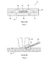
- FIG. 6 is a side cross-sectional view showing a substrate with channels formed on a substrate electrical connection pad of the substrate in accordance with an embodiment of the present invention
- FIG. 7 is a side cross-sectional view of the substrate of FIG. 6 with a bond wire attached thereto;
- FIG. 8 is a side cross-sectional view of a substrate with a bond wire attached thereto in accordance with another embodiment of the present invention.
- FIG. 9 is a top plan view of a substrate electrical connection pad in accordance with an embodiment of the present invention.
- the present invention provides a method of wire bonding.
- a substrate having a plurality of channels formed on a substrate electrical connection pad of the substrate is provided.
- a stitch bond of a wire is formed on the substrate such that a first end of the wire is embedded within the plurality of channels of the substrate.
- the present invention is a semiconductor device.
- the semiconductor device includes a substrate having a plurality of channels formed on a substrate electrical connection pad.
- a semiconductor die is attached to a die-attach area of the substrate and bond wires are electrically coupled to the substrate and to the semiconductor die.
- An end of each bond wire is embedded within the channels of the substrate to form a secure bond on the substrate electrical connection pad.
- the substrate 60 includes a plurality of channels 62 formed on a substrate electrical connection pad 64 of the substrate 60 .
- the substrate 60 may be a printed circuit board (PCB), a flexible circuit board, or a lead frame.
- PCB printed circuit board
- the plurality of channels 62 are formed in lead fingers of the lead frame, and more particularly, in the position on the lead finger where a bond wire is attached to the lead finger, typically proximate to one end of the lead finger.
- Each of the plurality of channels 62 has a generally rectangular shape. However, other shapes may be envisaged.
- the substrate 60 includes three vertical channels 62 . More or fewer of the channels 62 may be formed on the substrate 60 . In certain embodiments, the number of the channels 62 is from one (1) to about three (3).
- the plurality of channels 62 may be formed on the substrate 50 using a chemical etching process, which is known in the art.
- Other techniques that may be used for forming the channels 52 include a laser machining process, an ion milling process, a mechanical process such as stamping, or combinations thereof. Such techniques are well known and thus detailed descriptions thereof are not necessary for a complete understanding of the present invention.
- each channel 62 has a width of about 5 to 15 microns and a depth of about 5 to 15 microns.
- the depth of the channel 62 depends on the depth of the substrate electrical connection pad 64 . For example, if the too many channels are formed too deeply in the connection pad 64 , wire bounce may be experienced during the wire bonding process.
- FIG. 7 is a side cross-sectional view of the substrate 60 with one end of a bond wire 66 attached to the substrate electrical connection pad 64 .
- the bond wire 66 may be formed of gold, aluminum, or copper, as is known in the art, and may be bare, plated, or coated.
- a first end 68 of the bond wire 66 is embedded within the channels 62 .
- the second bond formed by embedding the bond wire 66 within the channels 62 of the substrate 60 increases the contact surface area between the wire and the substrate, and also provides an anchor-locking mechanism thereby improving the strength of the second bond.
- bond wire 66 may be attached to a bond pad of a semiconductor die (not shown), whereby the wire forms an electrical connection between the die and the substrate/lead finger.
- the bond wire 66 may be coupled to the respective bond pad of the semiconductor die by ball bonding, as is known in the art.
- FIG. 8 is a side cross-sectional view of the substrate 60 and substrate electrical connection pad 64 with a plurality of channels 70 formed in a surface of the connection pad 64 .
- the channels 72 are oriented at an angle 72 relative to a longitudinal axis 74 of the substrate 60 .
- the angle 72 is in a range from about 30° to 90°, and in the embodiment shown, the angle 72 is about 30° degrees.
- FIG. 8 also shows the bond wire 66 attached to the connection pad 64 , such as by stitch bonding, with the end of the wire 66 being embedded with the channels 70 .
- the substrate connection pad 64 has nine (9) channels 70 formed in its top surface.
- the channels 70 may be formed as three channels that extend perpendicular to the line X-X shown in the drawing, where the line X-X indicates the direction of a wire 66 when attached to the connection pad 64 .
- the channels 70 may be formed as nine (9) separate channels arranged in an array formation. It will be understood that there may be more or less than three rows and/or three columns of channels, depending on the wire diameter and connection pad size.
- the channels 70 have dimensions of L ⁇ W ⁇ D each of about 5 ⁇ 15 microns.
- the channels comprise micro-dimples formed in the surface of the substrate connection pad/lead finger.
- the micro-dimples are sized and shaped to allow the bond wire to be embedded within the dimples so that a strong and reliable second bond is formed.
- the micro-dimples are 5 ⁇ 15 microns and are formed as an array in the surface of the connection pad/lead finger.
- the present technique of forming a stitch bond may be utilized in packaging a semiconductor die.
- the semiconductor package may include a substrate having channels as described above on a substrate electrical connection pad.
- a semiconductor die such as an integrated circuit may be attached to a die attach area of the substrate using a die-attach adhesive like epoxy.
- the semiconductor die then may be electrically coupled to the substrate using bond wires.
- the bond wires may be attached to the die bond pads and the substrate connection pads using wire bonding equipment.
- the bond wires are ball bonded to the bond pads of the semiconductor die and attached to the substrate connection pads (or lead fingers) by embedding the ends of the wires within the channels therein to form a good, reliable second bond.
- a molding compound such as epoxy may be subsequently dispensed onto the substrate to cover the semiconductor die and the electrical connections thereto to form the semiconductor package.
- the present invention allows for forming a high quality stitch bond between bond wires and substrate electrical connection pads of a substrate in semiconductor packages.
- the present wire bonding technique may be utilized for any leadframe or substrate packages that require wire bonding.
- the stitch bond formed using the above described process provides for relatively large bond contact surface area with a locking mechanism for locking the bond wires thereby enhancing the robustness and package reliability to withstand stresses during mounting of such packages on board and other customer applications.
Landscapes
- Engineering & Computer Science (AREA)
- Computer Hardware Design (AREA)
- Microelectronics & Electronic Packaging (AREA)
- Power Engineering (AREA)
- Wire Bonding (AREA)
- Physics & Mathematics (AREA)
- Geometry (AREA)
- Condensed Matter Physics & Semiconductors (AREA)
- General Physics & Mathematics (AREA)
Abstract
Description
Claims (11)
Priority Applications (2)
| Application Number | Priority Date | Filing Date | Title |
|---|---|---|---|
| US13/441,924 US8643159B2 (en) | 2012-04-09 | 2012-04-09 | Lead frame with grooved lead finger |
| US14/147,599 US9006874B2 (en) | 2012-04-09 | 2014-01-06 | Lead frame with grooved lead finger |
Applications Claiming Priority (1)
| Application Number | Priority Date | Filing Date | Title |
|---|---|---|---|
| US13/441,924 US8643159B2 (en) | 2012-04-09 | 2012-04-09 | Lead frame with grooved lead finger |
Related Child Applications (1)
| Application Number | Title | Priority Date | Filing Date |
|---|---|---|---|
| US14/147,599 Division US9006874B2 (en) | 2012-04-09 | 2014-01-06 | Lead frame with grooved lead finger |
Publications (2)
| Publication Number | Publication Date |
|---|---|
| US20130264693A1 US20130264693A1 (en) | 2013-10-10 |
| US8643159B2 true US8643159B2 (en) | 2014-02-04 |
Family
ID=49291649
Family Applications (2)
| Application Number | Title | Priority Date | Filing Date |
|---|---|---|---|
| US13/441,924 Active US8643159B2 (en) | 2012-04-09 | 2012-04-09 | Lead frame with grooved lead finger |
| US14/147,599 Active US9006874B2 (en) | 2012-04-09 | 2014-01-06 | Lead frame with grooved lead finger |
Family Applications After (1)
| Application Number | Title | Priority Date | Filing Date |
|---|---|---|---|
| US14/147,599 Active US9006874B2 (en) | 2012-04-09 | 2014-01-06 | Lead frame with grooved lead finger |
Country Status (1)
| Country | Link |
|---|---|
| US (2) | US8643159B2 (en) |
Cited By (2)
| Publication number | Priority date | Publication date | Assignee | Title |
|---|---|---|---|---|
| US20150228618A1 (en) * | 2014-02-07 | 2015-08-13 | Renesas Electronics Corporation | Method of Manufacturing Semiconductor Device |
| US20180122738A1 (en) * | 2015-12-30 | 2018-05-03 | Taiwan Semiconductor Manufacturing Co., Ltd. | Semiconductor device and manufacturing method thereof |
Families Citing this family (3)
| Publication number | Priority date | Publication date | Assignee | Title |
|---|---|---|---|---|
| US20150171578A1 (en) * | 2013-12-13 | 2015-06-18 | Delphi Technologies, Inc. | Braided wire connection for an electronics assembly |
| US9824980B2 (en) * | 2014-06-27 | 2017-11-21 | Nxp B.V. | Lead finger locking structure |
| US9824959B2 (en) * | 2016-03-23 | 2017-11-21 | Texas Instruments Incorporated | Structure and method for stabilizing leads in wire-bonded semiconductor devices |
Citations (11)
| Publication number | Priority date | Publication date | Assignee | Title |
|---|---|---|---|---|
| JPH05136198A (en) * | 1991-11-11 | 1993-06-01 | Seiko Instr Inc | Semiconductor device |
| US5358906A (en) | 1991-09-11 | 1994-10-25 | Gold Star Electron Co., Ltd. | Method of making integrated circuit package containing inner leads with knurled surfaces |
| US5960262A (en) | 1997-09-26 | 1999-09-28 | Texas Instruments Incorporated | Stitch bond enhancement for hard-to-bond materials |
| US6197615B1 (en) | 1997-04-04 | 2001-03-06 | Samsung Electronics Co., Ltd. | Method of producing lead frame having uneven surfaces |
| US7073702B2 (en) | 2003-10-17 | 2006-07-11 | International Business Machines Corporation | Self-locking wire bond structure and method of making the same |
| US7413934B2 (en) | 2005-11-30 | 2008-08-19 | Texas Instruments Incorporated | Leadframes for improved moisture reliability and enhanced solderability of semiconductor devices |
| US20080286959A1 (en) | 2007-05-14 | 2008-11-20 | Texas Instruments Incorporated | Downhill Wire Bonding for QFN L - Lead |
| US7728443B2 (en) | 2005-04-08 | 2010-06-01 | Micron Technology, Inc. | Semiconductor components with through wire interconnects |
| US7745322B2 (en) | 2004-11-12 | 2010-06-29 | Chippac, Inc. | Wire bond interconnection |
| US20100203683A1 (en) | 2004-11-13 | 2010-08-12 | Hun Teak Lee | Semiconductor system with fine pitch lead fingers and method of manufacture thereof |
| US20110057299A1 (en) | 2009-09-09 | 2011-03-10 | Renesas Electronics Corporation | Method of manufacturing semiconductor device and semiconductor device |
-
2012
- 2012-04-09 US US13/441,924 patent/US8643159B2/en active Active
-
2014
- 2014-01-06 US US14/147,599 patent/US9006874B2/en active Active
Patent Citations (11)
| Publication number | Priority date | Publication date | Assignee | Title |
|---|---|---|---|---|
| US5358906A (en) | 1991-09-11 | 1994-10-25 | Gold Star Electron Co., Ltd. | Method of making integrated circuit package containing inner leads with knurled surfaces |
| JPH05136198A (en) * | 1991-11-11 | 1993-06-01 | Seiko Instr Inc | Semiconductor device |
| US6197615B1 (en) | 1997-04-04 | 2001-03-06 | Samsung Electronics Co., Ltd. | Method of producing lead frame having uneven surfaces |
| US5960262A (en) | 1997-09-26 | 1999-09-28 | Texas Instruments Incorporated | Stitch bond enhancement for hard-to-bond materials |
| US7073702B2 (en) | 2003-10-17 | 2006-07-11 | International Business Machines Corporation | Self-locking wire bond structure and method of making the same |
| US7745322B2 (en) | 2004-11-12 | 2010-06-29 | Chippac, Inc. | Wire bond interconnection |
| US20100203683A1 (en) | 2004-11-13 | 2010-08-12 | Hun Teak Lee | Semiconductor system with fine pitch lead fingers and method of manufacture thereof |
| US7728443B2 (en) | 2005-04-08 | 2010-06-01 | Micron Technology, Inc. | Semiconductor components with through wire interconnects |
| US7413934B2 (en) | 2005-11-30 | 2008-08-19 | Texas Instruments Incorporated | Leadframes for improved moisture reliability and enhanced solderability of semiconductor devices |
| US20080286959A1 (en) | 2007-05-14 | 2008-11-20 | Texas Instruments Incorporated | Downhill Wire Bonding for QFN L - Lead |
| US20110057299A1 (en) | 2009-09-09 | 2011-03-10 | Renesas Electronics Corporation | Method of manufacturing semiconductor device and semiconductor device |
Cited By (7)
| Publication number | Priority date | Publication date | Assignee | Title |
|---|---|---|---|---|
| US20150228618A1 (en) * | 2014-02-07 | 2015-08-13 | Renesas Electronics Corporation | Method of Manufacturing Semiconductor Device |
| US9508678B2 (en) * | 2014-02-07 | 2016-11-29 | Renesas Electronics Corporation | Method of manufacturing a semiconductor device including applying ultrasonic waves to a ball portion of the semiconductor device |
| US20180122738A1 (en) * | 2015-12-30 | 2018-05-03 | Taiwan Semiconductor Manufacturing Co., Ltd. | Semiconductor device and manufacturing method thereof |
| US10361156B2 (en) * | 2015-12-30 | 2019-07-23 | Taiwan Semiconductor Manufacturing Co., Ltd. | Semiconductor device and manufacturing method thereof |
| US11081445B2 (en) * | 2015-12-30 | 2021-08-03 | Taiwan Semiconductor Manufacturing Co., Ltd. | Semiconductor device comprising air gaps having different configurations |
| US20210358841A1 (en) * | 2015-12-30 | 2021-11-18 | Taiwan Semiconductor Manufacturing Company, Ltd. | Semiconductor device and manufacturing method thereof |
| US11676895B2 (en) * | 2015-12-30 | 2023-06-13 | Taiwan Semiconductor Manufacturing Company, Ltd. | Semiconductor device comprising air gaps having different configurations |
Also Published As
| Publication number | Publication date |
|---|---|
| US20140120664A1 (en) | 2014-05-01 |
| US9006874B2 (en) | 2015-04-14 |
| US20130264693A1 (en) | 2013-10-10 |
Similar Documents
| Publication | Publication Date | Title |
|---|---|---|
| TWI588949B (en) | Microelectronic package with integrated carrier surface | |
| JP5529371B2 (en) | Semiconductor device and manufacturing method thereof | |
| US8421241B2 (en) | System and method for stacking a plurality of electrically coupled semiconductor chips with a conductive pin | |
| US20170025390A1 (en) | Microelectronic element with bond elements to encapsulation surface | |
| US8133759B2 (en) | Leadframe | |
| US9006874B2 (en) | Lead frame with grooved lead finger | |
| US8643158B2 (en) | Semiconductor package and lead frame therefor | |
| US9171766B2 (en) | Lead frame strips with support members | |
| TWI406376B (en) | Chip package construction | |
| US8178971B2 (en) | Semiconductor device and method of manufacturing the same | |
| US8378467B2 (en) | Semiconductor device and method of manufacturing the same | |
| JP6538800B2 (en) | Chip package structure and related inner lead bonding method | |
| US8866296B2 (en) | Semiconductor device comprising thin-film terminal with deformed portion | |
| CN100508111C (en) | Packaging device and forming method thereof | |
| US10699989B2 (en) | Semiconductor package with grounding device and related methods | |
| JP4979661B2 (en) | Manufacturing method of semiconductor device | |
| CN107017221B (en) | Integrated circuit assembly | |
| US20100007010A1 (en) | Semiconductor package, method for enhancing the bond of a bonding wire, and method for manufacturing a semiconductor package | |
| JP2006222259A (en) | Semiconductor device and manufacturing method thereof | |
| JP6700087B2 (en) | Semiconductor device and method of manufacturing semiconductor device | |
| JP2014011396A (en) | Packaging structure of semiconductor device and packaging method of semiconductor device | |
| JP2010153676A (en) | Semiconductor device and method of manufacturing semiconductor device | |
| JP2008218703A (en) | Semiconductor device and its production process | |
| TW201227894A (en) | Semiconductor package having connection of double parallel bonding-wires | |
| JP2010109153A (en) | Method of manufacturing semiconductor device |
Legal Events
| Date | Code | Title | Description |
|---|---|---|---|
| AS | Assignment |
Owner name: FREESCALE SEMICONDUCTOR, INC., TEXAS Free format text: ASSIGNMENT OF ASSIGNORS INTEREST;ASSIGNORS:WONG, WAI KEONG;CHAN, KOK LEONG;CHAN, WEI KEE;REEL/FRAME:028009/0910 Effective date: 20120313 |
|
| AS | Assignment |
Owner name: CITIBANK, N.A., AS COLLATERAL AGENT, NEW YORK Free format text: SUPPLEMENT TO IP SECURITY AGREEMENT;ASSIGNOR:FREESCALE SEMICONDUCTOR, INC.;REEL/FRAME:030256/0706 Effective date: 20120724 |
|
| AS | Assignment |
Owner name: CITIBANK, N.A., AS NOTES COLLATERAL AGENT, NEW YOR Free format text: SUPPLEMENT TO IP SECURITY AGREEMENT;ASSIGNOR:FREESCALE SEMICONDUCTOR, INC.;REEL/FRAME:030258/0479 Effective date: 20120724 Owner name: CITIBANK, N.A., AS NOTES COLLATERAL AGENT, NEW YOR Free format text: SUPPLEMENT TO IP SECURITY AGREEMENT;ASSIGNOR:FREESCALE SEMICONDUCTOR, INC.;REEL/FRAME:030258/0501 Effective date: 20120724 |
|
| AS | Assignment |
Owner name: CITIBANK, N.A., AS NOTES COLLATERAL AGENT, NEW YORK Free format text: SECURITY AGREEMENT;ASSIGNOR:FREESCALE SEMICONDUCTOR, INC.;REEL/FRAME:030633/0424 Effective date: 20130521 Owner name: CITIBANK, N.A., AS NOTES COLLATERAL AGENT, NEW YOR Free format text: SECURITY AGREEMENT;ASSIGNOR:FREESCALE SEMICONDUCTOR, INC.;REEL/FRAME:030633/0424 Effective date: 20130521 |
|
| AS | Assignment |
Owner name: CITIBANK, N.A., AS NOTES COLLATERAL AGENT, NEW YORK Free format text: SECURITY AGREEMENT;ASSIGNOR:FREESCALE SEMICONDUCTOR, INC.;REEL/FRAME:031591/0266 Effective date: 20131101 Owner name: CITIBANK, N.A., AS NOTES COLLATERAL AGENT, NEW YOR Free format text: SECURITY AGREEMENT;ASSIGNOR:FREESCALE SEMICONDUCTOR, INC.;REEL/FRAME:031591/0266 Effective date: 20131101 |
|
| STCF | Information on status: patent grant |
Free format text: PATENTED CASE |
|
| AS | Assignment |
Owner name: FREESCALE SEMICONDUCTOR, INC., TEXAS Free format text: PATENT RELEASE;ASSIGNOR:CITIBANK, N.A., AS COLLATERAL AGENT;REEL/FRAME:037357/0535 Effective date: 20151207 Owner name: FREESCALE SEMICONDUCTOR, INC., TEXAS Free format text: PATENT RELEASE;ASSIGNOR:CITIBANK, N.A., AS COLLATERAL AGENT;REEL/FRAME:037357/0575 Effective date: 20151207 Owner name: FREESCALE SEMICONDUCTOR, INC., TEXAS Free format text: PATENT RELEASE;ASSIGNOR:CITIBANK, N.A., AS COLLATERAL AGENT;REEL/FRAME:037357/0555 Effective date: 20151207 |
|
| AS | Assignment |
Owner name: MORGAN STANLEY SENIOR FUNDING, INC., MARYLAND Free format text: ASSIGNMENT AND ASSUMPTION OF SECURITY INTEREST IN PATENTS;ASSIGNOR:CITIBANK, N.A.;REEL/FRAME:037486/0517 Effective date: 20151207 |
|
| AS | Assignment |
Owner name: MORGAN STANLEY SENIOR FUNDING, INC., MARYLAND Free format text: ASSIGNMENT AND ASSUMPTION OF SECURITY INTEREST IN PATENTS;ASSIGNOR:CITIBANK, N.A.;REEL/FRAME:037518/0292 Effective date: 20151207 |
|
| AS | Assignment |
Owner name: MORGAN STANLEY SENIOR FUNDING, INC., MARYLAND Free format text: SECURITY AGREEMENT SUPPLEMENT;ASSIGNOR:NXP B.V.;REEL/FRAME:038017/0058 Effective date: 20160218 |
|
| AS | Assignment |
Owner name: MORGAN STANLEY SENIOR FUNDING, INC., MARYLAND Free format text: SUPPLEMENT TO THE SECURITY AGREEMENT;ASSIGNOR:FREESCALE SEMICONDUCTOR, INC.;REEL/FRAME:039138/0001 Effective date: 20160525 |
|
| AS | Assignment |
Owner name: MORGAN STANLEY SENIOR FUNDING, INC., MARYLAND Free format text: CORRECTIVE ASSIGNMENT TO CORRECT THE REMOVE APPLICATION 12092129 PREVIOUSLY RECORDED ON REEL 038017 FRAME 0058. ASSIGNOR(S) HEREBY CONFIRMS THE SECURITY AGREEMENT SUPPLEMENT;ASSIGNOR:NXP B.V.;REEL/FRAME:039361/0212 Effective date: 20160218 |
|
| AS | Assignment |
Owner name: NXP, B.V., F/K/A FREESCALE SEMICONDUCTOR, INC., NETHERLANDS Free format text: RELEASE BY SECURED PARTY;ASSIGNOR:MORGAN STANLEY SENIOR FUNDING, INC.;REEL/FRAME:040925/0001 Effective date: 20160912 Owner name: NXP, B.V., F/K/A FREESCALE SEMICONDUCTOR, INC., NE Free format text: RELEASE BY SECURED PARTY;ASSIGNOR:MORGAN STANLEY SENIOR FUNDING, INC.;REEL/FRAME:040925/0001 Effective date: 20160912 |
|
| AS | Assignment |
Owner name: NXP B.V., NETHERLANDS Free format text: RELEASE BY SECURED PARTY;ASSIGNOR:MORGAN STANLEY SENIOR FUNDING, INC.;REEL/FRAME:040928/0001 Effective date: 20160622 |
|
| AS | Assignment |
Owner name: NXP USA, INC., TEXAS Free format text: CHANGE OF NAME;ASSIGNOR:FREESCALE SEMICONDUCTOR, INC.;REEL/FRAME:040632/0001 Effective date: 20161107 |
|
| AS | Assignment |
Owner name: MORGAN STANLEY SENIOR FUNDING, INC., MARYLAND Free format text: CORRECTIVE ASSIGNMENT TO CORRECT THE REMOVE PATENTS 8108266 AND 8062324 AND REPLACE THEM WITH 6108266 AND 8060324 PREVIOUSLY RECORDED ON REEL 037518 FRAME 0292. ASSIGNOR(S) HEREBY CONFIRMS THE ASSIGNMENT AND ASSUMPTION OF SECURITY INTEREST IN PATENTS;ASSIGNOR:CITIBANK, N.A.;REEL/FRAME:041703/0536 Effective date: 20151207 |
|
| AS | Assignment |
Owner name: MORGAN STANLEY SENIOR FUNDING, INC., MARYLAND Free format text: CORRECTIVE ASSIGNMENT TO CORRECT THE REMOVE APPLICATION 12681366 PREVIOUSLY RECORDED ON REEL 039361 FRAME 0212. ASSIGNOR(S) HEREBY CONFIRMS THE SECURITY AGREEMENT SUPPLEMENT;ASSIGNOR:NXP B.V.;REEL/FRAME:042762/0145 Effective date: 20160218 Owner name: MORGAN STANLEY SENIOR FUNDING, INC., MARYLAND Free format text: CORRECTIVE ASSIGNMENT TO CORRECT THE REMOVE APPLICATION 12681366 PREVIOUSLY RECORDED ON REEL 038017 FRAME 0058. ASSIGNOR(S) HEREBY CONFIRMS THE SECURITY AGREEMENT SUPPLEMENT;ASSIGNOR:NXP B.V.;REEL/FRAME:042985/0001 Effective date: 20160218 |
|
| FPAY | Fee payment |
Year of fee payment: 4 |
|
| AS | Assignment |
Owner name: NXP USA, INC., TEXAS Free format text: CORRECTIVE ASSIGNMENT TO CORRECT THE NATURE OF CONVEYANCE PREVIOUSLY RECORDED AT REEL: 040632 FRAME: 0001. ASSIGNOR(S) HEREBY CONFIRMS THE MERGER AND CHANGE OF NAME;ASSIGNOR:FREESCALE SEMICONDUCTOR INC.;REEL/FRAME:044209/0047 Effective date: 20161107 |
|
| AS | Assignment |
Owner name: SHENZHEN XINGUODU TECHNOLOGY CO., LTD., CHINA Free format text: CORRECTIVE ASSIGNMENT TO CORRECT THE TO CORRECT THE APPLICATION NO. FROM 13,883,290 TO 13,833,290 PREVIOUSLY RECORDED ON REEL 041703 FRAME 0536. ASSIGNOR(S) HEREBY CONFIRMS THE THE ASSIGNMENT AND ASSUMPTION OF SECURITYINTEREST IN PATENTS.;ASSIGNOR:MORGAN STANLEY SENIOR FUNDING, INC.;REEL/FRAME:048734/0001 Effective date: 20190217 Owner name: SHENZHEN XINGUODU TECHNOLOGY CO., LTD., CHINA Free format text: CORRECTIVE ASSIGNMENT TO CORRECT THE TO CORRECT THE APPLICATION NO. FROM 13,883,290 TO 13,833,290 PREVIOUSLY RECORDED ON REEL 041703 FRAME 0536. ASSIGNOR(S) HEREBY CONFIRMS THE THE ASSIGNMENT AND ASSUMPTION OF SECURITY INTEREST IN PATENTS.;ASSIGNOR:MORGAN STANLEY SENIOR FUNDING, INC.;REEL/FRAME:048734/0001 Effective date: 20190217 |
|
| AS | Assignment |
Owner name: NXP B.V., NETHERLANDS Free format text: RELEASE BY SECURED PARTY;ASSIGNOR:MORGAN STANLEY SENIOR FUNDING, INC.;REEL/FRAME:050745/0001 Effective date: 20190903 Owner name: NXP B.V., NETHERLANDS Free format text: RELEASE BY SECURED PARTY;ASSIGNOR:MORGAN STANLEY SENIOR FUNDING, INC.;REEL/FRAME:050744/0097 Effective date: 20190903 |
|
| AS | Assignment |
Owner name: MORGAN STANLEY SENIOR FUNDING, INC., MARYLAND Free format text: CORRECTIVE ASSIGNMENT TO CORRECT THE REMOVE APPLICATION 12298143 PREVIOUSLY RECORDED ON REEL 042762 FRAME 0145. ASSIGNOR(S) HEREBY CONFIRMS THE SECURITY AGREEMENT SUPPLEMENT;ASSIGNOR:NXP B.V.;REEL/FRAME:051145/0184 Effective date: 20160218 Owner name: MORGAN STANLEY SENIOR FUNDING, INC., MARYLAND Free format text: CORRECTIVE ASSIGNMENT TO CORRECT THE REMOVE APPLICATION 12298143 PREVIOUSLY RECORDED ON REEL 039361 FRAME 0212. ASSIGNOR(S) HEREBY CONFIRMS THE SECURITY AGREEMENT SUPPLEMENT;ASSIGNOR:NXP B.V.;REEL/FRAME:051029/0387 Effective date: 20160218 Owner name: MORGAN STANLEY SENIOR FUNDING, INC., MARYLAND Free format text: CORRECTIVE ASSIGNMENT TO CORRECT THE REMOVE APPLICATION 12298143 PREVIOUSLY RECORDED ON REEL 042985 FRAME 0001. ASSIGNOR(S) HEREBY CONFIRMS THE SECURITY AGREEMENT SUPPLEMENT;ASSIGNOR:NXP B.V.;REEL/FRAME:051029/0001 Effective date: 20160218 Owner name: MORGAN STANLEY SENIOR FUNDING, INC., MARYLAND Free format text: CORRECTIVE ASSIGNMENT TO CORRECT THE REMOVE APPLICATION 12298143 PREVIOUSLY RECORDED ON REEL 038017 FRAME 0058. ASSIGNOR(S) HEREBY CONFIRMS THE SECURITY AGREEMENT SUPPLEMENT;ASSIGNOR:NXP B.V.;REEL/FRAME:051030/0001 Effective date: 20160218 Owner name: MORGAN STANLEY SENIOR FUNDING, INC., MARYLAND Free format text: CORRECTIVE ASSIGNMENT TO CORRECT THE REMOVE APPLICATION12298143 PREVIOUSLY RECORDED ON REEL 042985 FRAME 0001. ASSIGNOR(S) HEREBY CONFIRMS THE SECURITY AGREEMENT SUPPLEMENT;ASSIGNOR:NXP B.V.;REEL/FRAME:051029/0001 Effective date: 20160218 Owner name: MORGAN STANLEY SENIOR FUNDING, INC., MARYLAND Free format text: CORRECTIVE ASSIGNMENT TO CORRECT THE REMOVE APPLICATION12298143 PREVIOUSLY RECORDED ON REEL 039361 FRAME 0212. ASSIGNOR(S) HEREBY CONFIRMS THE SECURITY AGREEMENT SUPPLEMENT;ASSIGNOR:NXP B.V.;REEL/FRAME:051029/0387 Effective date: 20160218 Owner name: MORGAN STANLEY SENIOR FUNDING, INC., MARYLAND Free format text: CORRECTIVE ASSIGNMENT TO CORRECT THE REMOVE APPLICATION12298143 PREVIOUSLY RECORDED ON REEL 042762 FRAME 0145. ASSIGNOR(S) HEREBY CONFIRMS THE SECURITY AGREEMENT SUPPLEMENT;ASSIGNOR:NXP B.V.;REEL/FRAME:051145/0184 Effective date: 20160218 |
|
| AS | Assignment |
Owner name: MORGAN STANLEY SENIOR FUNDING, INC., MARYLAND Free format text: CORRECTIVE ASSIGNMENT TO CORRECT THE REMOVE APPLICATION11759915 AND REPLACE IT WITH APPLICATION 11759935 PREVIOUSLY RECORDED ON REEL 037486 FRAME 0517. ASSIGNOR(S) HEREBY CONFIRMS THE ASSIGNMENT AND ASSUMPTION OF SECURITYINTEREST IN PATENTS;ASSIGNOR:CITIBANK, N.A.;REEL/FRAME:053547/0421 Effective date: 20151207 Owner name: MORGAN STANLEY SENIOR FUNDING, INC., MARYLAND Free format text: CORRECTIVE ASSIGNMENT TO CORRECT THE REMOVE APPLICATION 11759915 AND REPLACE IT WITH APPLICATION 11759935 PREVIOUSLY RECORDED ON REEL 037486 FRAME 0517. ASSIGNOR(S) HEREBY CONFIRMS THE ASSIGNMENT AND ASSUMPTION OF SECURITY INTEREST IN PATENTS;ASSIGNOR:CITIBANK, N.A.;REEL/FRAME:053547/0421 Effective date: 20151207 |
|
| AS | Assignment |
Owner name: NXP B.V., NETHERLANDS Free format text: CORRECTIVE ASSIGNMENT TO CORRECT THE REMOVEAPPLICATION 11759915 AND REPLACE IT WITH APPLICATION11759935 PREVIOUSLY RECORDED ON REEL 040928 FRAME 0001. ASSIGNOR(S) HEREBY CONFIRMS THE RELEASE OF SECURITYINTEREST;ASSIGNOR:MORGAN STANLEY SENIOR FUNDING, INC.;REEL/FRAME:052915/0001 Effective date: 20160622 Owner name: NXP B.V., NETHERLANDS Free format text: CORRECTIVE ASSIGNMENT TO CORRECT THE REMOVE APPLICATION 11759915 AND REPLACE IT WITH APPLICATION 11759935 PREVIOUSLY RECORDED ON REEL 040928 FRAME 0001. ASSIGNOR(S) HEREBY CONFIRMS THE RELEASE OF SECURITY INTEREST;ASSIGNOR:MORGAN STANLEY SENIOR FUNDING, INC.;REEL/FRAME:052915/0001 Effective date: 20160622 |
|
| AS | Assignment |
Owner name: NXP, B.V. F/K/A FREESCALE SEMICONDUCTOR, INC., NETHERLANDS Free format text: CORRECTIVE ASSIGNMENT TO CORRECT THE REMOVEAPPLICATION 11759915 AND REPLACE IT WITH APPLICATION11759935 PREVIOUSLY RECORDED ON REEL 040925 FRAME 0001. ASSIGNOR(S) HEREBY CONFIRMS THE RELEASE OF SECURITYINTEREST;ASSIGNOR:MORGAN STANLEY SENIOR FUNDING, INC.;REEL/FRAME:052917/0001 Effective date: 20160912 Owner name: NXP, B.V. F/K/A FREESCALE SEMICONDUCTOR, INC., NETHERLANDS Free format text: CORRECTIVE ASSIGNMENT TO CORRECT THE REMOVE APPLICATION 11759915 AND REPLACE IT WITH APPLICATION 11759935 PREVIOUSLY RECORDED ON REEL 040925 FRAME 0001. ASSIGNOR(S) HEREBY CONFIRMS THE RELEASE OF SECURITY INTEREST;ASSIGNOR:MORGAN STANLEY SENIOR FUNDING, INC.;REEL/FRAME:052917/0001 Effective date: 20160912 |
|
| MAFP | Maintenance fee payment |
Free format text: PAYMENT OF MAINTENANCE FEE, 8TH YEAR, LARGE ENTITY (ORIGINAL EVENT CODE: M1552); ENTITY STATUS OF PATENT OWNER: LARGE ENTITY Year of fee payment: 8 |
|
| MAFP | Maintenance fee payment |
Free format text: PAYMENT OF MAINTENANCE FEE, 12TH YEAR, LARGE ENTITY (ORIGINAL EVENT CODE: M1553); ENTITY STATUS OF PATENT OWNER: LARGE ENTITY Year of fee payment: 12 |