US8633680B2 - Differential sensing for voltage control in a power supply circuit - Google Patents
Differential sensing for voltage control in a power supply circuit Download PDFInfo
- Publication number
- US8633680B2 US8633680B2 US13/216,522 US201113216522A US8633680B2 US 8633680 B2 US8633680 B2 US 8633680B2 US 201113216522 A US201113216522 A US 201113216522A US 8633680 B2 US8633680 B2 US 8633680B2
- Authority
- US
- United States
- Prior art keywords
- voltage
- ground voltage
- load module
- feedback signal
- circuit
- Prior art date
- Legal status (The legal status is an assumption and is not a legal conclusion. Google has not performed a legal analysis and makes no representation as to the accuracy of the status listed.)
- Active, expires
Links
- 230000004044 response Effects 0.000 claims abstract description 12
- 238000000034 method Methods 0.000 claims description 17
- 230000006870 function Effects 0.000 claims description 10
- 230000008859 change Effects 0.000 claims description 7
- 230000002238 attenuated effect Effects 0.000 claims description 2
- 230000009131 signaling function Effects 0.000 claims 1
- 230000003071 parasitic effect Effects 0.000 description 103
- 238000004806 packaging method and process Methods 0.000 description 34
- 230000007423 decrease Effects 0.000 description 15
- 230000033228 biological regulation Effects 0.000 description 9
- 239000004065 semiconductor Substances 0.000 description 9
- 239000003990 capacitor Substances 0.000 description 7
- 238000010586 diagram Methods 0.000 description 6
- 230000003466 anti-cipated effect Effects 0.000 description 4
- 230000007704 transition Effects 0.000 description 4
- 238000007726 management method Methods 0.000 description 3
- 230000001105 regulatory effect Effects 0.000 description 3
- 101000610551 Homo sapiens Prominin-1 Proteins 0.000 description 2
- 102100040120 Prominin-1 Human genes 0.000 description 2
- 101000717877 Saccharomyces cerevisiae (strain ATCC 204508 / S288c) 40S ribosomal protein S11-A Proteins 0.000 description 2
- 101000717881 Saccharomyces cerevisiae (strain ATCC 204508 / S288c) 40S ribosomal protein S11-B Proteins 0.000 description 2
- XUIMIQQOPSSXEZ-UHFFFAOYSA-N Silicon Chemical compound [Si] XUIMIQQOPSSXEZ-UHFFFAOYSA-N 0.000 description 2
- 230000008901 benefit Effects 0.000 description 2
- 239000000446 fuel Substances 0.000 description 2
- 238000012986 modification Methods 0.000 description 2
- 230000004048 modification Effects 0.000 description 2
- 230000000630 rising effect Effects 0.000 description 2
- 229910052710 silicon Inorganic materials 0.000 description 2
- 239000010703 silicon Substances 0.000 description 2
- 241001101998 Galium Species 0.000 description 1
- 230000002411 adverse Effects 0.000 description 1
- 230000003247 decreasing effect Effects 0.000 description 1
- 230000001934 delay Effects 0.000 description 1
- 238000005516 engineering process Methods 0.000 description 1
- 230000005669 field effect Effects 0.000 description 1
- 239000002184 metal Substances 0.000 description 1
- HBMJWWWQQXIZIP-UHFFFAOYSA-N silicon carbide Chemical compound [Si+]#[C-] HBMJWWWQQXIZIP-UHFFFAOYSA-N 0.000 description 1
- 238000006467 substitution reaction Methods 0.000 description 1
- 239000000758 substrate Substances 0.000 description 1
- 230000001052 transient effect Effects 0.000 description 1
- 230000001960 triggered effect Effects 0.000 description 1
Images


Classifications
-
- G—PHYSICS
- G05—CONTROLLING; REGULATING
- G05F—SYSTEMS FOR REGULATING ELECTRIC OR MAGNETIC VARIABLES
- G05F1/00—Automatic systems in which deviations of an electric quantity from one or more predetermined values are detected at the output of the system and fed back to a device within the system to restore the detected quantity to its predetermined value or values, i.e. retroactive systems
- G05F1/10—Regulating voltage or current
- G05F1/46—Regulating voltage or current wherein the variable actually regulated by the final control device is dc
- G05F1/56—Regulating voltage or current wherein the variable actually regulated by the final control device is dc using semiconductor devices in series with the load as final control devices
- G05F1/565—Regulating voltage or current wherein the variable actually regulated by the final control device is dc using semiconductor devices in series with the load as final control devices sensing a condition of the system or its load in addition to means responsive to deviations in the output of the system, e.g. current, voltage, power factor
-
- H—ELECTRICITY
- H02—GENERATION; CONVERSION OR DISTRIBUTION OF ELECTRIC POWER
- H02M—APPARATUS FOR CONVERSION BETWEEN AC AND AC, BETWEEN AC AND DC, OR BETWEEN DC AND DC, AND FOR USE WITH MAINS OR SIMILAR POWER SUPPLY SYSTEMS; CONVERSION OF DC OR AC INPUT POWER INTO SURGE OUTPUT POWER; CONTROL OR REGULATION THEREOF
- H02M3/00—Conversion of dc power input into dc power output
-
- G—PHYSICS
- G05—CONTROLLING; REGULATING
- G05F—SYSTEMS FOR REGULATING ELECTRIC OR MAGNETIC VARIABLES
- G05F1/00—Automatic systems in which deviations of an electric quantity from one or more predetermined values are detected at the output of the system and fed back to a device within the system to restore the detected quantity to its predetermined value or values, i.e. retroactive systems
- G05F1/10—Regulating voltage or current
- G05F1/46—Regulating voltage or current wherein the variable actually regulated by the final control device is dc
- G05F1/56—Regulating voltage or current wherein the variable actually regulated by the final control device is dc using semiconductor devices in series with the load as final control devices
- G05F1/575—Regulating voltage or current wherein the variable actually regulated by the final control device is dc using semiconductor devices in series with the load as final control devices characterised by the feedback circuit
-
- H—ELECTRICITY
- H02—GENERATION; CONVERSION OR DISTRIBUTION OF ELECTRIC POWER
- H02M—APPARATUS FOR CONVERSION BETWEEN AC AND AC, BETWEEN AC AND DC, OR BETWEEN DC AND DC, AND FOR USE WITH MAINS OR SIMILAR POWER SUPPLY SYSTEMS; CONVERSION OF DC OR AC INPUT POWER INTO SURGE OUTPUT POWER; CONTROL OR REGULATION THEREOF
- H02M1/00—Details of apparatus for conversion
- H02M1/0003—Details of control, feedback or regulation circuits
Definitions
- This description relates to differential sensing for voltage control in a power supply circuit.
- Some known power supply circuits can be configured to regulate an output voltage provided to a load module.
- a direct current (DC)-to-DC converter such as a buck converter
- DC direct current
- buck converter buck converter
- the voltage provided to the load module can be different from the voltage provided to the semiconductor devices within the load module.
- various techniques e.g., error correction feedback loops
- additional components can be used to correct for the parasitic voltage drops, the drawbacks, such as increased power consumption, control loop instability, etc. using these techniques and/or additional components are undesirable in some applications.
- an apparatus can include a power stage configured to be coupled to a power source, and a reference voltage circuit coupled to the controller and configured to be grounded to a first ground voltage different from a second ground voltage associated with the load module.
- the apparatus can also include a controller coupled to the power stage and coupled to the reference voltage circuit where the controller configured to trigger the power stage to deliver an output voltage to a load module based on a combination of a first feedback signal produced based on the output voltage and a second feedback signal produced based on a voltage between the output voltage and the first ground voltage.
- an apparatus can include a controller including a hysteretic comparator, and a power stage coupled to the controller and configured to be coupled to a power source.
- the power stage is configured to deliver an output voltage to a load module in response to the controller.
- the apparatus also includes a reference voltage circuit coupled to the controller and configured to be grounded to a first ground voltage different from a second ground voltage associated with the load module.
- a power supply circuit can include a power stage configured to be coupled to a load module and configured to be coupled to a first ground voltage.
- the apparatus can include a reference voltage circuit configured to be coupled to a second ground voltage varying (e.g., moving, floating) with respect to a first ground voltage in response to a current through the load module.
- the reference voltage circuit can be configured to produce a reference voltage based on the second ground voltage.
- the power supply circuit can also include a controller coupled to the power stage and coupled to the reference voltage circuit. The controller can be configured to trigger the power stage to deliver an output voltage to the load module based on a combination of a feedback signal from a power side of a plurality of load devices included in the load module, the reference voltage, and a ripple signal.
- a method can include receiving a first voltage from a first location internal to a package of a load module where the first voltage is different from a ground voltage for the load module.
- the method can include receiving a second voltage from a second location internal to the package of the load module where the second voltage is different from the ground voltage for the load module.
- the method can include producing a reference voltage based on the first voltage, and producing an output voltage for the load module based on the reference voltage and the second voltage.
- an apparatus can include a power stage configured to be coupled to a power source.
- the apparatus can include a reference voltage circuit coupled to the controller and configured to be grounded to a first ground voltage different from a second ground voltage associated with the load module.
- the apparatus can also include a controller coupled to the power stage and coupled to the reference voltage circuit. The controller can be configured to trigger the power stage to deliver an output voltage to a load module based on a combination of a first feedback signal produced based on the output voltage and a second feedback signal produced based on a voltage between the output voltage and the first ground voltage.
- FIG. 1 is a diagram that illustrates a power supply circuit configured to deliver power from a power source to a load module.
- FIG. 2A is a graph that illustrates voltages within the power supply circuit shown in FIG. 1 .
- FIG. 2B is a graph that illustrates a load current through the load module shown in FIG. 1 .
- FIG. 2C is a graph that illustrates a reference voltage relative to the global ground voltage and the reference ground voltage shown in FIG. 1 .
- FIG. 3 is a flowchart that illustrates operation of a power supply circuit, according to an embodiment.
- FIG. 4 is a diagram that illustrates another power supply circuit configured to deliver power from a power source to a load module.
- FIG. 5 is a graph that illustrates a feedback signal with a relatively low signal-to-noise ratio.
- FIG. 6 is a graph that illustrates an amplified feedback signal with a relatively high signal-to-noise ratio.
- FIG. 7 is a diagram that illustrates yet another power supply circuit configured to deliver power from a power source to a load module.
- FIG. 1 is a diagram that illustrates a power supply circuit 120 configured to deliver power from a power source 150 to a load module 130 (also can be referred to as a working device).
- the power supply circuit 120 includes a reference voltage circuit 122 (e.g., a bandgap reference circuit), a controller 124 , and a power stage 126 .
- the power supply circuit 120 is configured to manage (e.g., control, regulate) an output voltage 16 that is delivered to the load module 130 based on a reference voltage 12 and based on a feedback signal 14 (associated with a feedback control loop and defined by one or more feedback voltages).
- the controller 124 included in the power supply circuit 120 can be configured to trigger the power stage 126 to deliver power or interrupt power delivery from the power source 150 to the load module 130 .
- the controller 124 can include a comparator (e.g., an error comparator), and/or other circuitry.
- the controller 124 can be configured to trigger the power stage 126 to deliver power from the power source 150 when the feedback signal 14 (e.g., a voltage defining the feedback signal) decreases a specified amount (e.g., decreases more than a threshold amount) with respect to the reference voltage 12 .
- the controller 124 can be configured to trigger the power stage 126 to interrupt power delivered from the power source 150 when the feedback signal 14 increases a specified amount (e.g., increases more than a threshold amount) with respect to the reference voltage 12 .
- the reference voltage circuit 122 is configured to produce the reference voltage 12 based on a ground voltage G 2 .
- the ground voltage G 2 is different from a ground voltage G 1 , which is the ground voltage used for at least some of the components of the power supply circuit 120 , the load module 130 , and the power source 150 .
- the ground voltage G 2 can be referred to as a reference ground voltage (or as a sense ground or local ground voltage).
- the ground voltage G 1 can be referred to as a global ground voltage.
- the reference ground voltage G 2 is from a location (e.g., a node) internal to load module 130 and in close proximity to load devices 136 rather than coupled to the global ground voltage G 1 .
- the load devices 136 can include many different types of devices such as semiconductor devices including transistors, resistors, inductors, capacitors, and/or so forth. Because the reference voltage 12 is produced by the reference voltage circuit 122 based on the reference ground voltage G 2 , which is in close proximity to load devices 136 , the power supply circuit 120 can manage power delivered to load devices 136 within the load module 130 more accurately than if the reference voltage 12 is produced by the reference voltage circuit 122 based on the global ground voltage G 1 (which is not as close to the load devices 136 ).
- the reference ground voltage G 2 is from a location (e.g., a node) in close proximity to the load devices 136 and unaffected by (e.g., substantially unaffected by) parasitic resistances associated with packaging (e.g., traces, wirebonds, connectors, etc.) of the load module 130 , which are represented by parasitic packaging resistor RP 2 , and/or board resistances (e.g., printed circuit board traces), which are represented by parasitic board resistor RB 2 .
- the reference ground voltage G 2 is from a location disposed between the load devices 136 and parasitic packaging resistor RP 2 .
- the location at which the reference ground voltage G 2 is coupled can be referred to as internal ground VSS (or as load device ground VSS), and can be from a ground side of the load devices 136 (or load module 130 ).
- the feedback signal 14 is from a location internal to the load module 130 (rather than being coupled to, or in close proximity to, the output voltage 16 ). Because the feedback signal 14 is in close proximity to load devices 136 , the power supply circuit 120 can manage power delivered to the load devices 136 within the load module 130 more accurately than if the feedback signal 14 is based on the output voltage 16 (which is not as close to the load devices 136 ).
- the feedback signal 14 is from a location in close proximity to the load devices 136 and unaffected by (e.g., substantially unaffected by) parasitic resistances associated with packaging (e.g., traces, wirebonds, connectors, etc.) of the load module 130 , which are represented by parasitic packaging resistor RP 1 , and/or board resistances (e.g., printed circuit board traces), which are represented by parasitic board resistor RB 1 .
- the feedback signal 14 is from a location disposed between the load devices 136 and parasitic packaging resistor RP 1 .
- the location at which the feedback signal 14 is coupled can be referred to as internal supply voltage VDD (or as load device supply voltage VDD), and can be on a power supply side of the load devices 136 (or load module 130 ).
- a load current 10 drawn through (e.g., consumed by) the load module 130 during operation of the load module 130 can vary based on processing by the load module 130 .
- the load current 10 can be higher than when the load module 130 is idle (e.g., in a standby mode, not providing an output).
- the voltage drops (which can be referred to as parasitic voltage drops) across the parasitic packaging resistors RP 1 , RP 2 (which can be less than an ohm), and across the parasitic board resistors RB 1 , RB 2 (which can be less than an ohm) can vary based on processing performed by the load module 130 .
- the power supply circuit 120 shown in FIG. 1 is configured to manage the voltage across load devices 136 based on a feedback signal 14 coupled to the internal supply voltage VDD and a reference voltage 12 produced based on the reference ground voltage G 2 , which is coupled to the internal ground VSS, so that the voltage cross the load devices 136 can be managed without (or substantially without) influence from the parasitic voltage drops.
- the reference voltage 12 which is produced by the reference voltage circuit 122 and is used for management of the voltage drop across the load devices 136 by the power supply circuit 120 , will change (e.g., vary, move, increase, decrease) with changes (e.g., increases, decreases) in the reference ground voltage G 2 .
- the power supply circuit 120 may not be capable of managing the voltage across the load devices 136 in a desirable fashion if the power supply circuit 120 were configured to manage the voltage across the load devices 136 based on, for example, the output voltage 16 (which is outside of the package of the load module 130 ) and a reference voltage 12 produced based on the global ground voltage G 1 (which is outside of the package of the load module 130 and does not vary (e.g., move)) because of the parasitic voltage drops.
- the power supply circuit 120 can be configured to maintain a voltage across the load devices 136 (from the internal supply voltage VDD to the internal ground voltage VSS) of load module 130 at a voltage of approximately 1.5 volts (V) based on the feedback signal 14 and the reference voltage 12 using the configuration shown in FIG. 1 .
- the voltage across the load devices 136 can thus be maintained (e.g., biased) at 1.5 V based on the internal supply voltage VDD and the internal ground voltage VSS.
- the load devices 136 of load module 130 are actively processing data, the load devices 136 may be draw as much as, for example, 3 amps (A) of current.
- the power supply circuit 120 shown in FIG. 1 is configured to maintain the voltage across the load devices 136 based on the internal supply voltage VDD (via the feedback signal 14 ) and the internal ground voltage VSS (via the reference ground G 2 ) the voltage increase of 150 mV caused by the parasitic resistors does not affect (e.g., does not substantially affect) the voltage control provided by the power supply circuit 120 .
- the power supply circuit 120 cannot accurately maintain the voltage across the load devices 136 at 1.5V when the load devices 136 are engaged in intensive data/signal processing. For example, when the load devices 136 are drawing a current of approximately 3 A during intensive data/signal processing, the total voltage drop across the parasitic resistors RP 1 , RP 2 and the parasitic board resistors RB 1 , RB 2 (if the total resistance is assumed to be approximately 50 m ⁇ ) would be approximately 150 mV. Although the output voltage 16 could be maintained by the power supply circuit 120 at 1.5 V, the voltage drop across load devices 136 (from the internal supply voltage VDD to the internal ground voltage VSS) would be 1.35 V (1.5 V minus 150 mV).
- the feedback signal 14 and/or the reference ground voltage G 2 can be from sense voltage outputs integrated into the load module 130 .
- load module 130 is a microprocessor (or other type of circuit)
- a microprocessor can have sense voltage outputs built into the microprocessor that can be used for the feedback signal 14 and/or the reference ground voltage G 2 .
- internal supply voltage VDD and/or the internal ground voltage VSS can by physically close to sources, drains, cathodes, anodes, etc. of transistor devices included in the load devices 136 of the load module 130 .
- the feedback signal 14 and/or the reference ground voltage G 2 can be from locations coupled to (or near) the critical devices (e.g., components) across which voltage should be (or are targeted to be) regulated by the power supply circuit 120 .
- the internal supply voltage VDD (which is equal to, or approximately equal to, the feedback signal 14 ) and the internal ground voltage VSS (which is equal to, or approximately equal to, the reference ground voltage G 2 ) can define a set of rail voltages that are different than a set of rail voltages defined by the output voltage 16 and the global ground voltage G 1 .
- the set of rail voltages defined by the internal supply voltage VDD and the internal ground voltage VSS can be referred to as rail voltages associated with load devices 136 (or as internal rail voltage)
- the set of rail voltages defined by the output voltage 16 and the global ground voltage G 1 can be referred to as rail voltages associated with the load module 130 (or as external rail voltage).
- the rail voltages associated with load devices 136 can be within the rail voltages associated with load module 130 (which includes parasitic resistances).
- the internal supply voltage VDD can be lower than output voltage 16
- the internal ground voltage VSS can be higher than the global ground voltage G 1 .
- the output voltage 16 can be approximately equal to the internal supply voltage VDD
- global ground voltage G 1 can be approximately equal to the internal ground voltage VSS.
- reference ground voltage G 2 can be different than the global ground voltage G 1 .
- the reference ground voltage G 2 can have a voltage that is higher than a voltage of the global ground voltage G 1 .
- the reference ground voltage G 2 can vary with respect to the global ground voltage G 1 depending on the load current 10 . For example, a relatively high load current 10 can cause relatively high voltage drops across parasitic package resistor RP 2 and parasitic board resistor RB 2 , leading to a corresponding difference between the reference ground voltage G 2 and the global ground voltage G 1 .
- the reference ground voltage G 2 can be different from the internal ground voltage VSS by a voltage drop(s) across a parasitic packaging resistance and/or a parasitic board resistance (and/or other parasitic resistances) along path 121 .
- a parasitic packaging resistance and/or a parasitic board resistance can be disposed between the reference voltage circuit 122 and the internal ground voltage VSS along path 121 .
- voltage drops associated with parasitic packaging resistance and/or parasitic board resistance along path 121 are negligible because a current along path 121 from the reference voltage circuit 122 is relatively small.
- currents along path 121 is less than one milliamps (mA) (e.g., less than 0.5 mA, less than 100 ⁇ A).
- the parasitic resistance along path 121 is on the order of or less than 1 Ohm, leading to voltage drop on the order of 1 mV or less.
- voltage control inaccuracy caused by parasitic resistance along path 121 is negligible.
- the reference voltage circuit 122 and/or the controller 124 can be calibrated (e.g., adjusted) based on anticipated voltage drops across parasitic resistors along path 121 .
- a constant offset can be built into the reference voltage to cancel the constant error introduced by relatively large voltage drop across parasitic resistors along path 121 since both the parasitic resistance and the reference current consumption along path 121 can be constant, in some embodiments.
- the parasitic resistance value can be tailored at the board level such that the voltage drop along path 121 can be cancelled precisely by the build-in offset in the reference voltage for precise voltage control at the load devices 136 .
- the current along path 121 and/or path 123 will be within a much smaller range of currents than the load current 10 through the load devices 136 .
- the current along path 121 and/or path 123 may vary between zero amps and a few milliamps, whereas the load current 10 may vary between zero amps, a few milliamps (when in a standby mode), and several amps (e.g., several amps during intensive signal processing).
- the voltage drop across the parasitic packaging resistance along path 121 and/or path 123 will generally be significantly smaller than a voltage drop associated with the parasitic packaging resistor RP 1 and/or RP 2 and/or the parasitic board resistors RB 1 and/or RB 2 (because of the significant differences in their respective currents).
- the feedback signal 14 can be different from the internal supply voltage VDD by a voltage drop(s) across a parasitic packaging resistance and/or a parasitic board resistance (and/or other parasitic resistances) along path 123 .
- a parasitic packaging resistance and/or a parasitic board resistance can be disposed between the controller 124 and the internal supply voltage VDD along path 123 .
- voltage drops associated with parasitic packaging resistance and/or parasitic board resistance along path 123 are negligible because a current along path 123 to the controller 124 is quite (e.g., is relatively) small.
- the reference voltage circuit 122 and/or the controller 124 can be calibrated (e.g., adjusted) based on anticipated voltage drops related to parasitic resistances along path 123 .
- calibration for parasitic resistances (e.g., parasitic board resistances, parasitic packaging resistances) along path 121 and/or along path 123 can be performed (e.g., dynamically performed) based on the power mode of the power supply circuit 120 , e.g., pulse width modulation (PWM) mode, pulse frequency modulation (PFM) mode of a buck regulator.
- parasitic resistances along path 121 and/or along path 123 can be defined to obtain a desired result within the power supply circuit 120 .
- a parasitic board resistance along path 121 can be configured to balance (at the reference voltage circuit 122 and/or at the controller 124 ) a parasitic board resistance along path 123 to obtain a precise voltage control at the load device 136 .
- voltage errors from the power supply side and a ground side of the load module 130 can be avoided (e.g., substantially avoided).
- the voltage errors can be caused by relatively large load current 10 through the load module 130 and non-negligible parasitic resistance in the power and ground paths of the load module 130 .
- the configuration shown in FIG. 1 does not require a complicated error amplifier that can potentially lead to control loop instability, additional cost and complexity, etc.
- the reference ground voltage G 2 can be produced by a ground voltage circuit (along path 121 ) based on the internal ground voltage VSS.
- the ground voltage circuit can be, for example, a voltage divider or other type of circuit. In such embodiments, the reference ground voltage G 2 may not be equal to (or substantially equal to) the internal ground voltage VSS.
- the feedback signal 14 can be produced by a feedback circuit (e.g., a voltage divider along path 123 ) based on the internal supply voltage VDD.
- the power supply circuit 120 can be, or can include, for example, any type of switch regulator that includes a switch circuit within the power stage 126 .
- power supply circuit 120 can be referred to as a switched-mode power supply (SMPS).
- SMPS switched-mode power supply
- power supply circuit 120 can be, or can include, a buck regulator, a boost regulator, a buck boost regulator, and/or so forth.
- the power supply circuit 120 can be, or can include, any combination of DC-to-DC (e.g., a buck-boost converter) or alternating current (AC)-to-DC converters.
- DC-to-DC e.g., a buck-boost converter
- AC alternating current
- an input stage may be operably coupled to, or included in the power stage 126 and/or the controller 124 shown in FIG. 1 .
- An output stage can include any circuitry that can be used in a specific implementation of the power stage 126 .
- the output stage can include various types of circuitry for the power stage 126 including, for example, one or more capacitors, inductors, transformers, transistors, resistors, feedback circuits, and/or so forth.
- the controller 124 can include one or more comparators, amplifiers, an input stage, any type of control circuitry configured to produce a control signal that can trigger switching of a switch circuit within the power stage 126 , and/or so forth.
- the control circuit of the power stage 126 can include a signal generator configured to produce a control signal that has a square-wave waveform (e.g., a square-wave waveform with rising and falling edges).
- the power source 150 can be any kind of power source.
- the power source 150 can be a direct current (DC) power source such as a battery, a fuel cell, and/or so forth.
- DC direct current
- additional portions of the power supply circuit 120 may be powered by the power source 150 .
- the reference voltage circuit 122 , controller 124 , and/or so forth may be coupled to and/or powered by the power source 150 .
- FIGS. 2A through 2C are graphs that collectively illustrate operation of at least some portions of the power supply circuit 120 shown in FIG. 1 , according to an embodiment. As shown in FIGS. 2A through 2C , time is increasing to the right.
- portions of the power supply circuit 120 are described, in connection with FIGS. 2A through 2C , as making transitions at specified times, voltages, and so forth, when implemented (e.g., implemented using metal-oxide-semiconductor field effect transistor (MOSFET) devices), the transitions of the components may occur slightly before or slightly after the specified voltages and/or specified times.
- variations in threshold voltages, processing variations, temperature variations, switching times of devices, circuit transition delays, and/or so forth can result in conditions (e.g., non-ideal conditions) that can trigger transitions of components of the power supply circuit 120 slightly before or slightly after the specified voltages and/or times.
- some relatively minor non-idealities such as noise (e.g., switching noise), drift, and/or so forth, are not depicted in these graphs.
- FIG. 2A is a graph that illustrates voltages within the power supply circuit 120 shown in FIG. 1 . As shown in FIG. 2A , voltage is on the y-axis, and the depicted voltages are shown referenced to the global ground voltage G 1 of the power supply circuit 120 (shown as 0 V).
- FIG. 2B is a graph that illustrates the load current 10 through the load module 130 shown in FIG. 1 .
- FIG. 2C is a graph that illustrates the reference voltage 12 relative to the global ground voltage G 1 and the reference ground voltage G 2 shown in FIG. 1 .
- the load current 10 is a relatively constant and low value between times T 1 and T 2 .
- the load current 10 can be a relatively constant and low value because the load module 130 is in a standby state where current drawn through the load module 130 is relatively low and constant.
- load current 10 increases starting at time T 2 and beyond time T 3 .
- the load current 10 through load module 130 can increase as signal/data processing performed by the load module 130 increases.
- the load current 10 through load module 130 may not increase gradually as shown in FIG. 2B , but may increase abruptly in a stepwise fashion.
- the time period between times T 1 and T 2 will be referred to as the standby time period, and the time period starting at time T 2 will be referred to as the signal/data processing time period.
- the reference ground voltage G 2 is relatively constant with respect to the global ground voltage G 1 during the standby time period.
- the difference between the reference ground voltage G 2 and the global ground voltage G 1 can be associated with a voltage drop across the parasitic packaging resister RP 2 and the parasitic board resister RB 2 , which is represented in FIG. 2A as voltage drop A.
- the difference between the voltage feedback 14 and the output voltage 16 represents a voltage drop C across the parasitic packaging resister RP 1 and the parasitic board resister RB 1 .
- the difference between the reference ground voltage G 2 and the feedback signal 14 is a voltage drop B across the load devices 136 included in the load module 130 .
- the feedback signal 14 represents the upper voltage (or the internal supply voltage VDD) of the load devices 136
- the reference ground voltage G 2 represents the lower voltage (or the internal ground voltage VSS) of the load devices 136 .
- the power supply circuit 120 is configured to maintain the voltage drop across the load devices 136 at the voltage drop B.
- the voltage drop A and the voltage drop C increase as shown in FIG. 2A .
- the voltage drop A at time T 3 is greater than the voltage drop A during the standby time period
- the voltage drop C at time T 3 is greater than the voltage drop C during the standby time period.
- the voltage drop B across the load devices 136 is maintained by the power supply circuit 120 even though the load current 10 through load device 130 increases starting at time T 2 .
- the voltage drop B at time T 3 is equal to (or approximately equal to) the voltage drop B during the standby time period.
- the reference ground voltage G 2 increases with respect to the global ground voltage G 1 with the increasing load current 10 .
- the voltage drop B is constant (or approximately constant) despite increasing load current 10
- the voltage range defining the voltage drop B increases (e.g., rises) with respect to the global ground voltage G 1 .
- the voltage drop B shown in FIG. 2A is, however, shifted upward relative to the global ground voltage G 1 with the increase in load current 10 shown in FIG. 2B .
- the voltage drop B can be maintained by the power supply circuit 120 (as shown in FIG. 2A ) despite the increasing load current 10 (as shown in FIG. 2B ) because the reference voltage 12 shown in FIG. 2C increases (e.g., varies upward) with respect to the global ground voltage G 1 as a load current 10 increases.
- the difference between the reference ground voltage G 2 and the reference voltage 12 which is produced by the voltage reference circuit 122 based on the reference ground voltage G 2 , is represented by voltage drop D.
- the voltage drop D is constant (or approximately constant) despite the increasing load current 10 .
- the voltage drop D at time T 3 is equal to (or approximately equal to) the voltage drop D during the standby time period.
- the voltage drop B can be maintained at a constant value (or approximately constant value) by the power supply circuit 120 . If the reference voltage 12 were instead produced based on the ground voltage G 1 , which remains constant even after the load current 10 starts increasing at time T 2 , the reference voltage 12 would be a relatively constant value (and would not vary with the increasing load current 10 shown in FIG. 2C ).
- the feedback signal 14 which represents the upper voltage across load devices 136 of the load module 130 would remain relatively constant with respect to the ground supply voltage G 1 , and the voltage drop B across the load devices 136 would decrease in an undesirable fashion with the increasing load current 10 .
- FIGS. 2A through 2C are related to an increase of the load current 10
- the power supply circuit 120 can also similarly operate with a decrease in load current 10 .
- the reference ground voltage G 2 and the reference voltage 12 produced by reference voltage circuit 122 will decrease (e.g., vary downward) with the decrease in the load current 10 .
- the voltage drop B (which is approximately the voltage across the load devices 136 ) can be maintained despite the decrease in load current 10 .
- FIG. 3 is a flowchart that illustrates operation of a power supply circuit, according to an embodiment.
- the power supply circuit can be similar to, or the same as, the power supply circuit 120 shown in FIG. 1 .
- a first voltage is received from a first location internal to a package of a load module where the first voltage is different from a ground voltage for the load module (block 310 ).
- the first voltage can be the reference ground voltage G 2 shown in FIG. 1 .
- the first voltage can be approximately equal to an internal ground voltage (e.g., internal ground voltage VSS shown in FIG. 1 ) of the load module.
- a second voltage is received from a second location internal to the package of the load module, the second voltage being different from the ground voltage for the load module (block 320 ).
- the second voltage can be the feedback signal 14 shown in FIG. 1 .
- the second voltage can be approximately equal to an internal supply voltage (e.g., internal supply voltage VDD shown in FIG. 1 ) of the load module.
- the ground voltage can be lower than the first voltage and the second voltage.
- a reference voltage is produced based on the first voltage (block 330 ).
- the reference voltage can be produced by a reference voltage circuit (e.g., reference voltage circuit 122 shown in FIG. 1 ).
- the reference voltage circuit can be, for example, a bandgap reference circuit.
- the reference voltage can be configured to change (e.g., vary, increase and decrease) with changes (e.g., an increase or decrease) of the first voltage.
- An output voltage for the load module is produced based on the reference voltage and the second voltage (block 340 ).
- the output voltage to load module can be produced at least in part by a controller (e.g., controller 124 shown in FIG. 1 ) and a power stage (e.g., power stage 126 shown in FIG. 1 ).
- the output voltage 16 can be higher than the first voltage and the second voltage.
- FIG. 4 is a diagram that illustrates another power supply circuit 420 configured to deliver power from a power source 450 to a load module 430 (also can be referred to as a working device).
- the power supply circuit 420 includes a reference voltage circuit 422 (e.g., a bandgap reference circuit), a controller 424 , a power stage 426 , and an output stage 427 .
- the power supply circuit 420 is configured to manage (e.g., control, regulate) an output voltage 46 that is delivered to (e.g., provided to) the load module 430 based on a reference voltage 42 , a feedback signal 47 , and an amplified ripple signal 49 .
- the feedback signal 47 and the amplified ripple signal 49 are combined (e.g., summed at an adder component 466 ) to produce an amplified feedback signal 45 .
- the amplified ripple signal 49 can be a first feedback signal and the feedback signal 47 can be a second feedback signal.
- the amplified feedback signal 45 can be a third feedback signal produced based on (e.g., based on a combination of) the first feedback signal and the second feedback signal.
- the signals can each be defined by one or more voltages that can change over time.
- the amplified ripple signal 49 (or component signals used to the produce the amplified ripple signal 49 ) can function as, or can be referred to as, an alternating current (AC) feedback signal
- the feedback signal 47 (or component signals used to the produce the feedback signal 47 ) can functions as, or can be referred to as, a direct current (DC) feedback signal.
- the AC feedback signal(s) and the DC feedback signal(s) are associated with different locations of the load module 430 .
- the power supply circuit 420 shown in FIG. 4 is a hysteretic-type power supply circuit (e.g., a hysteretic power converter, a hysteretic direct-current (DC)-to-DC buck converter, a hysteretic DC-to-DC buck-boost converter) configured to provide hysteretic voltage control for the load module 430 (e.g., the load devices A, B of the load module 430 ).
- the power supply circuit 420 is configured to control, with a relatively fast response, the output voltage 46 within an output voltage range bounded by an upper threshold voltage and a lower threshold voltage.
- the power supply circuit 420 When the output voltage 46 falls below (or equals) the lower threshold voltage, the power supply circuit 420 is configured to provide power to load module 430 . When the output voltage 46 exceeds (or equals) the upper threshold voltage, the power supply circuit 420 is configured to interrupt (e.g., decrease, turn-off) power to load module 430 . Accordingly, the output voltage 46 can be maintained by the power supply circuit 420 between (or approximately between) the upper threshold voltage and lower threshold voltage of the output voltage range. In some embodiments, the upper threshold voltage and the lower threshold voltage can collectively be referred to as output threshold voltages or as voltage limits of the output voltage range.
- the hysteretic control of the power supply circuit 420 is triggered, at least in part, by a hysteretic comparator 470 (and associated controller circuitry 428 ) included in the controller 424 of the power supply circuit 420 .
- the hysteretic comparator 470 (and controller circuitry 428 ) is configured to trigger the power stage 426 to provide power (in a hysteretic fashion) from the power source 450 based on the amplified feedback signal 45 and the reference voltage 42 .
- the hysteretic comparator 470 is configured to use the amplified feedback signal 45 , with reference to the reference voltage 42 , to trigger the power stage 426 to provide (e.g., deliver) power within the output voltage range (e.g., within the voltage limits of the output voltage range).
- the hysteretic comparator 470 is referred to as a hysteretic comparator because it is an error comparator that has hysteresis (e.g., a 30 millivolt hysteresis (mV), a 100 mV hysteresis).
- the hysteretic comparator 470 can be configured with a relatively fast transient response time, low power consumption, relatively small footprint (e.g., small silicon area), high gain, etc. (e.g., relative to a folded-cascode comparator).
- the output voltage range within which the power supply circuit 420 is managed can correspond with a hysteretic voltage range of the hysteretic comparator 470 .
- the hysteretic comparator 470 can have a hysteretic voltage range (with an upper threshold voltage and a lower threshold voltage) that is the same as or is proportional to a target output voltage range of the power supply circuit 420 .
- the hysteretic comparator 470 can be configured with a hysteretic voltage range that triggers control of the output voltage 46 of the power supply circuit 420 within a specified output voltage range.
- the output voltage 46 of the power supply circuit 420 can be maintained between an upper threshold voltage and a lower threshold voltage of an output voltage range based on an upper threshold voltage and a lower threshold voltage of a hysteretic voltage range of the hysteretic comparator 470 .
- the upper threshold voltage and the lower threshold voltage of the hysteretic voltage range can collectively be referred to as hysteretic threshold voltages or as voltage limits of the hysteretic voltage range.
- the power supply circuit 420 shown in FIG. 4 is a variation of the power supply circuit 120 shown in FIG. 1 . Similar to the power supply circuit 120 shown in FIG. 1 , the power supply circuit 420 is configured to manage the output voltage 46 so that the voltages across load devices (e.g., load devices A, B) included in the load module 430 can be regulated in a desirable fashion. Specifically, as shown in FIG. 4 , the reference voltage circuit 422 is configured to produce the reference voltage 42 based on a ground voltage G 42 . In some embodiments, the ground voltage G 42 can be directly received by the reference voltage circuit 422 without intervening circuitry (e.g., operational amplifiers, sense circuitry, etc.) and/or processing.
- intervening circuitry e.g., operational amplifiers, sense circuitry, etc.
- the ground voltage G 42 is different from a ground voltage G 41 , which is the ground voltage used for at least some of the components of the power supply circuit 420 , the load module 430 and/or the power source 450 .
- the ground voltage G 42 can be referred to as a reference ground voltage (or as a sense ground voltage or local ground voltage).
- the ground voltage G 41 can be referred to as a global ground voltage.
- the reference ground voltage G 42 is from a location (e.g., a node) internal to load module 430 and in close proximity to load devices A, B rather than coupled to the global ground voltage G 41 .
- the load devices A, B can include many different types of devices such as semiconductor devices including transistors, resistors, inductors, capacitors, and/or so forth.
- the power supply circuit 420 can manage power (e.g., regulate a voltage) delivered to load devices A, B within the load module 430 more accurately than if the reference voltage 42 is produced by the reference voltage circuit 422 based on the global ground voltage G 41 (which is not as close to the load devices A, B).
- the reference ground voltage G 42 is from a location (e.g., a node) in close proximity to the load devices A, B and unaffected by (e.g., substantially unaffected by) parasitic resistances associated with packaging (e.g., traces, wirebonds, connectors, etc.) of the load module 430 , which are represented by parasitic packaging resistor RP 42 , and/or board resistances (e.g., printed circuit board traces), which are represented by parasitic board resistor RB 42 .
- the reference ground voltage G 42 is from a location disposed between the load devices A, B and parasitic packaging resistor RP 42 .
- the location at which the reference ground voltage G 42 is coupled can be referred to as internal ground VSS (or as load device ground VSS), and can be from a ground side of the load devices A, B (or load module 430 ).
- the feedback signal 44 (which is used to produce feedback signal 47 ) is from a location internal to the load module 430 (rather than being coupled to, or in close proximity to, the output voltage 46 ). Because the feedback signal 44 is in close proximity to load devices A, B, the power supply circuit 420 can manage power delivered to the load devices A, B within the load module 430 more accurately than if the feedback signal 44 is based on the output voltage 46 (which is not as close to the load devices A, B).
- the feedback signal 44 is from a location in close proximity to the load devices A, B and unaffected by (e.g., substantially unaffected by) parasitic resistances associated with packaging (e.g., traces, wirebonds, connectors, etc.) of the load module 430 , which are represented by parasitic packaging resistor RP 41 , board resistances (e.g., printed circuit board traces), which are represented by parasitic board resistor RB 41 , and/or on-chip routing (e.g., metal routing wires), which are represented by parasitic on-chip routing resistors RCA and RCB.
- the feedback signal 44 is from a location disposed between the respective load devices A, B and the parasitic chip resistors RCA, RCB.
- the feedback signal 44 can be associated with load devices A or load devices B. Specifically, when switch SWA is closed (and SWB is open), the feedback signal 44 will be disposed between parasitic on-chip routing resistor RCA and load devices A.
- the switch devices SWA, SWB can be, for example, MOSFET devices.
- the location at which the feedback signal 44 is coupled, when switch SWA is closed (and SWB is open), can be referred to as internal supply voltage VDDA (or as load device supply voltage VDDA), and can be on a power supply side of the load devices A of the load module 430 .
- the feedback signal 44 When switch SWB is closed (and SWA is open), the feedback signal 44 will be disposed between parasitic on-chip routing resistor RCB and load devices B.
- the location at which the feedback signal 44 is coupled, when switch SWB is closed (and SWA is open), can be referred to as internal supply voltage VDDB (or as load device supply voltage VDDB), and can be on a power supply side of the load devices B of the load module 430 .
- the switches SWA, SWB can be included in the load module 430 to selectively (e.g., optionally) allow for voltage control across load devices A and/or load devices B.
- the switches SWA, SWB can be switched in a mutually exclusive fashion so that voltage regulation is provided by the power supply circuit 420 per need or requirement for load device A or load device B.
- a load current 40 drawn through (e.g., consumed by) the load module 430 during operation of the load module 430 can vary based on signal or data processing by the load module 430 shown in FIG. 4 .
- the load current 40 can be higher than when the load module 430 is idle (e.g., in a standby mode, not providing an output).
- the voltage drops (which can be referred to as parasitic voltage drops) across the parasitic packaging resistors RP 41 , RP 42 (which can be less than an ohm), across the parasitic board resistors RB 41 , RB 42 (which can be less than an ohm), and/or across the parasitic on-chip routing resistors RCA, RCB can vary based on signal/data processing performed by the load module 430 .
- the reference voltage 42 which is produced by the reference voltage circuit 422 and is used for management of the voltage drop across the load devices A, B by the power supply circuit 420 , will change (e.g., vary, increase, decrease) with changes (e.g., increases, decreases) in the reference ground voltage G 42 .
- the power supply circuit 420 may not be capable of managing the voltage across the load devices A, B in a desirable fashion if the power supply circuit 420 were configured to manage the voltage across the load devices A, B based on, for example, the output voltage 46 (which is outside of the package of the load module 430 ) and a reference voltage 42 produced based on the global ground voltage G 41 (which is outside of the package of the load module 430 and does not vary) because of the parasitic voltage drops.
- the reference voltage 42 which is produced based on the reference ground voltage G 42 can cause shifting (e.g., upward shifting, downward shifting) of the hysteretic voltage range with respect to the global ground voltage G 41 (for desirable voltage control within an output voltage range with respect to the global ground voltage G 41 ).
- the hysteretic voltage range can shift with changes in the reference ground voltage G 42 similar to the changes in the reference ground voltage G 2 shown in connection with FIGS. 2A through 2 C.
- the sensed voltage VDDA or VDDB (as feedback signal 44 ) is provided to the feedback circuit 464 (which can be, for example, a voltage divider) through path 423 .
- the feedback signal 44 is used by the feedback circuit 464 to produce (e.g., generate) feedback signal 47 .
- the ripples or the alternating-current (AC) component of the feedback signal 47 may not be large enough (e.g., may not be large enough relative to noise) for hysteretic regulation of the output voltage 46 in a robust or desirable fashion.
- the ripple feedback circuit 462 can be used to produce the amplified ripple signal 49 , which can be used to amplify the ripple or the AC component needed for robust hysteretic regulation.
- the signal-to-noise ratio (SNR or S/N) of the feedback signal 44 and the feedback signal 47 which is produced based on feedback signal 44 , can be below a desirable level.
- a ripple component (AC component) of the feedback signal 44 (and the feedback signal 47 ) if used by the hysteretic comparator 470 to trigger voltage regulation of the output voltage 46 (and voltage regulation across load devices A, B) by the power supply circuit 420 , can be attenuated relative to noise so that the voltage regulation of the power supply circuit 420 may be affected in an undesirable fashion.
- the noise can be caused by the load module 430 , the power source 450 , and/or portions of the power supply circuit 420 .
- FIG. 5 is a graph that illustrates a feedback signal 52 with a relatively low signal-to-noise ratio.
- the feedback signal 52 can be similar to the feedback signal 44 and/or the feedback signal 47 associated with power supply circuit 420 shown in FIG. 4 .
- the output voltage 46 which has a ripple component that corresponds with (e.g., corresponds temporally with) the feedback signal 44 , is used to produce the amplified ripple signal 49 (i.e., the amplified version of the ripple component).
- the output voltage 46 is used to produce the amplified ripple signal 49 , rather than the feedback signal 44 , because the feedback signal 44 is affected by (e.g., adversely affected by) dampening.
- the output voltage 46 is associated with a relatively low impedance path compared with the feedback signal 44 , which is associated with the relatively high impedance path due to SWA or SWB, and may not be dampened at all, or to the degree that the feedback signal 44 is dampened, when it is used to generate the amplified ripple signal 49 by ripple feedback circuit 462 .
- the amplified ripple signal 49 (and output voltage 46 ) has a ripple component that temporally corresponds with (e.g., is aligned from a timing perspective with, is in phase with) a ripple component of the feedback signal 44 (and the feedback signal 47 ), but is amplified compared with the ripple component of the feedback signal 44 (and the feedback signal 47 ).
- the amplified ripple signal 49 is combined at the adder component 466 with the feedback signal 47 (which includes dampened or relatively small ripple component and a DC component) to produce the amplified feedback signal 45 .
- the amplified feedback signal 45 has a signal-to-noise ratio that is higher than a signal-to-noise ratio of, for example, the feedback signal 47 (because of the addition of the amplified ripple signal 49 ).
- the voltage of the amplified feedback signal 62 is on the y-axis, and time, which is increasing to the right, is on the x-axis.
- a ripple component 63 of the amplified feedback signal 62 is illustrated as a dashed line.
- the ripple component 63 is the portion of the amplified feedback signal 62 that is targeted for use as a feedback signal that can be used for control within a hysteretic voltage range 66 .
- the hysteretic voltage range 66 has an upper threshold 68 and a lower threshold 67 .
- the amplified feedback signal 62 has a direct-current (DC) component (e.g., a DC voltage level) approximately within the hysteretic voltage range 66 .
- DC direct-current
- the ripple component 63 of the feedback signal 62 has been amplified (based on a combination of an amplified ripple signal (e.g., amplified ripple signal 49 shown in FIG. 4 ) and a feedback signal (e.g., feedback signal 47 shown in FIG. 4 )) so that the amplitude of noise of the amplified feedback signal 62 is small relative to the amplitude of the ripple component 63 .
- the ripple component 63 is illustrated as having an amplitude bounded within the hysteretic voltage range 66 , which has been defined based on the amplitude of the amplified ripple signal 62 . As shown in FIG.
- the hysteretic voltage range (which can be constant or variable) can move with changes in a reference ground voltage (e.g., reference ground voltage G 42 shown in FIG. 4 ).
- a reference voltage which can be produced based on the reference ground voltage can cause shifting (e.g., upward shifting, downward shifting) of the hysteretic voltage range with respect to a global ground voltage.
- the amplified ripple signal 49 can be optionally produced by the ripple feedback circuit 462 based on a combination of the output voltage 46 and a signal (represented by the dashed signal line) associated with a power stage output 48 .
- the power stage output 48 which can provide a current through the output stage 427 and supplied by the power stage 426 , can be in phase with the ripple component of the output voltage 46 .
- the output stage 427 includes, for example, a series inductor coupled to a parallel capacitor, the power stage output can provide the current through the series inductor.
- a parasitic board resistance along path 421 can be configured to balance (at the reference voltage circuit 422 and/or at the controller 424 ) a parasitic board resistance along path 423 to obtain a precise voltage control at the load device 436 .
- the current along path 421 and/or path 423 will be within a much smaller range of currents than the load current 40 through the load devices A, B.
- the reference ground voltage G 42 can be produced by a ground voltage circuit (along path 421 ) based on the internal ground voltage VSS.
- the ground voltage circuit can be, for example, a voltage divider or other type of circuit. In such embodiments, the reference ground voltage G 42 may not be equal to (or substantially equal to) the internal ground voltage VSS.
- the power supply circuit 420 can be, or can include, for example, any type of switch regulator that includes a switch circuit within the power stage 426 .
- power supply circuit 420 can be referred to as a switched-mode power supply (SMPS).
- SMPS switched-mode power supply
- power supply circuit 420 can be, or can include, a buck regulator, a boost regulator, a buck boost regulator, and/or so forth.
- the power supply circuit 420 can be, or can include, any combination of DC-to-DC (e.g., a buck-boost converter) or alternating current (AC)-to-DC converters.
- DC-to-DC e.g., a buck-boost converter
- AC alternating current
- the controller 424 can include one or more comparators (e.g., in addition to the hysteretic comparator 470 ), amplifiers, an input stage, any type of control circuitry configured to produce a control signal that can trigger switching of a switch circuit within the power stage 426 , and/or so forth.
- the control circuit of the power stage 426 can include a signal generator configured to produce a control signal that has a square-wave waveform (e.g., a square-wave waveform with rising and falling edges).
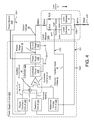
- FIG. 7 is a diagram that illustrates yet another power supply circuit 720 configured to deliver power from a power source 750 to a load module 730 (also can be referred to as a working device).
- the power supply circuit 720 includes a reference voltage circuit 722 (e.g., a bandgap reference circuit), a controller 724 , a power stage 726 , and an output stage 727 .
- the power supply circuit 720 is configured to manage (e.g., control, regulate) an output voltage 76 that is delivered to the load module 730 based on a reference voltage 72 , a feedback signal 77 , and an amplified ripple signal 79 . As shown in FIG.
- the feedback signal 77 and the amplified ripple signal 79 are combined (e.g., combined at an adder component 766 ) to produce an amplified feedback signal 75 .
- the signals can each be defined by one or more voltages that can change over time.
- the amplified ripple signal 79 (or component signals used to the produce the amplified ripple signal 79 ) can function as, or can be referred to as, an alternating current (AC) feedback signal
- the feedback signal 77 (or component signals used to the produce the feedback signal 77 ) can functions as, or can be referred to as, a direct current (DC) feedback signal.
- the AC feedback signal(s) and the DC feedback signal(s) are associated with different locations of the load module 730 .
- the power supply circuit 720 shown in FIG. 7 is identical to the power supply circuit 420 shown in FIG. 4 except for the configuration of the controller 724 .
- the controller 724 shown in FIG. 7 includes a hysteretic comparator 770 and an error amplifier 772 .
- the output of the hysteretic comparator 770 which receives the amplified ripple signal 79 , is combined (at the adder component 766 ) with the output of the error amplifier 772 , which receives the feedback signal 77 and the reference voltage 72 , to produce the amplified feedback signal 75 .
- the output of the error amplifier 772 can move (e.g., shift in an upward direction, shift in a downward direction) with movement in the reference ground voltage G 72 .
- the reference ground voltage G 72 can be directly received by the reference voltage circuit 722 without intervening circuitry (e.g., operational amplifiers, sense circuitry, etc.) and/or processing.
- different configurations of the power supply circuit shown in FIG. 1 , 4 , or 7 e.g., the controller 724 of the power supply circuit 720 ) can be implemented.
- Implementations of the various techniques described herein may be implemented in digital electronic circuitry, or in computer hardware, firmware, software, or in combinations of them. Portions of methods may be performed by, and an apparatus (e.g., the input power protection device, the power management device) may be implemented within, special purpose logic circuitry, e.g., an FPGA (field programmable gate array) or an ASIC (application-specific integrated circuit).
- an apparatus e.g., the input power protection device, the power management device
- special purpose logic circuitry e.g., an FPGA (field programmable gate array) or an ASIC (application-specific integrated circuit).
- Some implementations may include various semiconductor processing and/or packaging techniques. Some embodiments may be implemented using various types of semiconductor processing techniques associated with semiconductor substrates including, but not limited to, for example, Silicon (Si), Galium Arsenide (GaAs), Silicon Carbide (SiC), and/or so forth.
- semiconductor substrates including, but not limited to, Silicon (Si), Galium Arsenide (GaAs), Silicon Carbide (SiC), and/or so forth.
Landscapes
- Engineering & Computer Science (AREA)
- Power Engineering (AREA)
- Physics & Mathematics (AREA)
- Electromagnetism (AREA)
- General Physics & Mathematics (AREA)
- Radar, Positioning & Navigation (AREA)
- Automation & Control Theory (AREA)
- Dc-Dc Converters (AREA)
Abstract
Description
Claims (29)
Priority Applications (4)
| Application Number | Priority Date | Filing Date | Title |
|---|---|---|---|
| US13/216,522 US8633680B2 (en) | 2011-03-28 | 2011-08-24 | Differential sensing for voltage control in a power supply circuit |
| KR1020120031198A KR101960404B1 (en) | 2011-03-28 | 2012-03-27 | Differential sensing for voltage control in a power supply circuit |
| TW101110642A TWI521836B (en) | 2011-03-28 | 2012-03-27 | Apparatus and method for differential sensing for voltage control in a power supply circuit |
| CN201210085514.2A CN102710119B (en) | 2011-03-28 | 2012-03-28 | Voltage-controlled differential sensing in supply of electric power circuit |
Applications Claiming Priority (3)
| Application Number | Priority Date | Filing Date | Title |
|---|---|---|---|
| US201161468224P | 2011-03-28 | 2011-03-28 | |
| US201161472980P | 2011-04-07 | 2011-04-07 | |
| US13/216,522 US8633680B2 (en) | 2011-03-28 | 2011-08-24 | Differential sensing for voltage control in a power supply circuit |
Publications (2)
| Publication Number | Publication Date |
|---|---|
| US20120249094A1 US20120249094A1 (en) | 2012-10-04 |
| US8633680B2 true US8633680B2 (en) | 2014-01-21 |
Family
ID=46926338
Family Applications (1)
| Application Number | Title | Priority Date | Filing Date |
|---|---|---|---|
| US13/216,522 Active 2032-05-08 US8633680B2 (en) | 2011-03-28 | 2011-08-24 | Differential sensing for voltage control in a power supply circuit |
Country Status (4)
| Country | Link |
|---|---|
| US (1) | US8633680B2 (en) |
| KR (1) | KR101960404B1 (en) |
| CN (1) | CN102710119B (en) |
| TW (1) | TWI521836B (en) |
Cited By (4)
| Publication number | Priority date | Publication date | Assignee | Title |
|---|---|---|---|---|
| US9768695B2 (en) | 2015-05-12 | 2017-09-19 | Samsung Electronics Co., Ltd. | Power converting circuit and hysteresis buck converter with changing response characteristic based on transient state of output voltage |
| US10546082B1 (en) * | 2018-01-17 | 2020-01-28 | Mentor Graphics Corporation | Resistor network reduction for full-chip simulation of current density |
| TWI794315B (en) * | 2017-10-30 | 2023-03-01 | 美商瑞薩電子美國有限公司 | Low power hysteretic buck-boost dc-dc controller |
| US11693472B2 (en) | 2021-08-31 | 2023-07-04 | Apple Inc. | Multi-die power management in SoCs |
Families Citing this family (13)
| Publication number | Priority date | Publication date | Assignee | Title |
|---|---|---|---|---|
| US9541974B1 (en) * | 2013-03-15 | 2017-01-10 | Maxim Integrated Products, Inc. | Voltage transition technique for a voltage converter |
| CN104953816B (en) * | 2014-03-26 | 2017-11-17 | 华为技术有限公司 | Determine the method and device of dynamic regulation of voltage values of circuit resistances |
| US10833584B2 (en) | 2015-11-12 | 2020-11-10 | Empower Semiconductor, Inc. | Boot-strapping systems and techniques for circuits |
| US10630175B2 (en) * | 2016-08-03 | 2020-04-21 | Texas Instruments Incorporated | Pseudo current tracking for power supply regulation |
| JP6292325B1 (en) * | 2017-01-20 | 2018-03-14 | 日本電気株式会社 | Semiconductor integrated circuit, semiconductor system and method |
| TWI610515B (en) * | 2017-06-02 | 2018-01-01 | 國立交通大學 | Fuel cell system |
| US10236772B1 (en) * | 2018-02-09 | 2019-03-19 | Semiconductor Components Industries, Llc | Signal communication for circuit with floating ground |
| US10298114B1 (en) * | 2018-09-08 | 2019-05-21 | Shenzhen GOODIX Technology Co., Ltd. | Ripple detection and cancellation for voltage regulator circuits |
| CN112740506A (en) * | 2018-09-13 | 2021-04-30 | 松下知识产权经营株式会社 | Power supply device and motor control device provided with same |
| US11418120B2 (en) | 2018-12-26 | 2022-08-16 | Empower Semiconductor, Inc. | Deeply integrated voltage regulator architectures |
| DE112019006475T5 (en) | 2018-12-26 | 2021-09-30 | Empower Semiconductor, Inc. | Deeply integrated voltage regulator architectures |
| US12027977B2 (en) | 2021-04-19 | 2024-07-02 | Mediatek Singapore Pte. Ltd. | Voltage regulator using feedback loop circuit for accurately regulating output voltage when integration of error voltage is on hold |
| CN116545226B (en) * | 2023-07-06 | 2023-09-15 | 西安矽源半导体有限公司 | Resonance conversion circuit based on FPGA and method thereof |
Citations (7)
| Publication number | Priority date | Publication date | Assignee | Title |
|---|---|---|---|---|
| US5982160A (en) * | 1998-12-24 | 1999-11-09 | Harris Corporation | DC-to-DC converter with inductor current sensing and related methods |
| US6979985B2 (en) * | 2002-06-07 | 2005-12-27 | Renesas Technology Corp. | Switching power supply device and switching power supply system |
| US20070035281A1 (en) * | 2005-08-11 | 2007-02-15 | Renesas Technology Corp. | Switching regulator |
| US7759920B2 (en) * | 2006-12-20 | 2010-07-20 | Ricoh Company, Ltd. | Switching regulator and semiconductor device having the same |
| US7839130B2 (en) * | 2007-05-11 | 2010-11-23 | Ricoh Company, Ltd. | Switching regulator capable of preventing reverse current |
| US20120153723A1 (en) * | 2010-12-17 | 2012-06-21 | Nxp B.V. | Power supply circuit with shared functionality and method for operating the power supply circuit |
| US8373397B2 (en) * | 2009-11-17 | 2013-02-12 | Kabushiki Kaisha Toshiba | DC-DC converter and semiconductor integrated circuit |
Family Cites Families (1)
| Publication number | Priority date | Publication date | Assignee | Title |
|---|---|---|---|---|
| CN101499719A (en) * | 2008-02-03 | 2009-08-05 | 台湾类比科技股份有限公司 | Pulse width modulation controller and control method thereof |
-
2011
- 2011-08-24 US US13/216,522 patent/US8633680B2/en active Active
-
2012
- 2012-03-27 TW TW101110642A patent/TWI521836B/en active
- 2012-03-27 KR KR1020120031198A patent/KR101960404B1/en active IP Right Grant
- 2012-03-28 CN CN201210085514.2A patent/CN102710119B/en active Active
Patent Citations (8)
| Publication number | Priority date | Publication date | Assignee | Title |
|---|---|---|---|---|
| US5982160A (en) * | 1998-12-24 | 1999-11-09 | Harris Corporation | DC-to-DC converter with inductor current sensing and related methods |
| US6979985B2 (en) * | 2002-06-07 | 2005-12-27 | Renesas Technology Corp. | Switching power supply device and switching power supply system |
| US20070035281A1 (en) * | 2005-08-11 | 2007-02-15 | Renesas Technology Corp. | Switching regulator |
| US7492132B2 (en) * | 2005-08-11 | 2009-02-17 | Renesas Technology Corp. | Switching regulator |
| US7759920B2 (en) * | 2006-12-20 | 2010-07-20 | Ricoh Company, Ltd. | Switching regulator and semiconductor device having the same |
| US7839130B2 (en) * | 2007-05-11 | 2010-11-23 | Ricoh Company, Ltd. | Switching regulator capable of preventing reverse current |
| US8373397B2 (en) * | 2009-11-17 | 2013-02-12 | Kabushiki Kaisha Toshiba | DC-DC converter and semiconductor integrated circuit |
| US20120153723A1 (en) * | 2010-12-17 | 2012-06-21 | Nxp B.V. | Power supply circuit with shared functionality and method for operating the power supply circuit |
Non-Patent Citations (4)
| Title |
|---|
| "2.5A Step-Down Regulator with Remote Sense in 2mm ×2mm WLP", MAX8952, Maxim Integrated Products, Revision 1, Jun. 2011, pp. 1-31. |
| "6-Bit VID Controlled 2-4 Phase DC-DC Controller", Fairchild Semiconductor, FAN5019, Objective Specification FAN5019, Revision 0.0.4, Aug. 5, 2003, pp. 1-28. |
| "PWM DC/DC Controller with VID Inputs for Portable GPU Core-Voltage Regulator", intersil, ISL95870, ISL95870A, ISL95870B, FN6899.0, Dec. 22, 2009, pp. 1-29. |
| "Single Phase PWM Controller with Light-Load Efficiency Optimization", ST, L6738, Revision 0.74, Mar. 17, 2009, pp. 1-27. |
Cited By (7)
| Publication number | Priority date | Publication date | Assignee | Title |
|---|---|---|---|---|
| US9768695B2 (en) | 2015-05-12 | 2017-09-19 | Samsung Electronics Co., Ltd. | Power converting circuit and hysteresis buck converter with changing response characteristic based on transient state of output voltage |
| TWI794315B (en) * | 2017-10-30 | 2023-03-01 | 美商瑞薩電子美國有限公司 | Low power hysteretic buck-boost dc-dc controller |
| US11736011B2 (en) | 2017-10-30 | 2023-08-22 | Renesas Electronics America Inc. | Window comparator structure for low power hysteretic buck-boost DC-DC controller |
| US10546082B1 (en) * | 2018-01-17 | 2020-01-28 | Mentor Graphics Corporation | Resistor network reduction for full-chip simulation of current density |
| US11693472B2 (en) | 2021-08-31 | 2023-07-04 | Apple Inc. | Multi-die power management in SoCs |
| US11853140B2 (en) | 2021-08-31 | 2023-12-26 | Apple Inc. | Power management based on limiting hardware-forced power control |
| US11960341B2 (en) | 2021-08-31 | 2024-04-16 | Apple Inc. | Power delivery reduction scheme for SoC |
Also Published As
| Publication number | Publication date |
|---|---|
| TWI521836B (en) | 2016-02-11 |
| CN102710119A (en) | 2012-10-03 |
| US20120249094A1 (en) | 2012-10-04 |
| TW201320562A (en) | 2013-05-16 |
| KR20120110059A (en) | 2012-10-09 |
| CN102710119B (en) | 2016-09-14 |
| KR101960404B1 (en) | 2019-03-20 |
Similar Documents
| Publication | Publication Date | Title |
|---|---|---|
| US8633680B2 (en) | Differential sensing for voltage control in a power supply circuit | |
| US9454168B2 (en) | LDO regulator powered by its regulated output voltage for high PSRR | |
| US7570035B2 (en) | Voltage regulator with a hybrid control loop | |
| TWI431913B (en) | Current detection circuit and current mode switch regulator | |
| US9653982B2 (en) | Power supply systems and methods | |
| US7279875B2 (en) | High switching frequency DC-DC converter with fast response time | |
| US9966832B1 (en) | Predictive ripple-cancelling signal into error amplifier of switch mode power supply | |
| US8928303B2 (en) | Apparatus and methods for transient compensation of switching power regulators | |
| US7777464B2 (en) | Mixed type frequency compensating circuit and control circuit | |
| TW201618454A (en) | Multi-stage amplifier | |
| US10193449B2 (en) | Buck voltage converter | |
| US9817427B2 (en) | Static offset reduction in a current conveyor | |
| US8648639B2 (en) | Duty adjustment circuits and signal generation devices using the same | |
| US20240030817A1 (en) | Dynamic biasing circuit for main comparator to improve load-transient and line-transient performance of buck converter in 100% mode | |
| US8884595B2 (en) | Phase compensation circuit, semiconductor integrated circuit having phase compensation circuit, and power supply circuit having phase compensation circuit | |
| US9117507B2 (en) | Multistage voltage regulator circuit | |
| JP2009153249A (en) | Dc-dc converter | |
| JP2012016123A (en) | Dc-dc converter | |
| US20230314484A1 (en) | Current sensing for power converter | |
| US8013582B2 (en) | Voltage control circuit | |
| JP2014207820A (en) | Switching regulator and control circuit thereof, electronic apparatus using the same | |
| JP2012032940A (en) | Power supply control circuit | |
| US9367073B2 (en) | Voltage regulator | |
| KR20140006574A (en) | Voltage supply device | |
| US11848613B1 (en) | Automatic charge balancing between phases using voltage control loop in multiphase converter |
Legal Events
| Date | Code | Title | Description |
|---|---|---|---|
| AS | Assignment |
Owner name: FAIRCHILD SEMICONDUCTOR CORPORATION, CALIFORNIA Free format text: ASSIGNMENT OF ASSIGNORS INTEREST;ASSIGNORS:ZHAO, BIN;CORNISH, JACK;LEE, VICTOR;SIGNING DATES FROM 20110822 TO 20110823;REEL/FRAME:026800/0574 |
|
| STCF | Information on status: patent grant |
Free format text: PATENTED CASE |
|
| AS | Assignment |
Owner name: DEUTSCHE BANK AG NEW YORK BRANCH, AS COLLATERAL AGENT, NEW YORK Free format text: PATENT SECURITY AGREEMENT;ASSIGNOR:FAIRCHILD SEMICONDUCTOR CORPORATION;REEL/FRAME:040075/0644 Effective date: 20160916 Owner name: DEUTSCHE BANK AG NEW YORK BRANCH, AS COLLATERAL AG Free format text: PATENT SECURITY AGREEMENT;ASSIGNOR:FAIRCHILD SEMICONDUCTOR CORPORATION;REEL/FRAME:040075/0644 Effective date: 20160916 |
|
| FPAY | Fee payment |
Year of fee payment: 4 |
|
| MAFP | Maintenance fee payment |
Free format text: PAYMENT OF MAINTENANCE FEE, 8TH YEAR, LARGE ENTITY (ORIGINAL EVENT CODE: M1552); ENTITY STATUS OF PATENT OWNER: LARGE ENTITY Year of fee payment: 8 |
|
| AS | Assignment |
Owner name: SEMICONDUCTOR COMPONENTS INDUSTRIES, LLC, ARIZONA Free format text: ASSIGNMENT OF ASSIGNORS INTEREST;ASSIGNOR:FAIRCHILD SEMICONDUCTOR CORPORATION;REEL/FRAME:057694/0374 Effective date: 20210722 |
|
| AS | Assignment |
Owner name: FAIRCHILD SEMICONDUCTOR CORPORATION, ARIZONA Free format text: RELEASE BY SECURED PARTY;ASSIGNOR:DEUTSCHE BANK AG NEW YORK BRANCH;REEL/FRAME:057969/0206 Effective date: 20211027 |
|
| AS | Assignment |
Owner name: DEUTSCHE BANK AG NEW YORK BRANCH, AS COLLATERAL AGENT, NEW YORK Free format text: SECURITY INTEREST;ASSIGNOR:SEMICONDUCTOR COMPONENTS INDUSTRIES, LLC;REEL/FRAME:058871/0799 Effective date: 20211028 |
|
| AS | Assignment |
Owner name: FAIRCHILD SEMICONDUCTOR CORPORATION, ARIZONA Free format text: RELEASE OF SECURITY INTEREST IN PATENTS RECORDED AT REEL 040075, FRAME 0644;ASSIGNOR:DEUTSCHE BANK AG NEW YORK BRANCH, AS COLLATERAL AGENT;REEL/FRAME:064070/0536 Effective date: 20230622 Owner name: SEMICONDUCTOR COMPONENTS INDUSTRIES, LLC, ARIZONA Free format text: RELEASE OF SECURITY INTEREST IN PATENTS RECORDED AT REEL 040075, FRAME 0644;ASSIGNOR:DEUTSCHE BANK AG NEW YORK BRANCH, AS COLLATERAL AGENT;REEL/FRAME:064070/0536 Effective date: 20230622 |
|
| AS | Assignment |
Owner name: FAIRCHILD SEMICONDUCTOR CORPORATION, ARIZONA Free format text: RELEASE OF SECURITY INTEREST IN PATENTS RECORDED AT REEL 058871, FRAME 0799;ASSIGNOR:DEUTSCHE BANK AG NEW YORK BRANCH, AS COLLATERAL AGENT;REEL/FRAME:065653/0001 Effective date: 20230622 Owner name: SEMICONDUCTOR COMPONENTS INDUSTRIES, LLC, ARIZONA Free format text: RELEASE OF SECURITY INTEREST IN PATENTS RECORDED AT REEL 058871, FRAME 0799;ASSIGNOR:DEUTSCHE BANK AG NEW YORK BRANCH, AS COLLATERAL AGENT;REEL/FRAME:065653/0001 Effective date: 20230622 |