US8621923B2 - Humidity sensor - Google Patents
Humidity sensor Download PDFInfo
- Publication number
- US8621923B2 US8621923B2 US12/908,979 US90897910A US8621923B2 US 8621923 B2 US8621923 B2 US 8621923B2 US 90897910 A US90897910 A US 90897910A US 8621923 B2 US8621923 B2 US 8621923B2
- Authority
- US
- United States
- Prior art keywords
- sensor
- humidity
- voltage
- control electrode
- layer
- Prior art date
- Legal status (The legal status is an assumption and is not a legal conclusion. Google has not performed a legal analysis and makes no representation as to the accuracy of the status listed.)
- Expired - Fee Related, expires
Links
Images


Classifications
-
- G—PHYSICS
- G01—MEASURING; TESTING
- G01N—INVESTIGATING OR ANALYSING MATERIALS BY DETERMINING THEIR CHEMICAL OR PHYSICAL PROPERTIES
- G01N27/00—Investigating or analysing materials by the use of electric, electrochemical, or magnetic means
- G01N27/26—Investigating or analysing materials by the use of electric, electrochemical, or magnetic means by investigating electrochemical variables; by using electrolysis or electrophoresis
- G01N27/403—Cells and electrode assemblies
- G01N27/414—Ion-sensitive or chemical field-effect transistors, i.e. ISFETS or CHEMFETS
Definitions
- the invention relates to a humidity sensor which has, on a substrate, at least one voltage sensor with a sensor region and at least one control electrode that is connected to a signal source designed such that a variable control voltage can be applied to the control electrode, wherein a moisture-permeable sensor layer whose dielectric constant depends on humidity is located on the sensor region adjacent to the control electrode, wherein the control electrode is adjacent to the sensor layer in such a manner that the measured voltage signal of the voltage sensor depends on the control voltage and the humidity, and wherein the voltage sensor is connected to an analysis unit for ascertaining the humidity on the basis of the measured voltage signal.
- a humidity sensor of this nature is known from EP 1 176 418 A2.
- the humidity sensor has a semiconductor chip in which a field-effect transistor is integrated as the voltage sensor.
- the field-effect transistor has a drain and a source between which a channel region is formed as a voltage-sensitive sensor region.
- a gas-sensitive sensor layer that is polarizable independently of the humidity and whose dielectric constant depends on the humidity.
- the sensor layer is made of a porous, gas-permeable material.
- a control electrode Located on the sensor is a control electrode, which likewise is porous and gas-permeable and completely covers both the sensor layer and a passivation layer that is laterally contiguous therewith.
- the humidity sensor has the disadvantage that an additional fabrication step is required during its fabrication, after the application of the sensor layer on the channel region, in which a porous metallization is applied as the control electrode to the sensor layer and the passivation layer laterally contiguous therewith.
- the metallization must adhere to the sensor layer and the passivation layer. This results in certain restrictions in the choice of materials for the metallization and the sensor layer. It is also unfavorable that only porous, gas-permeable layers can be used as metallization.
- the control electrode is located laterally next to the sensor layer and/or beneath the sensor layer between it and the substrate, without covering the sensor layer.
- the sensor layer can thus be designed as a cover layer that stands in direct contact with the atmosphere surrounding the humidity sensor. Consequently, the control electrode can be made of a material that is impermeable, or only poorly permeable, to moisture. Nevertheless, the humidity sensor according to the invention permits a rapid response of the humidity measurement signal to a change in the humidity.
- the control electrode can surround the sensor region in the form of a ring.
- the variable control voltage or the variable voltage can act on the sensor layer in a better and more homogeneous fashion, for example in that dipoles located in the sensor region are aligned by the voltage change or are induced by charge displacement.
- This charge displacement which also is dependent on the humidity, can be capacitively detected by means of the voltage sensor.
- the sensor layer completely covers the control electrode.
- the measured voltage signal of the voltage sensor is then largely insensitive to contaminants occurring at the humidity sensor. Such contaminants are difficult to avoid, especially after the humidity sensor has been in service for a relatively long time. Moreover, the humidity sensor can then be manufactured more easily and more economically.
- An electrically insulating layer can be located between the control electrode and the sensor layer.
- the thickness of the insulating layer or the spacing between the control electrode and the sensor layer is chosen here such that the electric field created by the control voltage acts capacitively on the sensor layer through the insulating layer.
- the sensor layer in turn, is capacitively coupled to the sensor region of the voltage sensor. As a result of the insulating layer, the measured voltage signal is still less sensitive to contamination on the humidity sensor.
- the insulating layer can be a native insulating layer, which is produced by contact of the control electrode with atmospheric oxygen during fabrication of the humidity sensor.
- the sensor layer can be made of polymethyl methacrylate (PMMA) or contains polymethyl methacrylate (PMMA).
- PMMA polymethyl methacrylate
- PMMA polymethyl methacrylate
- the voltage sensor can be a field-effect transistor that has a semiconductor substrate of a first charge carrier type on which are located a drain and a source of a second charge carrier type, and when a channel region that forms the sensor region is provided between drain and source.
- the variable voltage can be measured in a high-resistance manner using the field-effect transistor.
- the channel region of the field-effect transistor is preferably located directly beneath the sensor layer, thereby allowing measurement signal extraction that is largely insensitive to EMC influences and also allowing the sensor to have compact dimensions.
- the sensor region is comprised of a preferably planar measurement electrode, which is connected by a conductive trace to the gate electrode of a field-effect transistor and/or an input of a high-resistance instrumentation amplifier.
- the channel region of the field-effect transistor or the instrumentation amplifier can also be located laterally next to the sensor region.
- the signal source is designed such that it can generate a control voltage with at least one jump, in particular a square-wave voltage.
- the voltage measurement signal of the voltage sensor can then be analyzed in a simple manner in the analysis unit.
- the invention is not restricted to the use of a control voltage that has a jump.
- the invention can also have an arbitrary signal shape deviating from a DC signal.
- the effect that the signal shape of the control voltage has on the voltage measurement signal must then be appropriately calculated out of the voltage measurement signal, for example by correlation of the voltage measurement signal with the control voltage.
- the signal source and the analysis unit can be integrated in the substrate.
- the humidity sensor is then still more economical to produce, and in addition allows very compact dimensions.
- FIG. 1 shows a cross-section through a first exemplary embodiment of a humidity sensor
- FIG. 2 shows a top view of the humidity sensor
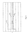
- FIG. 3 shows a graphical representation of two voltage measurement signals of the humidity sensor plotted for different relative humidities, during the application of a control voltage to a control electrode, where the time t is represented on the abscissa and the voltage measurement signal s or the control voltage is represented on the ordinate;
- FIG. 4 shows a cross-section through a second exemplary embodiment of the humidity sensor.
- a humidity sensor has a semiconductor chip 1 , which has a substrate 2 of a first charge carrier type. Integrated into the substrate 2 is a voltage sensor that is designed as a field-effect transistor. As is evident from FIG. 1 , the voltage sensor has a drain 3 and a source 4 of a second charge carrier type, which are set into the substrate 2 as wells. Located between the drain 3 and the source 4 is a channel region, which serves as the sensor region 5 for measuring a voltage change. Located on the substrate 2 is an electrically insulating layer 6 , which extends continuously over the drain 3 , the source 4 , and the sensor region 5 , except for places where electrical contact terminals are located. The insulating layer 6 can be an oxide layer, for example.
- a control electrode 7 made of an electrically conductive material is provided on the insulating layer 6 ; in the top view shown in FIG. 2 of the plane in which the substrate 2 extends, this control electrode is located laterally next to the sensor region 5 . It is clearly visible that the control electrode 7 is designed as an annular electrode that surrounds the sensor region 5 .
- the control electrode 7 is coated on its surface 8 facing away from the substrate 2 and on its inner circumferential surface 9 and its outer circumferential surface 10 with an electrically insulating layer 11 , which can be a native oxide layer, for example.
- a humidity-permeable sensor layer 12 Located on the insulating layer 6 above the sensor region 5 is a humidity-permeable sensor layer 12 whose dielectric constant is a function of humidity.
- the sensor layer 12 is preferably made of polymethyl methacrylate.
- the sensor layer 12 extends unbroken over the first surface region of the insulating layer 6 surrounded by the control electrode 7 , over the control electrode 7 , and over an approximately ring-shaped second surface region of the insulating layer 6 that surrounds the outside of the control electrode. It is evident in FIG. 1 that the control electrode 7 is completely covered on its surface 8 facing away from the substrate 2 and on its inner circumferential surface 9 and its outer circumferential surface 10 by the sensor layer 12 . Here, the control electrode 7 is electrically insulated from the sensor layer 12 by the insulating layer 11 .
- the control electrode 7 is connected to a signal source 19 by a conductive trace integrated into the semiconductor chip 1 .
- a variable control voltage preferably a square-wave signal with predetermined frequency and predetermined amplitude, can be applied between the substrate 2 and the control electrode 7 .
- the control electrode 7 is adjacent to the sensor layer 12 in such a manner that the electric field created by the control voltage extends through the insulating layer 11 into the sensor layer 12 and polarizes charge carriers therein.
- this polarization which depends on the control voltage and the humidity, is measured capacitively in the form of a measured voltage signal 13 a , 13 b ( FIG. 3 ).
- the voltage sensor is connected to an analysis unit 20 .
- This analysis unit 20 may be integrated in the semiconductor chip 1 .
- the measured voltage signal 13 a , 13 b also has a corresponding jump. It can also be seen that with a constant shape 14 of the control voltage, the measured voltage signal 13 a , 13 b is shifted by an offset 15 when the relative humidity changes. With an increase in the humidity, the value of the measured voltage signal 13 a , 13 b increases, and with a decrease in the humidity, the value of the measured voltage signal 13 a , 13 b decreases.
- Reference values for the offset 15 are prepared as a function of the relative humidity, for example in the form of characteristic curves or in the form of a family of curves for which sampling points are stored.
- the relative humidity can then be determined using the measured voltage signal 13 a , 13 b and the reference values, for example in order to generate an analog signal proportional to the relative humidity and/or a corresponding digital signal in the analysis unit.
- the sensor region 5 ′ is composed of a planar measurement electrode that is located beneath the sensor layer 12 at a distance from the control electrode 7 and is connected by a conductive trace 16 to a gate electrode 18 that is located over a channel region 17 of a field-effect transistor placed between a drain 3 ′ and a source 4 ′. It is clearly visible that the field-effect transistor is integrated into the substrate 2 of the semiconductor chip 1 laterally next to the arrangement comprising the sensor region 5 ′, the control electrode 7 , the insulating layer 11 and the sensor layer 12 .
Landscapes
- Life Sciences & Earth Sciences (AREA)
- Chemical & Material Sciences (AREA)
- Health & Medical Sciences (AREA)
- Physics & Mathematics (AREA)
- Molecular Biology (AREA)
- Microelectronics & Electronic Packaging (AREA)
- Chemical Kinetics & Catalysis (AREA)
- Electrochemistry (AREA)
- Engineering & Computer Science (AREA)
- Analytical Chemistry (AREA)
- Biochemistry (AREA)
- General Health & Medical Sciences (AREA)
- General Physics & Mathematics (AREA)
- Immunology (AREA)
- Pathology (AREA)
- Investigating Or Analyzing Materials By The Use Of Electric Means (AREA)
Abstract
Description
Claims (9)
Applications Claiming Priority (3)
| Application Number | Priority Date | Filing Date | Title |
|---|---|---|---|
| EPEP09013311.7 | 2009-10-21 | ||
| EP09013311.7A EP2315013B1 (en) | 2009-10-21 | 2009-10-21 | Humidity sensor |
| EP09013311 | 2009-10-21 |
Publications (2)
| Publication Number | Publication Date |
|---|---|
| US20110088466A1 US20110088466A1 (en) | 2011-04-21 |
| US8621923B2 true US8621923B2 (en) | 2014-01-07 |
Family
ID=42045352
Family Applications (1)
| Application Number | Title | Priority Date | Filing Date |
|---|---|---|---|
| US12/908,979 Expired - Fee Related US8621923B2 (en) | 2009-10-21 | 2010-10-21 | Humidity sensor |
Country Status (3)
| Country | Link |
|---|---|
| US (1) | US8621923B2 (en) |
| EP (1) | EP2315013B1 (en) |
| CN (1) | CN102043000B (en) |
Cited By (1)
| Publication number | Priority date | Publication date | Assignee | Title |
|---|---|---|---|---|
| US11047753B2 (en) | 2018-12-27 | 2021-06-29 | Therm-O-Disc, Incorporated | Pressure sensor assembly and method for manufacturing a pressure sensor assembly |
Families Citing this family (4)
| Publication number | Priority date | Publication date | Assignee | Title |
|---|---|---|---|---|
| EP2174122A2 (en) * | 2007-06-08 | 2010-04-14 | Bharath R Takulapalli | Nano structured field effect sensor and methods of forming and using same |
| US9341592B2 (en) | 2012-04-09 | 2016-05-17 | Bharath Takulapalli | Field effect transistor, device including the transistor, and methods of forming and using same |
| WO2017184790A1 (en) | 2016-04-19 | 2017-10-26 | Takulapalli Bharath | Nanopore sensor, structure and device including the sensor, and methods of forming and using same |
| WO2019107165A1 (en) * | 2017-11-30 | 2019-06-06 | 東レ株式会社 | Circuit, detector, wireless communication device, moisture sensing system, diaper, notification system, and circuit manufacturing method |
Citations (13)
| Publication number | Priority date | Publication date | Assignee | Title |
|---|---|---|---|---|
| US4423371A (en) | 1981-09-03 | 1983-12-27 | Massachusetts Institute Of Technology | Methods and apparatus for microdielectrometry |
| JPH01124755A (en) * | 1987-11-10 | 1989-05-17 | Fujikura Ltd | Humidity sensor made of thin organic high-polymer film |
| US4920451A (en) * | 1988-05-23 | 1990-04-24 | Yamatake-Honeywell Co., Ltd. | Moisture-sensitive element |
| JPH03137555A (en) * | 1989-10-24 | 1991-06-12 | Yamatake Honeywell Co Ltd | Humidity-sensitive element |
| JP3137555B2 (en) * | 1995-05-30 | 2001-02-26 | 富士写真光機株式会社 | Distance measuring device |
| EP1176418A2 (en) | 2000-07-25 | 2002-01-30 | Siemens Aktiengesellschaft | Potential controlled gas sensor |
| US6615659B2 (en) * | 2001-03-13 | 2003-09-09 | Tdk Corporation | Humidity sensor and method for manufacturing the same |
| CN1445538A (en) | 2002-03-20 | 2003-10-01 | 株式会社电装 | Capacitance humidity sensor with passivated layer |
| US20040194534A1 (en) * | 2002-06-03 | 2004-10-07 | Porter Timothy L. | Hybrid microcantilever sensors |
| WO2008122390A1 (en) | 2007-04-05 | 2008-10-16 | Micronas Gmbh | Moisture sensor and method for measuring moisture of a gas-phase medium |
| US20090078026A1 (en) * | 2007-06-22 | 2009-03-26 | Micronas Gmbh | Gas Sensor |
| US20090246084A1 (en) * | 2008-03-26 | 2009-10-01 | Micronas Gmbh | Gas Sensor |
| US8291745B2 (en) * | 2008-07-02 | 2012-10-23 | Stichting Imec Nederland | Analyte sensing device |
Family Cites Families (2)
| Publication number | Priority date | Publication date | Assignee | Title |
|---|---|---|---|---|
| CN2055247U (en) * | 1989-05-06 | 1990-03-28 | 山东建筑工程学院 | High precision temp. and humidity sensor |
| CN2080670U (en) * | 1990-11-27 | 1991-07-10 | 北京工业大学 | Capacitance type organic film humidity sensor |
-
2009
- 2009-10-21 EP EP09013311.7A patent/EP2315013B1/en active Active
-
2010
- 2010-10-15 CN CN201010511712.1A patent/CN102043000B/en active Active
- 2010-10-21 US US12/908,979 patent/US8621923B2/en not_active Expired - Fee Related
Patent Citations (14)
| Publication number | Priority date | Publication date | Assignee | Title |
|---|---|---|---|---|
| US4423371A (en) | 1981-09-03 | 1983-12-27 | Massachusetts Institute Of Technology | Methods and apparatus for microdielectrometry |
| JPH01124755A (en) * | 1987-11-10 | 1989-05-17 | Fujikura Ltd | Humidity sensor made of thin organic high-polymer film |
| US4920451A (en) * | 1988-05-23 | 1990-04-24 | Yamatake-Honeywell Co., Ltd. | Moisture-sensitive element |
| JPH03137555A (en) * | 1989-10-24 | 1991-06-12 | Yamatake Honeywell Co Ltd | Humidity-sensitive element |
| JP3137555B2 (en) * | 1995-05-30 | 2001-02-26 | 富士写真光機株式会社 | Distance measuring device |
| EP1176418A2 (en) | 2000-07-25 | 2002-01-30 | Siemens Aktiengesellschaft | Potential controlled gas sensor |
| US6615659B2 (en) * | 2001-03-13 | 2003-09-09 | Tdk Corporation | Humidity sensor and method for manufacturing the same |
| CN1445538A (en) | 2002-03-20 | 2003-10-01 | 株式会社电装 | Capacitance humidity sensor with passivated layer |
| US20040194534A1 (en) * | 2002-06-03 | 2004-10-07 | Porter Timothy L. | Hybrid microcantilever sensors |
| WO2008122390A1 (en) | 2007-04-05 | 2008-10-16 | Micronas Gmbh | Moisture sensor and method for measuring moisture of a gas-phase medium |
| US20100176826A1 (en) | 2007-04-05 | 2010-07-15 | Micronas Gmbh | Moisture Sensor and Method for Measuring Moisture of a Gas-Phase Medium |
| US20090078026A1 (en) * | 2007-06-22 | 2009-03-26 | Micronas Gmbh | Gas Sensor |
| US20090246084A1 (en) * | 2008-03-26 | 2009-10-01 | Micronas Gmbh | Gas Sensor |
| US8291745B2 (en) * | 2008-07-02 | 2012-10-23 | Stichting Imec Nederland | Analyte sensing device |
Non-Patent Citations (2)
| Title |
|---|
| Lee S P et al: "Humidity sensitive field effect transistors" Sensors and Actuators B, Elsevier Sequoia S.A., Lausanne, CH, Bd. 35, Nr. 1, Sep. 1, 1996, Seiten 80-84, XP004049735 ISSN: 0925-4005 DOI: 10. 1016/S0925-4005 (96) 02018-7. |
| Marquardt G: "Feuchtigkeitsempfindliche Feldeffekttransistoren" Wissenschaftlichezeitschrift der Technischen Hochschule Karl-Marx Stadt, Technische Universitaet Chemnitz, DE, Bd. 25, Nr. 6, Jan. 1, 1983, Seiten 884-887, XP009131757 ISSN: 0372-7610. |
Cited By (1)
| Publication number | Priority date | Publication date | Assignee | Title |
|---|---|---|---|---|
| US11047753B2 (en) | 2018-12-27 | 2021-06-29 | Therm-O-Disc, Incorporated | Pressure sensor assembly and method for manufacturing a pressure sensor assembly |
Also Published As
| Publication number | Publication date |
|---|---|
| US20110088466A1 (en) | 2011-04-21 |
| CN102043000B (en) | 2015-01-21 |
| EP2315013A1 (en) | 2011-04-27 |
| EP2315013B1 (en) | 2014-06-18 |
| CN102043000A (en) | 2011-05-04 |
Similar Documents
| Publication | Publication Date | Title |
|---|---|---|
| US11008611B2 (en) | Double gate ion sensitive field effect transistor | |
| US9518953B2 (en) | Ion sensitive detector | |
| US8860442B2 (en) | Method of determining a sensitivity of a biosensor arrangement, and biosensor sensitivity determining system | |
| US4397714A (en) | System for measuring the concentration of chemical substances | |
| CN107589165B (en) | Biosensor pixel circuit with amplification | |
| US8621923B2 (en) | Humidity sensor | |
| KR101322354B1 (en) | Humidity sensor, humidity sensing method and transistor therefor | |
| EP3217167B1 (en) | Humidity sensors with transistor structures and piezoelectric layer | |
| EP3206027B1 (en) | Sensor chip comprising electrostatic discharge protection element | |
| KR20200080481A (en) | Gas Sensor | |
| CN106959330B (en) | Integrated ion sensing apparatus and method | |
| US7918123B2 (en) | Gas sensor | |
| US7946153B2 (en) | Method for measuring gases and/or minimizing cross sensitivity in FET-based gas sensors | |
| US4816888A (en) | Sensor | |
| US8324913B2 (en) | Moisture sensor and method for measuring moisture of a gas-phase medium | |
| WO2020240942A1 (en) | Odor sensor and odor sensing method | |
| WO2019131564A1 (en) | Measurement instrument for chemical/physical phenomena and method for manufacturing same | |
| NL2011845C2 (en) | A capacitive sensor for humidity and/or ammonia sensing. | |
| US9103773B2 (en) | Capacitive element sensor and method for manufacturing same | |
| KR101729685B1 (en) | Method and appartus for detecting ion concentration | |
| CN102112868B (en) | Gas sensor | |
| EP3845895A1 (en) | Multi-sensing capacitive sensors | |
| Duarte et al. | Back Gate Bias Influence on BESOI ISFET Sensitivity | |
| US20260029362A1 (en) | Sensor device and corresponding methods | |
| US7326974B2 (en) | Sensor for measuring a gas concentration or ion concentration |
Legal Events
| Date | Code | Title | Description |
|---|---|---|---|
| AS | Assignment |
Owner name: MICRONAS GMBH, GERMANY Free format text: ASSIGNMENT OF ASSIGNORS INTEREST;ASSIGNOR:FRERICHS, HEINZ-PETER;REEL/FRAME:025575/0380 Effective date: 20101110 |
|
| FEPP | Fee payment procedure |
Free format text: PAYOR NUMBER ASSIGNED (ORIGINAL EVENT CODE: ASPN); ENTITY STATUS OF PATENT OWNER: LARGE ENTITY |
|
| STCF | Information on status: patent grant |
Free format text: PATENTED CASE |
|
| AS | Assignment |
Owner name: TDK-MICRONAS GMBH, GERMANY Free format text: CHANGE OF NAME;ASSIGNOR:MICRONAS GMBH;REEL/FRAME:041901/0191 Effective date: 20161212 |
|
| FPAY | Fee payment |
Year of fee payment: 4 |
|
| MAFP | Maintenance fee payment |
Free format text: PAYMENT OF MAINTENANCE FEE, 8TH YEAR, LARGE ENTITY (ORIGINAL EVENT CODE: M1552); ENTITY STATUS OF PATENT OWNER: LARGE ENTITY Year of fee payment: 8 |
|
| FEPP | Fee payment procedure |
Free format text: MAINTENANCE FEE REMINDER MAILED (ORIGINAL EVENT CODE: REM.); ENTITY STATUS OF PATENT OWNER: LARGE ENTITY |
|
| LAPS | Lapse for failure to pay maintenance fees |
Free format text: PATENT EXPIRED FOR FAILURE TO PAY MAINTENANCE FEES (ORIGINAL EVENT CODE: EXP.); ENTITY STATUS OF PATENT OWNER: LARGE ENTITY |
|
| STCH | Information on status: patent discontinuation |
Free format text: PATENT EXPIRED DUE TO NONPAYMENT OF MAINTENANCE FEES UNDER 37 CFR 1.362 |
|
| FP | Lapsed due to failure to pay maintenance fee |
Effective date: 20260107 |