US8618794B2 - Detecting inductive objects using inputs of integrated circuit device - Google Patents
Detecting inductive objects using inputs of integrated circuit device Download PDFInfo
- Publication number
- US8618794B2 US8618794B2 US12/848,071 US84807110A US8618794B2 US 8618794 B2 US8618794 B2 US 8618794B2 US 84807110 A US84807110 A US 84807110A US 8618794 B2 US8618794 B2 US 8618794B2
- Authority
- US
- United States
- Prior art keywords
- waveform
- environment
- emf
- digital
- timer
- Prior art date
- Legal status (The legal status is an assumption and is not a legal conclusion. Google has not performed a legal analysis and makes no representation as to the accuracy of the status listed.)
- Active, expires
Links
Images


Classifications
-
- G—PHYSICS
- G01—MEASURING; TESTING
- G01R—MEASURING ELECTRIC VARIABLES; MEASURING MAGNETIC VARIABLES
- G01R33/00—Arrangements or instruments for measuring magnetic variables
- G01R33/02—Measuring direction or magnitude of magnetic fields or magnetic flux
- G01R33/028—Electrodynamic magnetometers
-
- G—PHYSICS
- G01—MEASURING; TESTING
- G01R—MEASURING ELECTRIC VARIABLES; MEASURING MAGNETIC VARIABLES
- G01R33/00—Arrangements or instruments for measuring magnetic variables
- G01R33/0023—Electronic aspects, e.g. circuits for stimulation, evaluation, control; Treating the measured signals; calibration
- G01R33/0029—Treating the measured signals, e.g. removing offset or noise
Definitions
- This subject matter is generally related to electronics, and more particularly to detecting inductive objects in proximity to a sensor coil.
- a conventional sensor for measuring changes in an EMF environment is an inductor-capacitor (“LC”) oscillator circuit.
- the LC circuit can be charged by running current through it, and then letting the LC circuit oscillate freely.
- the resulting oscillation of energy creates an oscillating waveform, which can be observed by an application.
- the relative dampening of this waveform reflects changes in the perceived inductance of the coil in the LC circuit.
- the LC oscillator dissipates its energy faster because of the inductive coupling the coil forms with the metallic object.
- the magnetic coupling results in more rapid decay of the waveform envelope.
- the decay or fall off of the waveform envelope can be quantified to produce an inductive sensor signal.
- a conventional approach for measuring changes in an EMF environment uses an Analog Comparator with a tuneable reference level often generated by a digital-to-analog converter circuit (“DAC”).
- the analog comparator can be used to compare the waveform to the DAC-generated reference, and a mechanism then counts the number of times the oscillating waveform and reference voltage intersect. This count can be used as the inductive sensor's signal.
- a system for detecting inductive objects includes an inductive sensor circuit for detecting changes in an EMF environment and an integrated circuit (“IC”) device.
- the inductive sensor circuit generates an oscillating analog waveform with an envelope that indicates changes in the EMF environment.
- the oscillating waveform is coupled to the digital input pin of the IC device.
- a digital interface circuit in the IC device is coupled to the digital input pin and is configured for detecting if the oscillating waveform exceeds first and second threshold voltage levels.
- the detecting results in a digital pulse which represents the inductive sensor circuit signal.
- an application can measure changes in the EMF environment.
- the analog waveform generated by the inductive sensor circuit can be input to a timer input capture pin of the IC device.
- a timer module in the IC device can be programmed to store the associated timer value in a register of the IC device each time the input toggles (e.g., a zero crossing event).
- the timer module can be programmed to give a wake up signal after a predetermined time, and then have the device read the new sensor value from the timer input capture register.
- the predetermined time can be set long enough for the oscillating waveform envelope to fall within a hysteresis band of the timer input capture pin.
- the last time capture event will trigger earlier due to a smaller envelope amplitude in the oscillating waveform.
- the earlier capture time indicates a change in the EMF environment, and if this change is above a given threshold it constitutes a sensor detect state.
- a system for detecting changes in an EMF environment includes an inductive sensor circuit and an integrated circuit device.
- the inductive sensor circuit is configured to generate an oscillating analog waveform having an envelope that decays in response to a change in an electromagnetic field environment.
- the integrated circuit device is coupled to the inductive sensor circuit through a digital input pin.
- the integrated circuit device includes digital interface circuitry coupled to the digital input pin.
- the digital interface circuitry is configured to compare the oscillating waveform with first and second threshold levels, where the second threshold level is less than the first threshold level, and for outputting a digital pulse based on the comparing.
- a processor is coupled to the digital interface circuitry. The processor is configured to receive the digital pulse and to determine a change in the EMF environment based on the digital pulse.
- a system for detecting changes in an electromagnetic field environment field environment includes an inductive sensor circuit and an integrated circuit device.
- the inductive sensor circuit is configured to generate an oscillating analog waveform having an envelope that decays in response to a change in an electromagnetic field environment.
- the integrated circuit device is coupled to the inductive sensor circuit through a timer input capture pin.
- the integrated circuit device includes interface circuitry coupled to the timer input capture pin, a timer and a register.
- the interface circuitry is configured to store a current time value generated by the timer each time the waveform crosses a threshold.
- a processor is coupled to the interface circuitry and configured to retrieve a last stored time value after a time period expires, and to determine a change in the EMF environment based on the last stored time value.
- a method of detecting changes in an electromagnetic field environment field (“EMF”) environment includes: generating an oscillating analog waveform having an envelope that decays in response to a change in an electromagnetic field environment; coupling the waveform to a digital input pin of an integrated circuit device; processing the waveform to provide a digital pulse, the processing including using a digital interface circuit associated with the digital input pin to compare the oscillating waveform with first and second threshold levels, where the second threshold level is less than the first threshold level; and determining a change in the EMF environment based on the digital pulse.
- EMF electromagnetic field environment field
- a method of detecting changes in an electromagnetic field environment field (“EMF”) environment includes: generating an oscillating analog waveform having an envelope that decays in response to a change in an electromagnetic field environment; coupling the waveform to a timer input capture pin of an integrated circuit device; starting a timer, where the timer is to run for a time period; storing a current time value of the timer each time the waveform crosses a threshold value; determining that the timer has exceed the time period; and determining a change in the EMF environment based on a last stored time value.
- Using the digital input pin and existing digital interface circuitry of an IC to detect changes in an EMF environment can result in a simple inexpensive circuit design that can be easily adapted to other applications.
- Using the timer input capture pin provides an additional advantage of allowing the processor of the IC to enter sleep mode while running the timer.
- FIG. 1A is a schematic diagram of an inductive sensor circuit.
- FIG. 1B illustrates an oscillating waveform generated by the inductive sensor circuit of FIG. 1 .
- FIG. 1C illustrates a conventional method of detecting a change in the EMF environment based on the waveform using analog components.
- FIG. 2 illustrates generating a digital pulse from an oscillating waveform using the digital input of an IC device.
- FIG. 3 is a block diagram of an exemplary IC device with digital input and timer input capture pins, and corresponding circuitry for detecting changes in EMF environments from an oscillating waveform.
- FIG. 4 is a schematic diagram of an exemplary digital interface circuit for generating a digital pulse from an oscillating waveform.
- FIG. 5 is a flow diagram of an exemplary process for detecting changes in an EMF environment using a digital input pin.
- FIG. 6 is a flow diagram of an exemplary process for detecting changes in an EMF environment using a timer input capture pin.
- FIG. 1A is a schematic diagram of inductive sensor circuit 100 .
- Sensor circuit 100 is an LC circuit including an inductor L, capacitor C and resistor R 1 .
- Sensor circuit 100 includes a drive input pin (DRIVE_PIN) and sensor output pin (SENSOR_PIN).
- the values of L, C and R 1 can be selected to cause the sensor circuit 100 to oscillate when driven by a drive current applied to DRIVE_PIN.
- the resulting oscillation of energy between the L and C creates a waveform which can be observed by an application.
- the inductor or “coil” L is placed near a magnetic material the perceived inductance of the sensor circuit 100 changes, resulting in a dissipation of energy.
- the dissipation of energy is reflected in a decay of the envelope of the waveform over time. A more rapid decay in the envelope of the oscillating waveform indicates a change in the EMF environment of the coil.
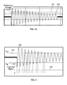
- FIG. 1B illustrates an oscillating waveform generated by the inductive sensor circuit 100 of FIG. 1 .
- a first waveform 102 occurs when the coil is not in proximity to a metallic object.
- a second waveform 104 occurs when the coil is in proximity of a metallic object.
- the relative dampening of the waveforms 102 , 104 reflects the changes in the perceived inductance, L, of the coil.
- L perceived inductance
- FIG. 1C illustrates a conventional method of detecting a change in the EMF environment based on an oscillating waveform 108 using analog components.
- a DAC is used to create a reference voltage 106 that intersects the oscillating waveform 108 at some predetermined level, as shown in FIG. 1C .
- Analog Comparator (“AC”) can be used to compare the waveform 108 to the DAC-generated reference voltage 106 , and a mechanism (e.g., a counter), then counts the number of times the oscillating waveform 108 and DAC-generated reference voltage 106 intersect. This count then becomes the sensor output signal that can be used by an application to detect changes in an EMF environment.
- AC Analog Comparator
- FIG. 2 illustrates generating a digital pulse 206 from an oscillating waveform 200 using the digital input of an IC device.
- the implicit voltage comparison commonly provided by a digital input pin of a commercially available IC device can be used to generate the digital pulse 206 that can be used by an application to detect changes in an EMF environment.
- a digital input pin will be coupled to a digital interface circuit that is configured to receive the digital input signal 200 . Because the digital input signal 200 may have been subjected to noise or hysteresis, the digital interface circuit compares the digital input signal 200 with threshold voltage levels 202 , 204 to register the digital input signal 200 as logical high or logical low.
- the digital input signal 200 can register as a logic “high” or “one” when the voltage of the digital input signal 200 on the digital input pin is higher than a first threshold level 202 (e.g., 3.6 Volts), also denoted as V IH in FIG. 2 . Because of hysteresis, the voltage level on the digital input pin has to drop below a second threshold level 204 (e.g., 0.9 Volts), also denoted as V IL in FIG. 2 , before it registers as a digital low or “zero.”
- a first threshold level 202 e.g., 3.6 Volts
- V IH 3.6 Volts
- the operation of the digital interface can be leveraged to create a simple, yet effective, voltage comparator.
- the waveform envelope from the second circuit 100 is wide enough to encompass both V IH and V IL , connecting the waveform to a digital input pin of the IC device will convert the waveform into the digital pulse 206 .
- the number of times the digital pulse 206 toggles from high to low or back again can be counted (e.g., by a software counter implemented in the IC device), thus creating the desired inductive sensor signal without using any analog components or adding additional digital components.
- the number of toggles will depend on the amplitude of the envelope, a faster dissipating envelope will mean that there are fewer toggles on the digital I/O pin.
- the values of V IH and V IL may not be calibrated, and can vary between IC devices. The lack of calibration is not a problem since it is the relative changes to the waveform that are used to determine changes in the inductive sensor signal.
- FIG. 3 is a block diagram of an exemplary IC device 300 with digital input and timer input capture pins, and corresponding circuitry for detecting changes in EMF environments from an oscillating waveform.
- FIG. 3 illustrates two possible options for using input pins of an IC device for detecting changes in EMF environments from an oscillating waveform.
- a first option A uses a digital input pin and a second option B uses a timer input capture pin.
- both options A and B can be used where one option can be used to confirm the accuracy of the other option or for other reasons (e.g., option B is used only in low power sleep mode).
- IC device 300 can include digital input pin 302 , digital interface circuit 304 and processor 306 .
- Processor 306 can include digital counter 308 .
- Digital counter 308 can be located elsewhere in IC device 300 , external to IC device 300 or implemented in software.
- IC device 300 can be any IC device with a digital input pin that performs a threshold comparison as described in reference to FIG. 2 (e.g., a microcontroller).
- an oscillating analog waveform is coupled to digital input pin 302 .
- the digital interface circuit 304 compares the waveform with first and second threshold levels and generates a digital pulse based on the comparing.
- the digital pulse can then be processed by processor 308 , which uses counter 306 to count the number of times the digital pulse toggles from high to low or back again.
- the count of counter 306 can be used to determine whether the coil of sensor circuit 100 is in proximity to a metallic object.
- IC device 300 includes timer input capture pin 310 , interface circuit 312 and processor 306 .
- Interface circuit 312 can include timer module 314 and register 316 .
- Timer module 314 and register 316 can also be included in processor 306 or part of another circuit in IC device 300 .
- Timer module 314 and register 316 can also be located outside of IC device 300 .
- an oscillating analog waveform is coupled to time input capture pin 310 .
- Timer 314 can be started and allowed to run for a defined (e.g., programmed) time period. For example, a time period can be programmed that is long enough for the oscillating waveform envelope to fall within a hysteresis band of the digital input pin.
- Processor 306 can be programmed to store an associated timer value in register 316 each time the oscillating waveform crosses a threshold level. For example, the current time value of timer 314 can be stored in register 316 each time a zero crossing occurs (waveform goes from positive to negative or drops below zero voltage) during the defined time period.
- the last stored time value can be compared to a reference time value to determine if the coil of sensor circuit 100 is in proximity to a metallic object.
- the reference time value can be determined empirically by running the system without a metallic object, and storing the resulting last time value as a reference value. For example, if the envelope has decayed due to a change in the perceived inductance of sensor circuit 100 , the last time value captured and stored in register 316 will be less (earlier) than the reference time value.
- Using the timer input capture pin 310 allows processor 306 to enter sleep mode while timer 314 is running.
- FIG. 4 is a simplified schematic diagram of an exemplary digital interface circuit 304 for generating a digital pulse from an oscillating waveform.
- a digital interface circuit 304 can include diodes 402 , 404 , capacitance 406 and transistor 408 .
- the output of circuit 304 is a sequence of digital pulses, as illustrated in FIG. 2 .
- Other circuit configurations with more or fewer components are also possible.
- FIG. 5 is a flow diagram of an exemplary process 500 for detecting changes in an EMF environment using a digital input pin.
- Process 500 can be performed by processor 306 in FIG. 3 .
- process 500 begins by generating an oscillating analog waveform having an envelope that decays in response to a change in an EMF environment ( 502 ).
- sensor circuit 100 can generate this waveform.
- the waveform is coupled to a digital input pin of an IC device ( 504 ).
- the SENSOR_PIN can be electrically connected with a circuitry trace or wire to digital input pin 302 of IC device 300 .
- Digital input pin 302 can be coupled to a digital interface circuit that processes the waveform to provide a digital pulse ( 506 ).
- the waveform can be compared with first and second threshold levels, where the second level is less than the first level.
- the existing digital interface circuit often used with a digital input of an IC device can be leveraged to perform the comparing and to set the threshold levels, thus avoiding the need to use analog components or add digital components.
- a change in the EMF environment can be determined based on the digital pulses ( 508 ). For example, a counter can count the number of times the digital pulse toggles from high to low and back again to determine if the coil of the sensor is in proximity to a metallic objects.
- a signal can be sent to the processor.
- the processor can retrieve the number of pulses, and report it to the main application (e.g., software application) for processing. In the case of a software counter this process becomes trivial by not using signals or interrupts.
- FIG. 6 is a flow diagram of an exemplary process 600 for detecting changes in an EMF environment using a timer input capture pin.
- Process 600 can be performed by processor 306 in FIG. 3 .
- process 600 begins by generating an oscillating analog waveform having an envelope that decays in response to a change in an EMF environment ( 602 ).
- sensor circuit 100 can generate this waveform.
- the waveform is coupled to a timer input capture pin of an IC device ( 604 ).
- the SENSOR_PIN of sensor circuit 100 can be electrically connected with a circuitry trace or wire to timer input capture pin 310 of IC device 300 .
- a timer is started and allowed to run for a time period ( 606 ).
- the time period can be long enough for the envelope of the oscillating waveform to fall within a hysteresis band of the digital input pin.
- the current time value of the timer is stored each time the waveform crosses a threshold level or toggles ( 608 ).
- the time value can be stored in register 316 in IC device 300 .
- Expiration of the time period is determined ( 610 ).
- processor 306 in the IC device 300 may receive a signal or interrupt from timer 312 when the time period has expired.
- Processor 300 can also reset timer 312 for a next time period.
- a change in the EMF environment can be determined based on the last stored time value ( 612 ).
- processor 300 can receive in an interrupt form timer 312 , and in response, processor 312 can retrieve the last time value stored register 316 . If the last stored time value is less than a reference time value (e.g., empirically determined time value), then an application can be alerted that a change to the EMF environment.
- a reference time value e.g., empirically determined time value
Landscapes
- Physics & Mathematics (AREA)
- Condensed Matter Physics & Semiconductors (AREA)
- General Physics & Mathematics (AREA)
- Electronic Switches (AREA)
- Acyclic And Carbocyclic Compounds In Medicinal Compositions (AREA)
Abstract
Description
Claims (14)
Priority Applications (1)
| Application Number | Priority Date | Filing Date | Title |
|---|---|---|---|
| US12/848,071 US8618794B2 (en) | 2010-07-30 | 2010-07-30 | Detecting inductive objects using inputs of integrated circuit device |
Applications Claiming Priority (1)
| Application Number | Priority Date | Filing Date | Title |
|---|---|---|---|
| US12/848,071 US8618794B2 (en) | 2010-07-30 | 2010-07-30 | Detecting inductive objects using inputs of integrated circuit device |
Publications (2)
| Publication Number | Publication Date |
|---|---|
| US20120025813A1 US20120025813A1 (en) | 2012-02-02 |
| US8618794B2 true US8618794B2 (en) | 2013-12-31 |
Family
ID=45526076
Family Applications (1)
| Application Number | Title | Priority Date | Filing Date |
|---|---|---|---|
| US12/848,071 Active 2032-01-01 US8618794B2 (en) | 2010-07-30 | 2010-07-30 | Detecting inductive objects using inputs of integrated circuit device |
Country Status (1)
| Country | Link |
|---|---|
| US (1) | US8618794B2 (en) |
Cited By (4)
| Publication number | Priority date | Publication date | Assignee | Title |
|---|---|---|---|---|
| US9921045B2 (en) | 2013-10-22 | 2018-03-20 | Qualcomm Incorporated | Systems, methods, and apparatus for increased foreign object detection loop array sensitivity |
| US10295693B2 (en) | 2014-05-15 | 2019-05-21 | Witricity Corporation | Systems, methods, and apparatus for foreign object detection loop based on inductive thermal sensing |
| US10302795B2 (en) | 2014-12-30 | 2019-05-28 | Witricity Corporation | Systems, methods, and apparatus for detecting ferromagnetic foreign objects in a predetermined space |
| US10324215B2 (en) | 2014-12-30 | 2019-06-18 | Witricity Corporation | Systems, methods, and apparatus for detecting ferromagnetic foreign objects in a predetermined space |
Citations (16)
| Publication number | Priority date | Publication date | Assignee | Title |
|---|---|---|---|---|
| US4416365A (en) * | 1981-08-21 | 1983-11-22 | Mars, Inc. | Coin examination apparatus employing an RL relaxation oscillator |
| US4420805A (en) * | 1980-05-20 | 1983-12-13 | Tokyo Shibaura Denki Kabushiki Kaisha | Protective relaying system |
| US5121413A (en) * | 1990-03-05 | 1992-06-09 | Motorola, Inc. | Digital pulse processor for determining leading and trailing time-of-arrival |
| JPH07129273A (en) * | 1993-11-05 | 1995-05-19 | Canon Inc | Video image pickup device |
| US5833042A (en) * | 1993-12-17 | 1998-11-10 | Microsystem Controls Pty Ltd | Coin discriminator |
| US6215365B1 (en) * | 1999-06-04 | 2001-04-10 | Pepperl + Fuchs | Inductive proximity sensor oscillator |
| US6339322B1 (en) * | 1996-08-28 | 2002-01-15 | Continental Teves Ag & Co., Ohg | System for a detecting wheel rotation |
| US6552531B1 (en) * | 1998-10-14 | 2003-04-22 | Continental Teves Ag & Co., Ohg | Method and circuit for processing signals for a motion sensor |
| JP2004064676A (en) * | 2002-07-31 | 2004-02-26 | Ricoh Co Ltd | Image pickup apparatus |
| JP2004080167A (en) * | 2002-08-12 | 2004-03-11 | Ricoh Co Ltd | Imaging apparatus |
| US20050283330A1 (en) * | 2004-06-16 | 2005-12-22 | Laraia Jose M | Reactive sensor modules using pade' approximant based compensation and providing module-sourced excitation |
| US20060190752A1 (en) * | 2005-01-03 | 2006-08-24 | Woon-Gwun Lee | Compensating software time in processor having sleep mode |
| US7152727B2 (en) * | 2001-09-21 | 2006-12-26 | Coinstar, Inc. | Method and apparatus for coin or object sensing using adaptive operating point control |
| US20080036546A1 (en) * | 2005-03-07 | 2008-02-14 | Taylor G B | Electromagnetic sensor systems |
| JP2009152950A (en) * | 2007-12-21 | 2009-07-09 | Nec Electronics Corp | Radio receiver, audio system, and method of manufacturing radio receiver |
| US7570046B2 (en) * | 2003-10-14 | 2009-08-04 | Borgwarner Inc. | Single sensing multiple output system |
-
2010
- 2010-07-30 US US12/848,071 patent/US8618794B2/en active Active
Patent Citations (16)
| Publication number | Priority date | Publication date | Assignee | Title |
|---|---|---|---|---|
| US4420805A (en) * | 1980-05-20 | 1983-12-13 | Tokyo Shibaura Denki Kabushiki Kaisha | Protective relaying system |
| US4416365A (en) * | 1981-08-21 | 1983-11-22 | Mars, Inc. | Coin examination apparatus employing an RL relaxation oscillator |
| US5121413A (en) * | 1990-03-05 | 1992-06-09 | Motorola, Inc. | Digital pulse processor for determining leading and trailing time-of-arrival |
| JPH07129273A (en) * | 1993-11-05 | 1995-05-19 | Canon Inc | Video image pickup device |
| US5833042A (en) * | 1993-12-17 | 1998-11-10 | Microsystem Controls Pty Ltd | Coin discriminator |
| US6339322B1 (en) * | 1996-08-28 | 2002-01-15 | Continental Teves Ag & Co., Ohg | System for a detecting wheel rotation |
| US6552531B1 (en) * | 1998-10-14 | 2003-04-22 | Continental Teves Ag & Co., Ohg | Method and circuit for processing signals for a motion sensor |
| US6215365B1 (en) * | 1999-06-04 | 2001-04-10 | Pepperl + Fuchs | Inductive proximity sensor oscillator |
| US7152727B2 (en) * | 2001-09-21 | 2006-12-26 | Coinstar, Inc. | Method and apparatus for coin or object sensing using adaptive operating point control |
| JP2004064676A (en) * | 2002-07-31 | 2004-02-26 | Ricoh Co Ltd | Image pickup apparatus |
| JP2004080167A (en) * | 2002-08-12 | 2004-03-11 | Ricoh Co Ltd | Imaging apparatus |
| US7570046B2 (en) * | 2003-10-14 | 2009-08-04 | Borgwarner Inc. | Single sensing multiple output system |
| US20050283330A1 (en) * | 2004-06-16 | 2005-12-22 | Laraia Jose M | Reactive sensor modules using pade' approximant based compensation and providing module-sourced excitation |
| US20060190752A1 (en) * | 2005-01-03 | 2006-08-24 | Woon-Gwun Lee | Compensating software time in processor having sleep mode |
| US20080036546A1 (en) * | 2005-03-07 | 2008-02-14 | Taylor G B | Electromagnetic sensor systems |
| JP2009152950A (en) * | 2007-12-21 | 2009-07-09 | Nec Electronics Corp | Radio receiver, audio system, and method of manufacturing radio receiver |
Non-Patent Citations (1)
| Title |
|---|
| Christropher, RJ, Microprocessor-Controlled Recorder, IPCOM000066435D, Feb. 19, 2005, pp. 1-3. * |
Cited By (9)
| Publication number | Priority date | Publication date | Assignee | Title |
|---|---|---|---|---|
| US9921045B2 (en) | 2013-10-22 | 2018-03-20 | Qualcomm Incorporated | Systems, methods, and apparatus for increased foreign object detection loop array sensitivity |
| US10295693B2 (en) | 2014-05-15 | 2019-05-21 | Witricity Corporation | Systems, methods, and apparatus for foreign object detection loop based on inductive thermal sensing |
| US10564307B2 (en) | 2014-05-15 | 2020-02-18 | Witricity Corporation | Systems, methods, and apparatus for foreign object detection loop based on inductive thermal sensing |
| US10302795B2 (en) | 2014-12-30 | 2019-05-28 | Witricity Corporation | Systems, methods, and apparatus for detecting ferromagnetic foreign objects in a predetermined space |
| US10324215B2 (en) | 2014-12-30 | 2019-06-18 | Witricity Corporation | Systems, methods, and apparatus for detecting ferromagnetic foreign objects in a predetermined space |
| US10670764B2 (en) | 2014-12-30 | 2020-06-02 | Witricity Corporation | Systems, methods, and apparatus for detecting ferromagnetic foreign objects in a predetermined space |
| US10739487B2 (en) | 2014-12-30 | 2020-08-11 | Witricity Corporation | Systems, methods, and apparatus for detecting ferromagnetic foreign objects in a predetermined space |
| US11378711B2 (en) | 2014-12-30 | 2022-07-05 | Witricity Corporation | Systems, methods, and apparatus for detecting ferromagnetic foreign objects in a predetermined space |
| US11719847B2 (en) | 2014-12-30 | 2023-08-08 | Witricity Corporation | Systems, methods, and apparatus for detecting ferromagnetic foreign objects in a predetermined space |
Also Published As
| Publication number | Publication date |
|---|---|
| US20120025813A1 (en) | 2012-02-02 |
Similar Documents
| Publication | Publication Date | Title |
|---|---|---|
| TWI570427B (en) | Induction type power supply system and intruding metal detection method thereof | |
| US10156463B2 (en) | Fluid flow rate measuring device and water meter | |
| JP3801194B2 (en) | Magnetic sensor | |
| US8618794B2 (en) | Detecting inductive objects using inputs of integrated circuit device | |
| JP2009507245A5 (en) | ||
| US10451703B2 (en) | Method of interfacing a LC sensor and related system | |
| Asif et al. | Resolution enhancement in directly interfaced system for inductive sensors | |
| US9038480B2 (en) | Integrated circuit and apparatus for detecting oscillations | |
| CN106441479B (en) | Counting device for automatically controlling sampling detection of two magnetoresistive sensors with low power consumption | |
| US11674973B2 (en) | Magnetic-field sensor device with a control unit which electrically controls a switching element | |
| TWI669880B (en) | Method of detecting intruding metal for induction type power supply system and related supplying-end module | |
| US9897630B2 (en) | Method of interfacing an LC sensor and related system | |
| US20170155326A1 (en) | Selected-Parameter Adaptive Switching for Power Converters | |
| CN110260892A (en) | Inductance type transducer and method for running inductance type transducer | |
| CN108808892B (en) | Metal foreign matter detection method of induction type power supply and power supply module thereof | |
| JP5573956B2 (en) | Low power operation type loop type vehicle detection device | |
| US20050012511A1 (en) | Analog signal measuring device and method | |
| US20080080215A1 (en) | Systems and methods for driving a ferrite load | |
| WO2008022231A2 (en) | Magnetic toroid self resonant current sensor | |
| RU2602401C1 (en) | Method of measuring fluid flow rate | |
| JP3137156B2 (en) | Motor drive | |
| KR101509421B1 (en) | Power-On-Reset Circuit Using Clock Signal and Peak Detector | |
| US7620512B2 (en) | Determining a time base for a microcontroller | |
| KR102404177B1 (en) | Sensing device and measuring system for measuring electromagnetic waves | |
| US20060072925A1 (en) | Circuit arrangement for electrically isolated transmission of an electrical signal with an optocoupler |
Legal Events
| Date | Code | Title | Description |
|---|---|---|---|
| AS | Assignment |
Owner name: ATMEL CORPORATION, CALIFORNIA Free format text: ASSIGNMENT OF ASSIGNORS INTEREST;ASSIGNORS:ASK, JONAS;HOLAND, IVAR;REEL/FRAME:024888/0181 Effective date: 20100730 |
|
| STCF | Information on status: patent grant |
Free format text: PATENTED CASE |
|
| AS | Assignment |
Owner name: MORGAN STANLEY SENIOR FUNDING, INC. AS ADMINISTRATIVE AGENT, NEW YORK Free format text: PATENT SECURITY AGREEMENT;ASSIGNOR:ATMEL CORPORATION;REEL/FRAME:031912/0173 Effective date: 20131206 Owner name: MORGAN STANLEY SENIOR FUNDING, INC. AS ADMINISTRAT Free format text: PATENT SECURITY AGREEMENT;ASSIGNOR:ATMEL CORPORATION;REEL/FRAME:031912/0173 Effective date: 20131206 |
|
| CC | Certificate of correction | ||
| AS | Assignment |
Owner name: ATMEL CORPORATION, CALIFORNIA Free format text: TERMINATION AND RELEASE OF SECURITY INTEREST IN PATENT COLLATERAL;ASSIGNOR:MORGAN STANLEY SENIOR FUNDING, INC.;REEL/FRAME:038376/0001 Effective date: 20160404 |
|
| AS | Assignment |
Owner name: JPMORGAN CHASE BANK, N.A., AS ADMINISTRATIVE AGENT, ILLINOIS Free format text: SECURITY INTEREST;ASSIGNOR:ATMEL CORPORATION;REEL/FRAME:041715/0747 Effective date: 20170208 Owner name: JPMORGAN CHASE BANK, N.A., AS ADMINISTRATIVE AGENT Free format text: SECURITY INTEREST;ASSIGNOR:ATMEL CORPORATION;REEL/FRAME:041715/0747 Effective date: 20170208 |
|
| FPAY | Fee payment |
Year of fee payment: 4 |
|
| AS | Assignment |
Owner name: JPMORGAN CHASE BANK, N.A., AS ADMINISTRATIVE AGENT, ILLINOIS Free format text: SECURITY INTEREST;ASSIGNORS:MICROCHIP TECHNOLOGY INCORPORATED;SILICON STORAGE TECHNOLOGY, INC.;ATMEL CORPORATION;AND OTHERS;REEL/FRAME:046426/0001 Effective date: 20180529 Owner name: JPMORGAN CHASE BANK, N.A., AS ADMINISTRATIVE AGENT Free format text: SECURITY INTEREST;ASSIGNORS:MICROCHIP TECHNOLOGY INCORPORATED;SILICON STORAGE TECHNOLOGY, INC.;ATMEL CORPORATION;AND OTHERS;REEL/FRAME:046426/0001 Effective date: 20180529 |
|
| AS | Assignment |
Owner name: WELLS FARGO BANK, NATIONAL ASSOCIATION, AS NOTES COLLATERAL AGENT, CALIFORNIA Free format text: SECURITY INTEREST;ASSIGNORS:MICROCHIP TECHNOLOGY INCORPORATED;SILICON STORAGE TECHNOLOGY, INC.;ATMEL CORPORATION;AND OTHERS;REEL/FRAME:047103/0206 Effective date: 20180914 Owner name: WELLS FARGO BANK, NATIONAL ASSOCIATION, AS NOTES C Free format text: SECURITY INTEREST;ASSIGNORS:MICROCHIP TECHNOLOGY INCORPORATED;SILICON STORAGE TECHNOLOGY, INC.;ATMEL CORPORATION;AND OTHERS;REEL/FRAME:047103/0206 Effective date: 20180914 |
|
| AS | Assignment |
Owner name: JPMORGAN CHASE BANK, N.A., AS ADMINISTRATIVE AGENT, DELAWARE Free format text: SECURITY INTEREST;ASSIGNORS:MICROCHIP TECHNOLOGY INC.;SILICON STORAGE TECHNOLOGY, INC.;ATMEL CORPORATION;AND OTHERS;REEL/FRAME:053311/0305 Effective date: 20200327 |
|
| AS | Assignment |
Owner name: MICROSEMI CORPORATION, CALIFORNIA Free format text: RELEASE BY SECURED PARTY;ASSIGNOR:JPMORGAN CHASE BANK, N.A, AS ADMINISTRATIVE AGENT;REEL/FRAME:053466/0011 Effective date: 20200529 Owner name: MICROCHIP TECHNOLOGY INC., ARIZONA Free format text: RELEASE BY SECURED PARTY;ASSIGNOR:JPMORGAN CHASE BANK, N.A, AS ADMINISTRATIVE AGENT;REEL/FRAME:053466/0011 Effective date: 20200529 Owner name: SILICON STORAGE TECHNOLOGY, INC., ARIZONA Free format text: RELEASE BY SECURED PARTY;ASSIGNOR:JPMORGAN CHASE BANK, N.A, AS ADMINISTRATIVE AGENT;REEL/FRAME:053466/0011 Effective date: 20200529 Owner name: MICROSEMI STORAGE SOLUTIONS, INC., ARIZONA Free format text: RELEASE BY SECURED PARTY;ASSIGNOR:JPMORGAN CHASE BANK, N.A, AS ADMINISTRATIVE AGENT;REEL/FRAME:053466/0011 Effective date: 20200529 Owner name: ATMEL CORPORATION, ARIZONA Free format text: RELEASE BY SECURED PARTY;ASSIGNOR:JPMORGAN CHASE BANK, N.A, AS ADMINISTRATIVE AGENT;REEL/FRAME:053466/0011 Effective date: 20200529 |
|
| AS | Assignment |
Owner name: WELLS FARGO BANK, NATIONAL ASSOCIATION, MINNESOTA Free format text: SECURITY INTEREST;ASSIGNORS:MICROCHIP TECHNOLOGY INC.;SILICON STORAGE TECHNOLOGY, INC.;ATMEL CORPORATION;AND OTHERS;REEL/FRAME:053468/0705 Effective date: 20200529 |
|
| AS | Assignment |
Owner name: WELLS FARGO BANK, NATIONAL ASSOCIATION, AS COLLATERAL AGENT, MINNESOTA Free format text: SECURITY INTEREST;ASSIGNORS:MICROCHIP TECHNOLOGY INCORPORATED;SILICON STORAGE TECHNOLOGY, INC.;ATMEL CORPORATION;AND OTHERS;REEL/FRAME:055671/0612 Effective date: 20201217 |
|
| MAFP | Maintenance fee payment |
Free format text: PAYMENT OF MAINTENANCE FEE, 8TH YEAR, LARGE ENTITY (ORIGINAL EVENT CODE: M1552); ENTITY STATUS OF PATENT OWNER: LARGE ENTITY Year of fee payment: 8 |
|
| AS | Assignment |
Owner name: WELLS FARGO BANK, NATIONAL ASSOCIATION, AS NOTES COLLATERAL AGENT, MINNESOTA Free format text: SECURITY INTEREST;ASSIGNORS:MICROCHIP TECHNOLOGY INCORPORATED;SILICON STORAGE TECHNOLOGY, INC.;ATMEL CORPORATION;AND OTHERS;REEL/FRAME:057935/0474 Effective date: 20210528 |
|
| AS | Assignment |
Owner name: MICROSEMI STORAGE SOLUTIONS, INC., ARIZONA Free format text: RELEASE BY SECURED PARTY;ASSIGNOR:JPMORGAN CHASE BANK, N.A., AS ADMINISTRATIVE AGENT;REEL/FRAME:059333/0222 Effective date: 20220218 Owner name: MICROSEMI CORPORATION, ARIZONA Free format text: RELEASE BY SECURED PARTY;ASSIGNOR:JPMORGAN CHASE BANK, N.A., AS ADMINISTRATIVE AGENT;REEL/FRAME:059333/0222 Effective date: 20220218 Owner name: ATMEL CORPORATION, ARIZONA Free format text: RELEASE BY SECURED PARTY;ASSIGNOR:JPMORGAN CHASE BANK, N.A., AS ADMINISTRATIVE AGENT;REEL/FRAME:059333/0222 Effective date: 20220218 Owner name: SILICON STORAGE TECHNOLOGY, INC., ARIZONA Free format text: RELEASE BY SECURED PARTY;ASSIGNOR:JPMORGAN CHASE BANK, N.A., AS ADMINISTRATIVE AGENT;REEL/FRAME:059333/0222 Effective date: 20220218 Owner name: MICROCHIP TECHNOLOGY INCORPORATED, ARIZONA Free format text: RELEASE BY SECURED PARTY;ASSIGNOR:JPMORGAN CHASE BANK, N.A., AS ADMINISTRATIVE AGENT;REEL/FRAME:059333/0222 Effective date: 20220218 |
|
| AS | Assignment |
Owner name: ATMEL CORPORATION, ARIZONA Free format text: RELEASE BY SECURED PARTY;ASSIGNOR:JPMORGAN CHASE BANK, N.A., AS ADMINISTRATIVE AGENT;REEL/FRAME:059262/0105 Effective date: 20220218 |
|
| AS | Assignment |
Owner name: MICROSEMI STORAGE SOLUTIONS, INC., ARIZONA Free format text: RELEASE BY SECURED PARTY;ASSIGNOR:WELLS FARGO BANK, NATIONAL ASSOCIATION, AS NOTES COLLATERAL AGENT;REEL/FRAME:059358/0001 Effective date: 20220228 Owner name: MICROSEMI CORPORATION, ARIZONA Free format text: RELEASE BY SECURED PARTY;ASSIGNOR:WELLS FARGO BANK, NATIONAL ASSOCIATION, AS NOTES COLLATERAL AGENT;REEL/FRAME:059358/0001 Effective date: 20220228 Owner name: ATMEL CORPORATION, ARIZONA Free format text: RELEASE BY SECURED PARTY;ASSIGNOR:WELLS FARGO BANK, NATIONAL ASSOCIATION, AS NOTES COLLATERAL AGENT;REEL/FRAME:059358/0001 Effective date: 20220228 Owner name: SILICON STORAGE TECHNOLOGY, INC., ARIZONA Free format text: RELEASE BY SECURED PARTY;ASSIGNOR:WELLS FARGO BANK, NATIONAL ASSOCIATION, AS NOTES COLLATERAL AGENT;REEL/FRAME:059358/0001 Effective date: 20220228 Owner name: MICROCHIP TECHNOLOGY INCORPORATED, ARIZONA Free format text: RELEASE BY SECURED PARTY;ASSIGNOR:WELLS FARGO BANK, NATIONAL ASSOCIATION, AS NOTES COLLATERAL AGENT;REEL/FRAME:059358/0001 Effective date: 20220228 |
|
| AS | Assignment |
Owner name: MICROSEMI STORAGE SOLUTIONS, INC., ARIZONA Free format text: RELEASE BY SECURED PARTY;ASSIGNOR:WELLS FARGO BANK, NATIONAL ASSOCIATION, AS NOTES COLLATERAL AGENT;REEL/FRAME:059863/0400 Effective date: 20220228 Owner name: MICROSEMI CORPORATION, ARIZONA Free format text: RELEASE BY SECURED PARTY;ASSIGNOR:WELLS FARGO BANK, NATIONAL ASSOCIATION, AS NOTES COLLATERAL AGENT;REEL/FRAME:059863/0400 Effective date: 20220228 Owner name: ATMEL CORPORATION, ARIZONA Free format text: RELEASE BY SECURED PARTY;ASSIGNOR:WELLS FARGO BANK, NATIONAL ASSOCIATION, AS NOTES COLLATERAL AGENT;REEL/FRAME:059863/0400 Effective date: 20220228 Owner name: SILICON STORAGE TECHNOLOGY, INC., ARIZONA Free format text: RELEASE BY SECURED PARTY;ASSIGNOR:WELLS FARGO BANK, NATIONAL ASSOCIATION, AS NOTES COLLATERAL AGENT;REEL/FRAME:059863/0400 Effective date: 20220228 Owner name: MICROCHIP TECHNOLOGY INCORPORATED, ARIZONA Free format text: RELEASE BY SECURED PARTY;ASSIGNOR:WELLS FARGO BANK, NATIONAL ASSOCIATION, AS NOTES COLLATERAL AGENT;REEL/FRAME:059863/0400 Effective date: 20220228 |
|
| AS | Assignment |
Owner name: MICROSEMI STORAGE SOLUTIONS, INC., ARIZONA Free format text: RELEASE BY SECURED PARTY;ASSIGNOR:WELLS FARGO BANK, NATIONAL ASSOCIATION, AS NOTES COLLATERAL AGENT;REEL/FRAME:059363/0001 Effective date: 20220228 Owner name: MICROSEMI CORPORATION, ARIZONA Free format text: RELEASE BY SECURED PARTY;ASSIGNOR:WELLS FARGO BANK, NATIONAL ASSOCIATION, AS NOTES COLLATERAL AGENT;REEL/FRAME:059363/0001 Effective date: 20220228 Owner name: ATMEL CORPORATION, ARIZONA Free format text: RELEASE BY SECURED PARTY;ASSIGNOR:WELLS FARGO BANK, NATIONAL ASSOCIATION, AS NOTES COLLATERAL AGENT;REEL/FRAME:059363/0001 Effective date: 20220228 Owner name: SILICON STORAGE TECHNOLOGY, INC., ARIZONA Free format text: RELEASE BY SECURED PARTY;ASSIGNOR:WELLS FARGO BANK, NATIONAL ASSOCIATION, AS NOTES COLLATERAL AGENT;REEL/FRAME:059363/0001 Effective date: 20220228 Owner name: MICROCHIP TECHNOLOGY INCORPORATED, ARIZONA Free format text: RELEASE BY SECURED PARTY;ASSIGNOR:WELLS FARGO BANK, NATIONAL ASSOCIATION, AS NOTES COLLATERAL AGENT;REEL/FRAME:059363/0001 Effective date: 20220228 |
|
| AS | Assignment |
Owner name: MICROSEMI STORAGE SOLUTIONS, INC., ARIZONA Free format text: RELEASE BY SECURED PARTY;ASSIGNOR:WELLS FARGO BANK, NATIONAL ASSOCIATION, AS NOTES COLLATERAL AGENT;REEL/FRAME:060894/0437 Effective date: 20220228 Owner name: MICROSEMI CORPORATION, ARIZONA Free format text: RELEASE BY SECURED PARTY;ASSIGNOR:WELLS FARGO BANK, NATIONAL ASSOCIATION, AS NOTES COLLATERAL AGENT;REEL/FRAME:060894/0437 Effective date: 20220228 Owner name: ATMEL CORPORATION, ARIZONA Free format text: RELEASE BY SECURED PARTY;ASSIGNOR:WELLS FARGO BANK, NATIONAL ASSOCIATION, AS NOTES COLLATERAL AGENT;REEL/FRAME:060894/0437 Effective date: 20220228 Owner name: SILICON STORAGE TECHNOLOGY, INC., ARIZONA Free format text: RELEASE BY SECURED PARTY;ASSIGNOR:WELLS FARGO BANK, NATIONAL ASSOCIATION, AS NOTES COLLATERAL AGENT;REEL/FRAME:060894/0437 Effective date: 20220228 Owner name: MICROCHIP TECHNOLOGY INCORPORATED, ARIZONA Free format text: RELEASE BY SECURED PARTY;ASSIGNOR:WELLS FARGO BANK, NATIONAL ASSOCIATION, AS NOTES COLLATERAL AGENT;REEL/FRAME:060894/0437 Effective date: 20220228 |