US8580403B2 - Organic light-emitting diode, display and illuminating device - Google Patents
Organic light-emitting diode, display and illuminating device Download PDFInfo
- Publication number
- US8580403B2 US8580403B2 US13/224,906 US201113224906A US8580403B2 US 8580403 B2 US8580403 B2 US 8580403B2 US 201113224906 A US201113224906 A US 201113224906A US 8580403 B2 US8580403 B2 US 8580403B2
- Authority
- US
- United States
- Prior art keywords
- organic light
- emitting diode
- emitting
- host material
- cathode
- Prior art date
- Legal status (The legal status is an assumption and is not a legal conclusion. Google has not performed a legal analysis and makes no representation as to the accuracy of the status listed.)
- Active, expires
Links
- 239000000463 material Substances 0.000 claims abstract description 60
- 239000002019 doping agent Substances 0.000 claims abstract description 22
- 229920000642 polymer Polymers 0.000 claims abstract description 19
- IYYZUPMFVPLQIF-ALWQSETLSA-N dibenzothiophene Chemical group C1=CC=CC=2[34S]C3=C(C=21)C=CC=C3 IYYZUPMFVPLQIF-ALWQSETLSA-N 0.000 claims abstract description 4
- 239000010410 layer Substances 0.000 description 63
- 239000000758 substrate Substances 0.000 description 13
- 230000032258 transport Effects 0.000 description 13
- 230000005525 hole transport Effects 0.000 description 11
- 230000000052 comparative effect Effects 0.000 description 10
- 238000002347 injection Methods 0.000 description 10
- 239000007924 injection Substances 0.000 description 10
- -1 polyethylene Polymers 0.000 description 8
- 239000000243 solution Substances 0.000 description 8
- 239000010408 film Substances 0.000 description 6
- 239000011521 glass Substances 0.000 description 6
- 229920003227 poly(N-vinyl carbazole) Polymers 0.000 description 6
- 238000000576 coating method Methods 0.000 description 5
- 238000000034 method Methods 0.000 description 5
- 239000010409 thin film Substances 0.000 description 5
- ZMKRXXDBXFWSQZ-UHFFFAOYSA-N tris(2,4,6-trimethyl-6-pyridin-3-ylcyclohexa-2,4-dien-1-yl)borane Chemical compound CC1=CC(C)=CC(C)(C=2C=NC=CC=2)C1B(C1C(C=C(C)C=C1C)(C)C=1C=NC=CC=1)C1C(C)=CC(C)=CC1(C)C1=CC=CN=C1 ZMKRXXDBXFWSQZ-UHFFFAOYSA-N 0.000 description 5
- 229920000144 PEDOT:PSS Polymers 0.000 description 4
- 150000001875 compounds Chemical class 0.000 description 4
- BASFCYQUMIYNBI-UHFFFAOYSA-N platinum Chemical compound [Pt] BASFCYQUMIYNBI-UHFFFAOYSA-N 0.000 description 4
- 238000004528 spin coating Methods 0.000 description 4
- 229910000838 Al alloy Inorganic materials 0.000 description 3
- 238000010438 heat treatment Methods 0.000 description 3
- 229910052751 metal Inorganic materials 0.000 description 3
- 239000002184 metal Substances 0.000 description 3
- 239000002861 polymer material Substances 0.000 description 3
- 238000012360 testing method Methods 0.000 description 3
- 229910001316 Ag alloy Inorganic materials 0.000 description 2
- 229910000846 In alloy Inorganic materials 0.000 description 2
- 229920001609 Poly(3,4-ethylenedioxythiophene) Polymers 0.000 description 2
- PPBRXRYQALVLMV-UHFFFAOYSA-N Styrene Chemical compound C=CC1=CC=CC=C1 PPBRXRYQALVLMV-UHFFFAOYSA-N 0.000 description 2
- 239000007983 Tris buffer Substances 0.000 description 2
- XLOMVQKBTHCTTD-UHFFFAOYSA-N Zinc monoxide Chemical compound [Zn]=O XLOMVQKBTHCTTD-UHFFFAOYSA-N 0.000 description 2
- 229910045601 alloy Inorganic materials 0.000 description 2
- 239000000956 alloy Substances 0.000 description 2
- 229910052782 aluminium Inorganic materials 0.000 description 2
- MVPPADPHJFYWMZ-UHFFFAOYSA-N chlorobenzene Chemical compound ClC1=CC=CC=C1 MVPPADPHJFYWMZ-UHFFFAOYSA-N 0.000 description 2
- 150000004696 coordination complex Chemical class 0.000 description 2
- 238000010586 diagram Methods 0.000 description 2
- 238000001035 drying Methods 0.000 description 2
- 238000005401 electroluminescence Methods 0.000 description 2
- 238000001194 electroluminescence spectrum Methods 0.000 description 2
- 230000001747 exhibiting effect Effects 0.000 description 2
- AMGQUBHHOARCQH-UHFFFAOYSA-N indium;oxotin Chemical compound [In].[Sn]=O AMGQUBHHOARCQH-UHFFFAOYSA-N 0.000 description 2
- 238000007733 ion plating Methods 0.000 description 2
- 238000005259 measurement Methods 0.000 description 2
- 229910044991 metal oxide Inorganic materials 0.000 description 2
- 150000004706 metal oxides Chemical class 0.000 description 2
- 239000011368 organic material Substances 0.000 description 2
- 238000007747 plating Methods 0.000 description 2
- 229910052697 platinum Inorganic materials 0.000 description 2
- 229920000139 polyethylene terephthalate Polymers 0.000 description 2
- 239000005020 polyethylene terephthalate Substances 0.000 description 2
- 229920000123 polythiophene Polymers 0.000 description 2
- 238000005215 recombination Methods 0.000 description 2
- 230000006798 recombination Effects 0.000 description 2
- 239000002356 single layer Substances 0.000 description 2
- 238000001228 spectrum Methods 0.000 description 2
- 238000004544 sputter deposition Methods 0.000 description 2
- XOLBLPGZBRYERU-UHFFFAOYSA-N tin dioxide Chemical compound O=[Sn]=O XOLBLPGZBRYERU-UHFFFAOYSA-N 0.000 description 2
- 229910001887 tin oxide Inorganic materials 0.000 description 2
- 238000001771 vacuum deposition Methods 0.000 description 2
- 238000007738 vacuum evaporation Methods 0.000 description 2
- GJHHESUUYZNNGV-UHFFFAOYSA-N 2-(2,4-difluorobenzene-6-id-1-yl)pyridine;iridium(3+) Chemical compound [Ir+3].FC1=CC(F)=C[C-]=C1C1=CC=CC=N1.FC1=CC(F)=C[C-]=C1C1=CC=CC=N1.FC1=CC(F)=C[C-]=C1C1=CC=CC=N1 GJHHESUUYZNNGV-UHFFFAOYSA-N 0.000 description 1
- CMSGUKVDXXTJDQ-UHFFFAOYSA-N 4-(2-naphthalen-1-ylethylamino)-4-oxobutanoic acid Chemical compound C1=CC=C2C(CCNC(=O)CCC(=O)O)=CC=CC2=C1 CMSGUKVDXXTJDQ-UHFFFAOYSA-N 0.000 description 1
- LSNNMFCWUKXFEE-UHFFFAOYSA-M Bisulfite Chemical compound OS([O-])=O LSNNMFCWUKXFEE-UHFFFAOYSA-M 0.000 description 1
- RYGMFSIKBFXOCR-UHFFFAOYSA-N Copper Chemical compound [Cu] RYGMFSIKBFXOCR-UHFFFAOYSA-N 0.000 description 1
- 229920000089 Cyclic olefin copolymer Polymers 0.000 description 1
- YCKRFDGAMUMZLT-UHFFFAOYSA-N Fluorine atom Chemical compound [F] YCKRFDGAMUMZLT-UHFFFAOYSA-N 0.000 description 1
- 229920000106 Liquid crystal polymer Polymers 0.000 description 1
- 239000004977 Liquid-crystal polymers (LCPs) Substances 0.000 description 1
- 229910000861 Mg alloy Inorganic materials 0.000 description 1
- MXLIKOVDYPHBQE-UHFFFAOYSA-N OC(=O)C1=NC=CC=C1[Ir](C=1C(=C(F)C=C(F)C=1)C=1N=CC=CC=1)C1=CC(F)=CC(F)=C1C1=CC=CC=N1 Chemical compound OC(=O)C1=NC=CC=C1[Ir](C=1C(=C(F)C=C(F)C=1)C=1N=CC=CC=1)C1=CC(F)=CC(F)=C1C1=CC=CC=N1 MXLIKOVDYPHBQE-UHFFFAOYSA-N 0.000 description 1
- 239000004952 Polyamide Substances 0.000 description 1
- 239000004962 Polyamide-imide Substances 0.000 description 1
- 239000004698 Polyethylene Substances 0.000 description 1
- 239000004642 Polyimide Substances 0.000 description 1
- VYPSYNLAJGMNEJ-UHFFFAOYSA-N Silicium dioxide Chemical compound O=[Si]=O VYPSYNLAJGMNEJ-UHFFFAOYSA-N 0.000 description 1
- 229910052769 Ytterbium Inorganic materials 0.000 description 1
- ULGYAEQHFNJYML-UHFFFAOYSA-N [AlH3].[Ca] Chemical compound [AlH3].[Ca] ULGYAEQHFNJYML-UHFFFAOYSA-N 0.000 description 1
- JFBZPFYRPYOZCQ-UHFFFAOYSA-N [Li].[Al] Chemical compound [Li].[Al] JFBZPFYRPYOZCQ-UHFFFAOYSA-N 0.000 description 1
- JHYLKGDXMUDNEO-UHFFFAOYSA-N [Mg].[In] Chemical compound [Mg].[In] JHYLKGDXMUDNEO-UHFFFAOYSA-N 0.000 description 1
- IEVQFYKGWUDNTF-UHFFFAOYSA-M [O-]C(C1=NC=CC=C1[Ir+]C1=CC(F)=CC(F)=C1C1=CC=CC=N1)=O Chemical compound [O-]C(C1=NC=CC=C1[Ir+]C1=CC(F)=CC(F)=C1C1=CC=CC=N1)=O IEVQFYKGWUDNTF-UHFFFAOYSA-M 0.000 description 1
- 239000000853 adhesive Substances 0.000 description 1
- 230000001070 adhesive effect Effects 0.000 description 1
- 229910052783 alkali metal Inorganic materials 0.000 description 1
- 150000001340 alkali metals Chemical class 0.000 description 1
- 229910052784 alkaline earth metal Inorganic materials 0.000 description 1
- XAGFODPZIPBFFR-UHFFFAOYSA-N aluminium Chemical compound [Al] XAGFODPZIPBFFR-UHFFFAOYSA-N 0.000 description 1
- SNAAJJQQZSMGQD-UHFFFAOYSA-N aluminum magnesium Chemical compound [Mg].[Al] SNAAJJQQZSMGQD-UHFFFAOYSA-N 0.000 description 1
- 230000008901 benefit Effects 0.000 description 1
- 229910052792 caesium Inorganic materials 0.000 description 1
- 229910052791 calcium Inorganic materials 0.000 description 1
- 238000010549 co-Evaporation Methods 0.000 description 1
- 239000011248 coating agent Substances 0.000 description 1
- 229920001940 conductive polymer Polymers 0.000 description 1
- 229910052802 copper Inorganic materials 0.000 description 1
- 239000010949 copper Substances 0.000 description 1
- 230000003247 decreasing effect Effects 0.000 description 1
- 238000000151 deposition Methods 0.000 description 1
- 230000008021 deposition Effects 0.000 description 1
- 239000002274 desiccant Substances 0.000 description 1
- 230000006866 deterioration Effects 0.000 description 1
- 230000000694 effects Effects 0.000 description 1
- 239000007772 electrode material Substances 0.000 description 1
- 238000005516 engineering process Methods 0.000 description 1
- 238000001704 evaporation Methods 0.000 description 1
- 230000008020 evaporation Effects 0.000 description 1
- 229910052731 fluorine Inorganic materials 0.000 description 1
- 239000011737 fluorine Substances 0.000 description 1
- PCHJSUWPFVWCPO-UHFFFAOYSA-N gold Chemical compound [Au] PCHJSUWPFVWCPO-UHFFFAOYSA-N 0.000 description 1
- 229910052737 gold Inorganic materials 0.000 description 1
- 239000010931 gold Substances 0.000 description 1
- 230000005283 ground state Effects 0.000 description 1
- 230000001771 impaired effect Effects 0.000 description 1
- 229910052738 indium Inorganic materials 0.000 description 1
- LHJOPRPDWDXEIY-UHFFFAOYSA-N indium lithium Chemical compound [Li].[In] LHJOPRPDWDXEIY-UHFFFAOYSA-N 0.000 description 1
- 229910003437 indium oxide Inorganic materials 0.000 description 1
- YZASAXHKAQYPEH-UHFFFAOYSA-N indium silver Chemical compound [Ag].[In] YZASAXHKAQYPEH-UHFFFAOYSA-N 0.000 description 1
- PJXISJQVUVHSOJ-UHFFFAOYSA-N indium(iii) oxide Chemical compound [O-2].[O-2].[O-2].[In+3].[In+3] PJXISJQVUVHSOJ-UHFFFAOYSA-N 0.000 description 1
- 229910010272 inorganic material Inorganic materials 0.000 description 1
- 239000011147 inorganic material Substances 0.000 description 1
- 229910052741 iridium Inorganic materials 0.000 description 1
- GKOZUEZYRPOHIO-UHFFFAOYSA-N iridium atom Chemical compound [Ir] GKOZUEZYRPOHIO-UHFFFAOYSA-N 0.000 description 1
- 229910052744 lithium Inorganic materials 0.000 description 1
- GCICAPWZNUIIDV-UHFFFAOYSA-N lithium magnesium Chemical compound [Li].[Mg] GCICAPWZNUIIDV-UHFFFAOYSA-N 0.000 description 1
- 229910052749 magnesium Inorganic materials 0.000 description 1
- 239000011777 magnesium Substances 0.000 description 1
- SJCKRGFTWFGHGZ-UHFFFAOYSA-N magnesium silver Chemical compound [Mg].[Ag] SJCKRGFTWFGHGZ-UHFFFAOYSA-N 0.000 description 1
- 230000007246 mechanism Effects 0.000 description 1
- 150000002739 metals Chemical class 0.000 description 1
- 238000002156 mixing Methods 0.000 description 1
- 238000012986 modification Methods 0.000 description 1
- 230000004048 modification Effects 0.000 description 1
- 239000003960 organic solvent Substances 0.000 description 1
- 229920003023 plastic Polymers 0.000 description 1
- 239000004033 plastic Substances 0.000 description 1
- FTDZDYKQOAOCRU-UHFFFAOYSA-N platinum(3+) Chemical compound [Pt+3] FTDZDYKQOAOCRU-UHFFFAOYSA-N 0.000 description 1
- 229920001467 poly(styrenesulfonates) Polymers 0.000 description 1
- 229920002647 polyamide Polymers 0.000 description 1
- 229920002312 polyamide-imide Polymers 0.000 description 1
- 229920000767 polyaniline Polymers 0.000 description 1
- 229920000573 polyethylene Polymers 0.000 description 1
- 239000011112 polyethylene naphthalate Substances 0.000 description 1
- 229920001721 polyimide Polymers 0.000 description 1
- 229920006254 polymer film Polymers 0.000 description 1
- 238000006116 polymerization reaction Methods 0.000 description 1
- 229960002796 polystyrene sulfonate Drugs 0.000 description 1
- 239000011970 polystyrene sulfonate Substances 0.000 description 1
- 229910052700 potassium Inorganic materials 0.000 description 1
- 239000011347 resin Substances 0.000 description 1
- 229920005989 resin Polymers 0.000 description 1
- 239000004065 semiconductor Substances 0.000 description 1
- 230000035945 sensitivity Effects 0.000 description 1
- 238000007086 side reaction Methods 0.000 description 1
- 229910052710 silicon Inorganic materials 0.000 description 1
- 239000010703 silicon Substances 0.000 description 1
- 229910052709 silver Inorganic materials 0.000 description 1
- 239000004332 silver Substances 0.000 description 1
- 229910052708 sodium Inorganic materials 0.000 description 1
- 239000002904 solvent Substances 0.000 description 1
- 239000010935 stainless steel Substances 0.000 description 1
- 229910001220 stainless steel Inorganic materials 0.000 description 1
- 239000000126 substance Substances 0.000 description 1
- 238000006467 substitution reaction Methods 0.000 description 1
- 238000012546 transfer Methods 0.000 description 1
- TVIVIEFSHFOWTE-UHFFFAOYSA-K tri(quinolin-8-yloxy)alumane Chemical compound [Al+3].C1=CN=C2C([O-])=CC=CC2=C1.C1=CN=C2C([O-])=CC=CC2=C1.C1=CN=C2C([O-])=CC=CC2=C1 TVIVIEFSHFOWTE-UHFFFAOYSA-K 0.000 description 1
- DETFWTCLAIIJRZ-UHFFFAOYSA-N triphenyl-(4-triphenylsilylphenyl)silane Chemical compound C1=CC=CC=C1[Si](C=1C=CC(=CC=1)[Si](C=1C=CC=CC=1)(C=1C=CC=CC=1)C=1C=CC=CC=1)(C=1C=CC=CC=1)C1=CC=CC=C1 DETFWTCLAIIJRZ-UHFFFAOYSA-N 0.000 description 1
- YVTHLONGBIQYBO-UHFFFAOYSA-N zinc indium(3+) oxygen(2-) Chemical compound [O--].[Zn++].[In+3] YVTHLONGBIQYBO-UHFFFAOYSA-N 0.000 description 1
- 239000011787 zinc oxide Substances 0.000 description 1
Images


Classifications
-
- H—ELECTRICITY
- H10—SEMICONDUCTOR DEVICES; ELECTRIC SOLID-STATE DEVICES NOT OTHERWISE PROVIDED FOR
- H10K—ORGANIC ELECTRIC SOLID-STATE DEVICES
- H10K85/00—Organic materials used in the body or electrodes of devices covered by this subclass
- H10K85/10—Organic polymers or oligomers
- H10K85/141—Organic polymers or oligomers comprising aliphatic or olefinic chains, e.g. poly N-vinylcarbazol, PVC or PTFE
-
- H—ELECTRICITY
- H10—SEMICONDUCTOR DEVICES; ELECTRIC SOLID-STATE DEVICES NOT OTHERWISE PROVIDED FOR
- H10K—ORGANIC ELECTRIC SOLID-STATE DEVICES
- H10K2101/00—Properties of the organic materials covered by group H10K85/00
- H10K2101/10—Triplet emission
-
- H—ELECTRICITY
- H10—SEMICONDUCTOR DEVICES; ELECTRIC SOLID-STATE DEVICES NOT OTHERWISE PROVIDED FOR
- H10K—ORGANIC ELECTRIC SOLID-STATE DEVICES
- H10K50/00—Organic light-emitting devices
- H10K50/10—OLEDs or polymer light-emitting diodes [PLED]
- H10K50/11—OLEDs or polymer light-emitting diodes [PLED] characterised by the electroluminescent [EL] layers
Definitions
- Embodiments described herein relate generally to an organic light-emitting diode, and a display and an illuminating device using the same.
- organic light-emitting diodes have been attracting attention as a technology for next-generation displays and lightings.
- fluorescence has been mainly used.
- an organic light-emitting diode utilizing phosphorescence which exhibits higher internal quantum efficiency has been attracting attention.
- Mainstream of emissive layers in recent years are those in which a host material comprising an organic material is doped with an emissive metal complex including iridium or platinum as a central metal.
- the host materials in the emissive layer are classified roughly into small-molecular host materials and polymer host materials.
- An emissive layer containing a small-molecular host material is mainly formed by vacuum co-evaporation of a small-molecular host material and an emitting dopant.
- An emissive layer containing a polymer host material is mainly formed by applying a solution obtained by blending the polymer host material with the emitting dopant as essential components.
- Typical examples of the polymer host material include polyvinylcarbazole (PVK).
- FIG. 1 is a cross-sectional view of an organic light-emitting diode of an embodiment
- FIG. 2 is a circuit diagram showing a display of an embodiment
- FIG. 3 is a cross-sectional view showing a lighting device of an embodiment
- FIG. 4 is a view showing the electroluminescence spectrum of an organic light-emitting diode according to Example and Comparative example
- FIG. 5 is a view showing the relationship between the current density and luminous efficiency of the diode according to Example and Comparative example.
- FIG. 6 is a drawing showing the comparison of the lifetimes of the organic light-emitting diodes according to Example and Comparative Example.
- an organic light-emitting diode including an anode and a cathode which are arranged apart from each other; and an emissive layer interposed between the anode and the cathode and including a host material and an emitting dopant.
- the host material includes a polymer containing dibenzothiophene backbones represented by the following formula (1) as repeating units:
- n is an integer of from 20 to 10,000.
- FIG. 1 is a cross-sectional view of the organic light-emitting diode of an embodiment of the present invention.
- an anode 12 In the organic light-emitting diode 10 , an anode 12 , hole transport layer 13 , emissive layer 14 , electron transport layer 15 , electron injection layer 16 and cathode 17 are formed in sequence on a substrate 11 .
- the hole transport layer 13 , electron transport layer 15 and electron injection layer 16 are formed if necessary.
- the emissive layer 14 receives holes and electrons from the anode and the cathodes, respectively, followed by recombination of holes and electrons which results in the light emission.
- the energy generated by the recombination excites the host material in the emissive layer.
- An emitting dopant is excited by energy transfer from the excited host material to the emitting dopant, and the emitting dopant emits light when it returns to the ground state.
- the emissive layer 14 contains a luminescent metal complex (hereinafter, referred to as an emitting dopant), which is doped into the host material of an organic material.
- the host material includes a polymer containing dibenzothiophene backbones represented by the following formula (1) as repeating units.
- the polymer represented by the following formula (1) is also referred to as polyvinyldibenzothiophene (PVDBT).
- n is an integer of from 20 to 10,000.
- n is less than 20, the polymer is generally difficult to be defined as a polymer, and the coating and film forming properties when it is used as a host material are also not fine.
- n is more than 10,000, the polymer becomes difficult to be dissolved in a solvent, and thus lacks adequacy as a host material.
- the polymer represented by the above formula (1) it is specifically preferable to use a polymer having a number average molecular weight of from 400 to 2,000,000.
- the polymer represented by the above formula (1) is hard to be deteriorated when an electrical charge is passed therethrough. Therefore, by using the compound represented by the above formula (1) as a host material, an organic light-emitting diode having a longer lifetime than even before can be obtained.
- the organic light-emitting diode prepared by using the polymer represented by the above formula (1) as a host material can obtain a higher luminous efficiency and a higher luminance than those of conventional diodes when a current of a same amount is passed therethrough.
- the polymer represented by the above formula (1) is a known compound (see for example, J. Polym. Sci. part A: Polym Chem. 35, 2813 (1997)). However, there is no example using this as a host material for an organic light-emitting diode.
- the emitting dopant any of phosphorescent dopants and fluorescent dopants can be used, and the emitting dopant can be selected from various emitting dopants that are known in the art.
- the following materials can be used, but the emitting dopant is not limited to these materials.
- the emissive layer 14 may include two or more emitting dopants together. Also, the emissive layer 14 may be configured by multiple layers each includes one or more emitting dopant(s).
- the emissive layer may further comprise an electron-transport material or a hole-transport material.
- a method for forming the emissive layer 14 includes, for example, spin coating, but is not particularly limited thereto as long as it is a method which can form a thin film.
- a solution containing an emitting dopant and host material is applied in a desired thickness, followed by heating and drying with a hot plate and the like.
- the solution to be applied may be filtrated with a filter in advance.
- the thickness of the emissive layer 14 is preferably 10-100 nm.
- the ratio of the host material and emitting dopant in the emissive layer 14 is arbitrary as long as the effect of the present invention is not impaired.
- the substrate 11 is a member for supporting other members.
- the substrate 11 is preferably one which is not distorted by heat or organic solvents.
- a material of the substrate 11 includes, for example, an inorganic material such as alkali-free glass and quartz glass; plastic such as polyethylene, polyethylene terephthalate (PET), polyethylene naphthalate (PEN), polyimide, polyamide, polyamide-imide, liquid crystal polymer, and cycloolefin polymer; polymer film; and metal substrate such as stainless steel (SUS) and silicon.
- a transparent substrate consisting of glass, synthesized resin, and the like is preferably used.
- Shape, structure, size, and the like of the substrate 11 are not particularly limited, and can be appropriately selected in accordance with application, purpose, and the like.
- the thickness of the substrate 11 is not particularly limited as long as it has sufficient strength for supporting other members.
- the anode 12 is formed on the substrate 11 .
- the anode 12 injects holes into the hole transport layer 13 or the emissive layer 14 .
- a material of the anode 12 is not particularly limited as long as it exhibits conductivity.
- a transparent or semitransparent material having conductivity is deposited by vacuum evaporation, sputtering, ion plating, plating, and coating methods, and the like.
- a metal oxide film and semitransparent metallic thin film exhibiting conductivity may be used as the anode 12 .
- a film prepared by using conductive glass consisting of indium oxide (NESA etc.), tin oxide, indium tin oxide (ITO) which is a complex thereof, zinc oxide, fluorine doped tin oxide (FTO), indium zinc oxide; gold; platinum; silver; copper; and the like are used.
- it is preferably a transparent electrode consisting of ITO.
- organic conductive polymer such as polyaniline, the derivatives thereof, polythiophene, the derivatives thereof, and the like may be used.
- the thickness thereof is preferably 30-300 nm.
- the anode 12 may be a single layer or stacked layers each composed of materials having various work functions.
- the hole transport layer 13 is optionally arranged between the anode 12 and emissive layer 14 .
- the hole transport layer 13 receives holes from the anode 12 and transports them to the emissive layer side.
- a material of the hole transport layer 13 for example, polythiophene type polymer such as a conductive ink, poly(ethylenedioxythiophene):polystyrene sulfonate [hereinafter, referred to as PEDOT:PSS] can be used, but is not limited thereto.
- PEDOT:PSS poly(ethylenedioxythiophene):polystyrene sulfonate
- a method for forming the hole transport layer 13 is not particularly limited as long as it is a method which can form a thin film, and may be, for example, a spin coating method. After applying a solution of hole transport layer 13 in a desired film thickness, it is heated and dried with a hotplate and the like. The solution to be applied may be filtrated with
- the electron transport layer 15 is optionally formed on the emissive layer 14 .
- the electron transport layer 15 receives electrons from the electron injection layer 16 and transports them to the emissive layer side.
- a material of the electron transport layer 15 is, for example, tris[3-(3-pyridyl)-mesityl]borane [hereinafter, referred to as 3TPYMB], tris(8-hydroxyquinolinato)aluminum [hereinafter, referred to as Alq3], and basophenanthroline (BPhen), but is not limited thereto.
- the electron transport layer 15 is formed by vacuum evaporation method, a coating method or the like.
- the electron injection layer 16 is optionally formed on the electron transport layer 15 .
- the electron injection layer 16 receives electrons from the cathode 17 and transports them to the electron transport layer 15 or emissive layer 14 .
- a material of the electron injection layer 16 is, for example, CsF, LiF, and the like, but is not limited thereto.
- the electron injection layer 16 is formed by vacuum evaporation method, a coating method or the like.
- the cathode 17 is formed on the emissive layer 14 (or the electron transport layer 15 or the electron injection layer 16 ).
- the cathode 17 injects electrons into the emissive layer 14 (or the electron transport layer 15 or the electron injection layer 16 ).
- a transparent or semitransparent material having conductivity is deposited by vacuum evaporation, sputtering, ion plating, plating, coating methods, and the like.
- Materials for the cathode include a metal oxide film and semitransparent metallic thin film exhibiting conductivity.
- a material having low work function is preferably used as the cathode 17 .
- a material having low work function includes, for example, alkali metal and alkali earth metal. Specifically, it is Li, In, Al, Ca, Mg, Na, K, Yb, Cs, and the like.
- the cathode 17 may be a single layer or stacked layers each composed of materials having various work functions. Further, it may be an alloy of two or more metals. Examples of the alloy include a lithium-aluminum alloy, lithium-magnesium alloy, lithium-indium alloy, magnesium-silver alloy, magnesium-indium alloy, magnesium-aluminum alloy, indium-silver alloy, and calcium-aluminum alloy.
- the thickness of the cathode 17 is preferably 10-150 nm. When the thickness is thinner than the aforementioned range, the resistance is excessively high. When the film thickness is thicker, long period of time is required for deposition of the cathode 17 , resulting in deterioration of the performance due to damage to the adjacent layers.
- an organic light-emitting diode in which an anode is formed on a substrate and a cathode is arranged on the opposite side to the substrate, but the substrate may be arranged on the cathode side.
- FIG. 2 is a circuit diagram showing a display according to an embodiment.
- a display 20 shown in FIG. 2 has a structure in which pixels 21 are arranged in circuits each provided with a lateral control line (CL) and vertical digit line (DL) which are arranged matrix-wise.
- the pixel 21 includes a light-emitting diode 25 and a thin-film transistor (TFT) 26 connected to the light-emitting diode 25 .
- One terminal of the TFT 26 is connected to the control line and the other is connected to the digit line.
- the digit line is connected to a digit line driver 22 .
- the control line is connected to the control line driver 23 .
- the digit line driver 22 and the control line driver 23 are controlled by a controller 24 .
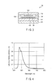
- FIG. 3 is a cross-sectional view showing a lighting device according to an embodiment.
- a lighting device 100 has a structure in which an anode 107 , an organic light-emitting diode layer 106 and a cathode 105 are formed in this order on a glass substrate 101 .
- a seal glass 102 is disposed so as to cover the cathode 105 and adhered using a UV adhesive 104 .
- a drying agent 103 is disposed on the cathode 105 side of the seal glass 102 .
- PVDBT was used as a host material of an emitting layer to fabricate an organic light-emitting diode.
- the layer structure of this diode is as follows: ITO 100 nm/PEDOT:PSS 50 nm/PVDBT:FIrpic 70 nm/3TPYMB 10 nm/CsF 0.5 nm/Al 150 nm.
- the anode was a transparent electrode made of ITO (indium-tin oxide) 100 nm in thickness.
- an aqueous poly(ethylenedioxythiophene):poly(styrene.sulfonic acid)[PEDOT:PSS] solution which is conductive ink was used.
- An aqueous PEDOT:PSS solution was applied by spin coating, and dried under heating to form a hole-transport layer 50 nm in thickness.
- FIrpic bis(3,5-difluoro-2-(2-pyridyl)phenyl-(2-carboxypyridyl)iridium(III)
- FIrpic polyvinyldibenzothiophene (number average molecular weight: 50,000, molecular weight distribution: 3.2) was used as the host material.
- the electron-transport layer was formed in a thickness of 10 nm by vapor evaporation of tris[3-(3-pyridyl)-mesityl]borane [3TPYMB].
- the electron injection layer was formed of CsF 0.5 nm in thickness and the cathode was formed of Al 150 nm in thickness.
- An organic light-emitting diode was prepared in a manner similar to Example 1, except that PVK was used as a host material for comparison.
- PVK Poly(9-vinylcarbazole) (trade name, manufactured by Aldrich, Catalog No. 368350, molecular weight distribution (polymerization degree): 2, number average molecular weight: 25,000 to 50,000) was used as PVK.
- the electroluminescence (EL) spectra at voltage application of the organic light-emitting diodes according to Example and Comparative Example were measured.
- the measurement was conducted by using a high sensitivity multi-channel spectroscope C10027-01 manufactured by Hamamatsu Photonics K.K.
- the results are shown in FIG. 4 .
- the spectra of Example and Comparative Example were completely overlapped, and thus it could be confirmed that the emitting dopant emitted blue light in both of the organic light-emitting diodes. It was found from this result that PVDBT used in Example is useful as a host material for organic light-emitting diodes.
- the luminous efficiency was obtained by measuring a luminance and measuring a current and a voltage at the same time.
- the luminance was measured using a Si Photodiode S7610 (trade name, manufactured by Hamamatsu Photonics K.K.) with a visibility filter.
- the current and the voltage were measured using a Semiconductor Parameter Analyzer 4156b (trade name, manufactured by Hewlett Packard). The results are shown in FIG. 5 .
- the lifetimes of the diodes were compared.
- the lifetime of the diode was evaluated by measuring the luminance over time. The luminance was measured using a Si Photodiode S7610 (trade name, manufactured by Hamamatsu Photonics K.K.) with a visibility filter.
- the results are shown in FIG. 6 .
- the standardized luminance on the vertical axis means, when the luminance at time 0 is defined as 1, a luminance at each time thereafter that is represented by a ratio with respect to the luminance at time 0. Namely, the standardized luminance can be represented by the formula: the actually measured luminance at each time/the luminance at time 0. It is found from FIG. 6 that the lifetime of the organic light-emitting diode of Example is about 2.8 times of that of the organic light-emitting diode of Comparative Example. From this result, it can be considered that PVDBT is hardly deteriorated by passage of an electrical charge, and a diode having a long lifetime can be obtained by using it as a host material for an organic light-emitting diode.
- an organic light-emitting diode having improved lifetime and luminance, and a display and a lighting device using the diode can be provided.
Landscapes
- Chemical & Material Sciences (AREA)
- Engineering & Computer Science (AREA)
- Materials Engineering (AREA)
- Electroluminescent Light Sources (AREA)
- Devices For Indicating Variable Information By Combining Individual Elements (AREA)
Applications Claiming Priority (2)
| Application Number | Priority Date | Filing Date | Title |
|---|---|---|---|
| JP2011-050622 | 2011-03-08 | ||
| JP2011050622A JP5330429B2 (ja) | 2011-03-08 | 2011-03-08 | 有機電界発光素子、表示装置および照明装置 |
Publications (2)
| Publication Number | Publication Date |
|---|---|
| US20120228585A1 US20120228585A1 (en) | 2012-09-13 |
| US8580403B2 true US8580403B2 (en) | 2013-11-12 |
Family
ID=44584078
Family Applications (1)
| Application Number | Title | Priority Date | Filing Date |
|---|---|---|---|
| US13/224,906 Active 2031-12-15 US8580403B2 (en) | 2011-03-08 | 2011-09-02 | Organic light-emitting diode, display and illuminating device |
Country Status (5)
| Country | Link |
|---|---|
| US (1) | US8580403B2 (ja) |
| EP (1) | EP2498314A1 (ja) |
| JP (1) | JP5330429B2 (ja) |
| CN (1) | CN102683614B (ja) |
| TW (1) | TW201237138A (ja) |
Cited By (2)
| Publication number | Priority date | Publication date | Assignee | Title |
|---|---|---|---|---|
| US9214642B2 (en) | 2013-07-04 | 2015-12-15 | Boe Technology Group Co., Ltd. | OLED device and manufacturing method thereof, display apparatus |
| US9773980B2 (en) | 2013-04-05 | 2017-09-26 | Kabushiki Kaisha Toshiba | Organic electroluminescent device |
Families Citing this family (2)
| Publication number | Priority date | Publication date | Assignee | Title |
|---|---|---|---|---|
| CN104037361B (zh) * | 2014-06-25 | 2016-06-15 | 上海道亦化工科技有限公司 | 一种有机电致发光器件 |
| CN104916790B (zh) * | 2015-03-05 | 2017-05-03 | 上海道亦化工科技有限公司 | 一种有机电致发光器件 |
Citations (9)
| Publication number | Priority date | Publication date | Assignee | Title |
|---|---|---|---|---|
| US2499187A (en) | 1948-06-17 | 1950-02-28 | Gen Electric | Polymers of 2-vinyldibenzothiophene |
| JP2001160490A (ja) | 1999-12-06 | 2001-06-12 | Taiho Ind Co Ltd | 有機エレクトロルミネッセンス素子及びその製造方法 |
| JP2002299059A (ja) | 2001-03-29 | 2002-10-11 | Ricoh Co Ltd | 光書込み用有機電界発光素子およびその製造方法 |
| WO2008029729A1 (fr) | 2006-09-08 | 2008-03-13 | Konica Minolta Holdings, Inc. | Dispositif électroluminescent organique, dispositif d'éclairage et affichage utilisant un tel dispositif |
| JP2008074939A (ja) | 2006-09-21 | 2008-04-03 | Konica Minolta Holdings Inc | 有機エレクトロルミネッセンス素子材料、有機エレクトロルミネッセンス素子、表示装置及び照明装置 |
| US20090017331A1 (en) * | 2007-07-10 | 2009-01-15 | Idemitsu Kosan Co., Ltd. | Material for organic electroluminescence device and organic electroluminescence device utilizing the same |
| WO2009147011A1 (en) | 2008-06-02 | 2009-12-10 | Basf Se | Dibenzofurane polymers for electroluminiscent devices |
| WO2010079051A1 (de) | 2009-01-07 | 2010-07-15 | Basf Se | Silyl- und heteroatom-substituierte verbindungen ausgewählt aus carbazolen, dibenzofuranen, dibenzothiophenen und dibenzophospholen und ihre anwendung in der organischen elektronik |
| WO2010122810A1 (ja) | 2009-04-24 | 2010-10-28 | 出光興産株式会社 | 芳香族アミン誘導体及びそれを用いた有機エレクトロルミネッセンス素子 |
Family Cites Families (3)
| Publication number | Priority date | Publication date | Assignee | Title |
|---|---|---|---|---|
| JP5157442B2 (ja) * | 2005-04-18 | 2013-03-06 | コニカミノルタホールディングス株式会社 | 有機エレクトロルミネッセンス素子、表示装置及び照明装置 |
| WO2009119163A1 (ja) * | 2008-03-24 | 2009-10-01 | 新日鐵化学株式会社 | 有機電界発光素子用化合物及びこれを用いた有機電界発光素子 |
| JP5329342B2 (ja) * | 2008-09-01 | 2013-10-30 | 株式会社半導体エネルギー研究所 | 発光素子 |
-
2011
- 2011-03-08 JP JP2011050622A patent/JP5330429B2/ja active Active
- 2011-09-01 CN CN201110309207.3A patent/CN102683614B/zh not_active Expired - Fee Related
- 2011-09-01 TW TW100131470A patent/TW201237138A/zh unknown
- 2011-09-02 US US13/224,906 patent/US8580403B2/en active Active
- 2011-09-05 EP EP11180008A patent/EP2498314A1/en not_active Withdrawn
Patent Citations (9)
| Publication number | Priority date | Publication date | Assignee | Title |
|---|---|---|---|---|
| US2499187A (en) | 1948-06-17 | 1950-02-28 | Gen Electric | Polymers of 2-vinyldibenzothiophene |
| JP2001160490A (ja) | 1999-12-06 | 2001-06-12 | Taiho Ind Co Ltd | 有機エレクトロルミネッセンス素子及びその製造方法 |
| JP2002299059A (ja) | 2001-03-29 | 2002-10-11 | Ricoh Co Ltd | 光書込み用有機電界発光素子およびその製造方法 |
| WO2008029729A1 (fr) | 2006-09-08 | 2008-03-13 | Konica Minolta Holdings, Inc. | Dispositif électroluminescent organique, dispositif d'éclairage et affichage utilisant un tel dispositif |
| JP2008074939A (ja) | 2006-09-21 | 2008-04-03 | Konica Minolta Holdings Inc | 有機エレクトロルミネッセンス素子材料、有機エレクトロルミネッセンス素子、表示装置及び照明装置 |
| US20090017331A1 (en) * | 2007-07-10 | 2009-01-15 | Idemitsu Kosan Co., Ltd. | Material for organic electroluminescence device and organic electroluminescence device utilizing the same |
| WO2009147011A1 (en) | 2008-06-02 | 2009-12-10 | Basf Se | Dibenzofurane polymers for electroluminiscent devices |
| WO2010079051A1 (de) | 2009-01-07 | 2010-07-15 | Basf Se | Silyl- und heteroatom-substituierte verbindungen ausgewählt aus carbazolen, dibenzofuranen, dibenzothiophenen und dibenzophospholen und ihre anwendung in der organischen elektronik |
| WO2010122810A1 (ja) | 2009-04-24 | 2010-10-28 | 出光興産株式会社 | 芳香族アミン誘導体及びそれを用いた有機エレクトロルミネッセンス素子 |
Non-Patent Citations (5)
| Title |
|---|
| Extended European Search Report for European Application No. 11180008.2 dated Jun. 14, 2012. |
| Japanese First Office Action for Application No. 2011-050622 Dated Jan. 8, 2013, 5 pages. |
| M.-J. Yang, et al., "Use of Poly (9-vinylcarbazole) as Host Material for Iridium Complexes in High-Efficiency Organic Light-Emitting Devices", Jpn. J. Appl Phys., vol. 39, 2000, pp. L828-L829. |
| Shimomura, Osamu, et al., "Synthesis and Radical Polymerization of 2-Vinyldibenzothiophene", Journal of Polymer Science: Part A: Polymer Chemistry, 1997, vol. 35, 281-2819. |
| Shimomura, Osamu, et al., "Synthesis and Radical Polymerization of 2-Vinyldibenzothiophene", Journal of Polymer Science: Part A: Polymer Chemistry, 1997, vol. 35, 2813-2819. |
Cited By (2)
| Publication number | Priority date | Publication date | Assignee | Title |
|---|---|---|---|---|
| US9773980B2 (en) | 2013-04-05 | 2017-09-26 | Kabushiki Kaisha Toshiba | Organic electroluminescent device |
| US9214642B2 (en) | 2013-07-04 | 2015-12-15 | Boe Technology Group Co., Ltd. | OLED device and manufacturing method thereof, display apparatus |
Also Published As
| Publication number | Publication date |
|---|---|
| EP2498314A1 (en) | 2012-09-12 |
| TW201237138A (en) | 2012-09-16 |
| US20120228585A1 (en) | 2012-09-13 |
| JP2012190843A (ja) | 2012-10-04 |
| CN102683614A (zh) | 2012-09-19 |
| CN102683614B (zh) | 2015-04-15 |
| JP5330429B2 (ja) | 2013-10-30 |
Similar Documents
| Publication | Publication Date | Title |
|---|---|---|
| CN102694127B (zh) | 有机电场发光元件、显示装置和照明装置 | |
| CN102683615B (zh) | 有机电致发光元件、显示装置和照明装置 | |
| JP5487174B2 (ja) | 有機電界発光素子、表示装置および照明装置 | |
| US8679646B2 (en) | Organic light-emitting diode, display and illuminating device | |
| US20120056162A1 (en) | Novel compound and organic light-emitting diode, display and illuminating device using the same | |
| CN101535445A (zh) | 光发射器件 | |
| US20110175067A1 (en) | Organic light-emitting diode | |
| US8580403B2 (en) | Organic light-emitting diode, display and illuminating device | |
| CN102742354A (zh) | 有机电致发光元件、其制造方法及制造装置 | |
| US9136485B2 (en) | Compound and organic light-emitting diode, display and illuminating device using the compound | |
| US8535815B2 (en) | Compound and organic light-emitting diode, display and lighting device using the same | |
| US20120181515A1 (en) | Organic light-emitting diode, display and illuminating device | |
| US9666823B2 (en) | Organic electroluminescent element and method for manufacturing the same | |
| JP5178794B2 (ja) | 新規化合物ならびにそれを使用した有機電界発光素子、表示装置および照明装置 | |
| JP2014532983A (ja) | 照明用有機電子デバイス | |
| US8835916B2 (en) | Organic thin film and organic electroluminescent element containing same in light-emitting layer | |
| Fehse et al. | Highly efficient OLEDs on ITO-free polymeric substrates | |
| US9705100B2 (en) | Organic electroluminescent element and method for manufacturing the same | |
| WO2011030408A1 (ja) | 有機電界発光素子 |
Legal Events
| Date | Code | Title | Description |
|---|---|---|---|
| AS | Assignment |
Owner name: KABUSHIKI KAISHA TOSHIBA, JAPAN Free format text: ASSIGNMENT OF ASSIGNORS INTEREST;ASSIGNORS:MIZUNO, YUKITAMI;AMEMIYA, ISAO;HIRAO, AKIKO;AND OTHERS;SIGNING DATES FROM 20110912 TO 20110915;REEL/FRAME:027107/0389 |
|
| STCF | Information on status: patent grant |
Free format text: PATENTED CASE |
|
| FEPP | Fee payment procedure |
Free format text: PAYOR NUMBER ASSIGNED (ORIGINAL EVENT CODE: ASPN); ENTITY STATUS OF PATENT OWNER: LARGE ENTITY |
|
| FPAY | Fee payment |
Year of fee payment: 4 |
|
| MAFP | Maintenance fee payment |
Free format text: PAYMENT OF MAINTENANCE FEE, 8TH YEAR, LARGE ENTITY (ORIGINAL EVENT CODE: M1552); ENTITY STATUS OF PATENT OWNER: LARGE ENTITY Year of fee payment: 8 |
|
| MAFP | Maintenance fee payment |
Free format text: PAYMENT OF MAINTENANCE FEE, 12TH YEAR, LARGE ENTITY (ORIGINAL EVENT CODE: M1553); ENTITY STATUS OF PATENT OWNER: LARGE ENTITY Year of fee payment: 12 |