US8570668B2 - Imaging optical system and imaging apparatus - Google Patents
Imaging optical system and imaging apparatus Download PDFInfo
- Publication number
- US8570668B2 US8570668B2 US13/237,238 US201113237238A US8570668B2 US 8570668 B2 US8570668 B2 US 8570668B2 US 201113237238 A US201113237238 A US 201113237238A US 8570668 B2 US8570668 B2 US 8570668B2
- Authority
- US
- United States
- Prior art keywords
- side prism
- image side
- optical system
- image
- imaging
- Prior art date
- Legal status (The legal status is an assumption and is not a legal conclusion. Google has not performed a legal analysis and makes no representation as to the accuracy of the status listed.)
- Expired - Fee Related, expires
Links
Images


Classifications
-
- G—PHYSICS
- G02—OPTICS
- G02B—OPTICAL ELEMENTS, SYSTEMS OR APPARATUS
- G02B13/00—Optical objectives specially designed for the purposes specified below
- G02B13/001—Miniaturised objectives for electronic devices, e.g. portable telephones, webcams, PDAs, small digital cameras
- G02B13/0055—Miniaturised objectives for electronic devices, e.g. portable telephones, webcams, PDAs, small digital cameras employing a special optical element
- G02B13/0065—Miniaturised objectives for electronic devices, e.g. portable telephones, webcams, PDAs, small digital cameras employing a special optical element having a beam-folding prism or mirror
Definitions
- the present invention relates to an imaging optical system, and an imaging apparatus having the imaging optical system.
- Such cameras and digital electronic devices include a device in which an imaging optical system (a so-called bending optical system) configured to have an optical path elongated in a direction orthogonal to a direction of thickness of a device body is mounted so as to decrease the thickness of the device body.
- an imaging optical system a so-called bending optical system
- the direction of thickness of a device body is referred to as “a case thickness direction”
- the direction orthogonal to the case thickness direction is referred to as “a case surface direction”.
- a sensor surface of an image pickup chip needs to be positioned to be parallel with the case thickness direction so that an object image can be incident on the sensor surface of the image pickup chip.
- an outer dimension of the image pickup chip in the sensor surface direction is large, it becomes difficult to design a device body case to be thin when the sensor surface is positioned to be parallel with the case thickness direction.
- Each of Japanese Patent Provisional Publications No. 2006-058840A, No. 2006-154702A, No. 2007-033819A, No. 2004-247887A, No. 2007-316528A and No. 2008-268700A discloses an imaging optical system configured to decrease the dimension in the case thickness direction by positioning a sensor surface of an image pickup chip to be parallel with the case surface direction. Specifically, in the imaging optical system disclosed in these publications, a prism is arranged immediately before the image pickup chip and an optical path is bent to the case thickness direction.
- the prism is located immediately before the image pickup chip. Therefore, unwanted light not contributing to normal image formation is caused, and the unwanted light appears on an image as a ghost or flare.
- the ghost or flare may result in an unintended image or decreasing of the contrast. That is, the ghost or flare deteriorates the image quality.
- As effective measures for suppressing occurrence of a ghost or flare one might consider arranging a shield mask on an optical path between an optical element causing the unwanted light and the image pickup chip.
- it might be impossible to sufficiently suppress the unwanted light by only arranging the shield mask and therefore it might become impossible to avoid deterioration of the quality of an image even when the shield mask is arranged.
- the present invention is advantageous in that it provides an imaging optical system and an imaging apparatus capable of decreasing the thickness of the imaging apparatus while preventing occurrence of unwanted light by a prism located immediately before an image pickup chip.
- an imaging optical system which includes an imaging lens group having at least one lens, and an image side prism that bends light which has passed through the imaging lens group toward an image pickup device arranged at a predetermined position.
- the image side prism includes a reflection surface which reflects, toward the image pickup device, incident light proceeding from the imaging lens group, and an exit surface from which light reflected from the reflection surface emerges.
- the image side prism has a cut surface formed by cutting off a vertex portion between the reflection surface and the exit surface such that a whole normal light incident area within which normal light is incident on the reflection surface remains. The cut surface is a non-diffusing surface.
- the imaging optical system is configured as a so-called bending optical system which is advantageous in designing an imaging apparatus to be thin. That is, it is possible to provide an imaging apparatus capable of decreasing the thickness thereof while preventing occurrence of unwanted light by a prism located immediately before an image pickup device.
- the imaging optical system may satisfy a condition: ⁇ > ⁇ /2 ⁇ SIN ⁇ 1 ( No/Np ) (1).
- the imaging optical system may satisfy a condition: ⁇ >( ⁇ /2+SIN ⁇ 1 ( No/Np ))/2 (2).
- the image side prism may bend an optical path by approximately 90°.
- the imaging optical system may further include an object side prism located on an object side with respect to the image side prism.
- the object side prism is arranged such that at least one lens of lenses of the imaging lens group is located between the object side prism and the image side prism.
- the object side prism bends an optical path by approximately 90°.
- an imaging apparatus which includes one of the above described imaging optical systems, and an image pickup device.
- the image pickup device is arranged such that a sensor surface of the image pickup device is positioned on an image plane of the imaging optical system.
- FIGS. 1A and 1B illustrate a configuration of an imaging apparatus according to an embodiment of the invention.
- FIG. 2 is an explanatory illustration for explaining an example of a ghost or flare caused by unwanted light in a conventional imaging optical system.
- FIGS. 3A , 3 B and 3 C are explanatory illustrations for explaining an optical path of a light ray which has entered an image side prism according to the embodiment of the invention.
- FIG. 4 illustrates a configuration of the imaging optical system according to a first example of the invention.
- FIG. 5 illustrates a configuration of the imaging optical system according to a second example of the invention.
- FIG. 6 illustrates a configuration of the imaging optical system according to a third example of the invention.
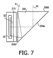
- FIG. 7 illustrates a configuration of an imaging optical system according to a first comparative example.
- FIG. 8 illustrates a configuration of the imaging optical system according to a second comparative example.
- FIG. 9 illustrates a configuration of the imaging optical system according to a third comparative example.
- FIG. 10 is an explanatory illustration for explaining the dimension of the image side prism of each of the first to third examples and the image side prism of each of the first to third comparative examples.
- FIGS. 1A and 1B illustrate a configuration of an imaging apparatus 1 according to the embodiment of the invention.
- an optical configuration of the imaging apparatus 1 i.e., a substantial part of the embodiment
- a mechanical configuration and a circuit configuration which are not substantial parts of the embodiment are omitted for the sake of simplicity.
- the imaging apparatus 1 is, for example, a mobile phone.
- the imaging apparatus 1 may be a digital camera, a digital video camera or a digital electronic device in which an imaging module is mounted, such as a mobile phone, PDA, PND, PHS, a portable game machine and a notebook computer.
- the imaging apparatus 1 may be an imaging module.
- the imaging apparatus 1 includes a case 10 having a thickness T.
- the direction of the thickness T of the case 10 is defined as a Z axis direction, and two directions which are perpendicular to the Z axis direction and are perpendicular to each other are defined as a X axis direction (perpendicular to a paper face of FIGS. 1A and 1B ) and a Y axis direction (parallel with the paper face of FIGS. 1A and 1B ).
- An internal block diagram of a box indicated by a dashed line in FIG. 1A is illustrated in FIG. 1B . As shown in FIG.
- the imaging apparatus 1 includes an imaging optical system 100 .
- the imaging optical system 100 includes an objective lens 102 , an object side prism 104 , an imaging lens group 106 , an image side prism 108 and a cover glass 110 .
- Each of the object side prism 104 and the image side prism 108 is a right angle prism configured to bend an optical path by 90°.
- an aperture stop S is arranged in the imaging lens group 106 .
- a chain line represents an optical axis AX of the imaging optical system 100 .
- the objective lens 102 Light proceeding in the Z axis direction (i.e., the case thickness direction) from an object is incident on the objective lens 102 and is bent toward the Y axis direction (i.e., the case surface direction) by the object side prism 104 . Then, the light passes through the imaging lens group 106 , and is bent again toward the Z axis direction by a reflection surface 108 a of the image side prism 108 . The light which has reflected from the reflection surface 108 a passes through an exit surface 108 b of the image side prism 108 , and passes through the cover glass 110 .
- the cover glass 110 seals an image pickup chip 20 adhered to a resin package.
- the light which has passed through the cover glass 100 is incident, within an effective pixel area of a sensor surface 22 , on the sensor surface 22 of the image pickup chip 20 .
- the image pickup chip 20 is arranged such that the sensor surface 22 is parallel with the XY plane so as to let the light bent toward the Z axis direction by the reflection surface 108 a be perpendicularly incident on the affective pixel area of the sensor surface 22 .
- the image pickup chip 20 is, for example, a single-chip color CMOS (Complementary Metal Oxide Semiconductor) image sensor having a bayer layout.
- the sensor surface 22 of the image pickup chip 20 is located on an image plane of the imaging lens group 106 .
- the image pickup chip 20 accumulates, at each pixel, charges responsive to a light amount of an optical image formed on the sensor surface 22 , and converts the charges into an image signal.
- the image signal is input to an image processing engine (not shown).
- the image processing engine executes various types of image processing, such as, generating an image by processing the image signal, displaying the generated image and recording the generated image in a recording medium.
- the image pickup chip 20 is not limited to the CMOS sensor chip, and various types of image pickup chips (e.g., a CCD (Charge Couple Device) image sensor chip) may be used as the image pickup chip 20 .
- CCD Charge Couple Device
- FIG. 2 is an explanatory illustration for explaining an example of a ghost or flare caused by unwanted light in a conventional imaging optical system 200 .
- a light ray R is on the outside of the maximum field angle (hereafter, light on the outside of the maximum field angle is simply referred to as “light outside the field angle”), and, according to a design condition, the light ray R is not incident on the effective pixel area of the sensor surface 22 .
- FIG. 2 showing the conventional imaging optical system 200 , to elements which are substantially the same as those of the embodiment, the same reference numbers are assigned and explanations thereof will not be repeated.
- the conventional imaging optical system 200 shown in FIG. 2 includes an objective lens 202 , an object side prism 204 , an imaging lens group 206 , an image side prism 208 and a cover glass 210 .
- the light ray R is incident on the objective lens 202 and is bent by the object side prism 204 by 90°. Then, the light ray R is incident on the image side prism 208 after passing through the imaging lens group 206 .
- the light ray R is incident on an exit surface 208 b of the image side prism 208 .
- An incident angle of the light ray R with respect to the exit surface 208 b is large, and is larger than or equal to a critical angle. Therefore, the light ray R totally reflects from the exit surface 208 b .
- the light ray R which has totally reflected from the exit surface 208 b is incident on a reflection surface 208 a of the image side prism 208 . Then, the light ray R passes through the exit surface 208 b after totally reflecting again from the reflection surface 208 a . Then, the light ray R passes through the cover glass 210 , and is incident on the sensor surface 22 within an effective pixel area of the sensor surface 22 .
- the light outside the field angle which has totally reflected from the exit surface 208 b appears on an image as a ghost or flare, and thereby deteriorates the quality of the image.
- a vertex portion formed between the reflection surface 108 a and the exit surface 108 b of the image side prism 108 is cut off in order to suppress occurrence of a ghost or flare of the above described type.
- a cut surface 108 c is formed.
- the vertex portion is cut off such that a normal light incident area on the reflection surface 108 a remains (i.e., the normal light incident area is not cut off).
- the normal light incident area means an area within which the normal light falls (i.e., an area indicated by an arrow F in FIG. 10 ).
- an angle formed between the cut surface 108 c i.e., a connection surface which connects the reflection surface 108 a with the exit surface 108 b
- the exit surface 108 b is larger than an angle formed between the reflection surface 108 a and the exit surface 108 b.
- FIG. 3A is an explanatory illustration for explaining an optical path of the light ray R which has entered the image side prism 108 .
- the light ray R which has entered the image side prism 108 totally reflects from the exit surface 108 b , and then is incident on the cut surface 108 c . Since the angle formed between the cut surface 108 c and the exit surface 108 b is larger than the angle formed between the exit surface 108 b and the reflection surface 108 a , the incident angle of the light ray R with respect to the cut surface 108 c is smaller than the incident angle of the light ray R in the case of FIG.
- a reflection component of the light ray R reflecting from the cut surface 108 c decreases in comparison with the case shown in FIG. 2 (i.e., a reflection component of the light ray R reflecting from the reflections surface 208 a ). Thanks to the decrease of the reflecting component, the light outside the field angle which has totally reflected from the exit surface 108 b becomes hard to appear in the image as a ghost or flare.
- the incident angle of the light ray R with respect to the cut surface 108 c is smaller than the critical angle. Therefore, the light ray R passes through the cut surface 108 c .
- the light which has passes through the reflection surface 108 a propagates to the outside of the effective pixel area of the sensor surface 22 . Therefore, according to the embodiment, occurrence of a ghost or flare can be suppressed effectively.
- the reflection component i.e., light reflected from the cut surface 108 c
- the reflection surface 108 a after totally reflecting from the exit surface 108 b and an entrance surface 108 d in this order. Since the light which has passed through the reflection surface 108 a propagates to the outside of the effective pixel area of the sensor surface 22 , occurrence of a ghost or flare can be suppressed effectively.
- the imaging optical system 100 may be configured to satisfy a following condition (1). ⁇ > ⁇ /2 ⁇ SIN ⁇ 1 ( No/Np ) (1)
- FIG. 3B is an explanatory illustration for explaining derivation of the condition (1).
- the incident angle of the light ray R with respect to the exit surface 108 b is defined as ⁇ 1
- the incident angle of the light ray R with respect to the cut surface 108 c is defined as ⁇ 2 .
- ⁇ 2 ⁇ 1 ⁇ in FIG. 3B
- ⁇ 2 ⁇ can be rewritten into: ⁇ 1 ⁇ SIN ⁇ 1 ( No/Np )
- the above indicated expression can be rewritten into: ⁇ > ⁇ 1 ⁇ SIN ⁇ 1 ( No/Np ) Since the maximum value of ⁇ 1 is 90 degrees, the condition (1) can be derived from the above indicated expression.
- the imaging optical system 100 may be configured to satisfy a following condition (2). ⁇ >( ⁇ /2+SIN ⁇ 1 ( No/Np ))/2 (2)
- the reflection component i.e., the light reflected from the cut surface 108 c
- the condition (2) is satisfied, the reflection component (i.e., the light reflected from the cut surface 108 c ) totally reflects from the exit surface 108 b . Therefore, occurrence of a ghost or flare can be suppressed more effectively.
- the condition (2) is not satisfied, a possibility arises that the reflection component of light from the cut surface 108 c impinges on the effective pixel area of the sensor surface 22 after passing through the exit surface 108 b . In this case, a ghost or flare becomes easy to occur.
- FIG. 3C is an explanatory illustration for explaining derivation of the condition (2).
- the angles ⁇ 1 and ⁇ 2 are defined in FIG. 3C .
- an incident angle of the reflection component of light from the cut surface 108 c with respect to the exit surface 108 b is defined as ⁇ 3 .
- the incident angle ⁇ 3 is larger than the critical angle ⁇ , the light ray R totally reflects from the exit surface 108 b.
- the imaging optical system 100 according to each of the first to third examples has a common configuration on the object side with respect to the image side prism 108 as shown in FIG. 1 . Therefore, in the following explanation for the first to third examples, only the optical configuration after the image side prism 108 is explained for the sake of simplicity.
- the first to third comparative examples according to the conventional imaging optical system 200 have a common configuration on the object side with respect to the image side prism 208 as shown in FIG. 2 .
- FIG. 4 illustrates a configuration of the imaging optical system 100 according to the first example.
- Table 1 shows a numeric configuration (design values) of the imaging optical system 100 according to the first example.
- R denotes the curvature radius (unit: mm) of each optical surface
- D denotes the thickness of an optical component or the distance (unit: mm) from each optical surface to the next optical surface on the optical axis AX
- Nd represents the refractive index at a d-line (the wavelength of 588 nm).
- Table and drawings of the first example are also applied to the following examples and the comparative examples.
- each of the imaging optical systems 100 and 200 has the focal length of 4.0 mm, and the maximum image height in a cross sectional plane (YZ plane) in which the optical path is bent by the image side prism ( 108 or 208 ) is 2.45 mm.
- FIG. 5 illustrates a configuration of the imaging optical system 100 according to the second example.
- Table 2 shows a numeric configuration (design values) of the imaging optical system 100 according to the second example.
- surfaces # 1 to # 10 have the same numeric values as those of the surfaces # 1 to # 10 in Table 1, and therefore explanations thereof will not be repeated for the sake of simplicity.
- FIG. 6 illustrates a configuration of the imaging optical system 100 according to the third example.
- Table 3 shows a numeric configuration (design values) of the imaging optical system 100 according to the third example.
- FIG. 7 illustrates a configuration of the imaging optical system 200 according to the first comparative example
- FIG. 8 illustrates a configuration of the imaging optical system 200 according to the second comparative example
- FIG. 9 illustrates a configuration of the imaging optical system 200 according to the third comparative example.
- the numeric configurations of the first to third comparative examples are respectively equal to those of the above described first to third examples (the imaging optical system 100 ), excepting that each of the first to third comparative examples does not have the cut surface 108 c.
- FIG. 10 is an explanatory illustration for explaining the dimension of the image side prism 108 of each of the first to third examples and the image side prism 208 of each of the first to third comparative examples.
- a dashed line represents the optical path of the normal light.
- the field angle of the normal light is ⁇ 20.2°.
- Table 4 shows the dimensions of the image side prism 108 of each of the first to third examples and the image side prism 208 of each of the first to third comparative examples. In Table 4, the dimensions corresponding to reference symbols used in FIG. 10 are shown. In Table 4, the unit of each dimension is mm.
- Table 5 shows values of the angle ⁇ , the right term of the condition (1), the right term of the condition (2) and the incident angle of the light ray R with respect to the entrance surface 108 d of each of the first to third examples and the first to third comparative examples. Since each of the first to third comparative examples does not have the cut surface 108 c , the angle between the reflection surface 208 a and the exit surface 208 b is represented as a for convenience of illustration.
- the image side prism 208 of each of the first to third comparative examples does not have the cut surface 108 c , the light outside the field angle which has totally reflected from the exit surface 208 b tends to totally reflect from the reflection surface 208 a and thereby to enter the effective pixel area of the sensor surface 22 . That is, in the imaging optical system 200 according to each of the first to third comparative examples, the light outside the field angle which has totally reflected from the exit surface 208 b tends to appear on an image as a ghost or flare.
- the image side prism 108 according to each of the first to third examples has the cut surface 108 c . Therefore, the light outside the field angle which has totally reflected from the exit surface 108 b passes through the cut surface 108 c and propagates to the outside of the effective pixel area of the sensor surface 22 . That is, the light outside the field angle which has totally reflected from the exit surface 108 b is hard to appear on an image as a ghost or flare. Since the imaging optical system according to each of the first to third examples satisfies the condition (1), total reflection does not occur on the cut surface 108 c .
- the light totally reflected from the exit surface 108 b passes through the cut surface 108 c and propagates to the outside of the effective pixel area of the sensor surface 22 . Therefore, occurrence of a ghost or flare can be suppressed more effectively. Since the imaging optical system 100 according to each of the first to third examples satisfies also the condition (2), the reflection component of light from the cut surface 10 c totally reflects from the exit surface 108 b , and therefore does not enter the sensor surface 22 . Therefore, occurrence of a ghost or flare can be suppressed more effectively.
- the object side prism 104 may be substituted by a mirror serving to bend an optical path.
- the object side prism 104 may not be arranged at the position on the object side with respect to the imaging lens group 106 .
- the object side prism 104 may be arranged at a position between lenses constituting the imaging lens group 106 .
- the cut surface 108 c is formed as a light-transmitting surface.
- the cut surface 108 c may be formed as a light absorption surface.
- the light absorption surface is, for example, a surface which is formed by applying, to a ground optical surface, coating material which has a refractive index close to the medium (i.e., the image side prism 108 ) and has a light absorption structure (e.g., black ink). If the cut surface 108 c close to the sensor surface 22 is formed as a diffusing surface, the diffused light might enter the sensor surface 22 and thereby appears on an image as a ghost or flare. Therefore, it is not desirable to form the cut surface 108 c as a diffusing surface.
Landscapes
- Physics & Mathematics (AREA)
- General Physics & Mathematics (AREA)
- Optics & Photonics (AREA)
- Lenses (AREA)
- Studio Devices (AREA)
- Optical Elements Other Than Lenses (AREA)
- Structure And Mechanism Of Cameras (AREA)
Abstract
Description
α>π/2−SIN−1(No/Np) (1).
α>(π/2+SIN−1(No/Np))/2 (2).
α>π/2−SIN−1(No/Np) (1)
θ1−α<SIN−1(No/Np)
Furthermore, the above indicated expression can be rewritten into:
α>θ1−SIN−1(No/Np)
Since the maximum value of θ1 is 90 degrees, the condition (1) can be derived from the above indicated expression.
α>(π/2+SIN−1(No/Np))/2 (2)
When the condition (2) is satisfied, the reflection component (i.e., the light reflected from the
θ3=θ1−2θ2 and
θ2=θ1−α,
θ3=2α−θ1 can be derived.
θ3>θ can be rewritten into:
2α−θ1>SIN−1(No/Np)
α>(θ1+SIN−1(No/Np))/2
Since the maximum value of θ1 is 90 degrees, the condition (2) can be derived from the above indicated expression.
| TABLE 1 | |||||
| Surface No. | R | | Nd | Comments | |
| 1 | −38.947 | 0.700 | 1.58913 | |
| 2 | 3.451 | 1.030 | 1.00000 | |
| 3 | ∞ | 2.100 | 1.74400 | |
| 4 | ∞ | 2.100 | ||
| 5 | ∞ | 1.649 | 1.00000 | |
| 6 | 9.010 | 1.193 | 1.84666 | |
| 7 | −26.650 | 0.894 | 1.00000 | |
| 8 | ∞ | 1.167 | ||
| (aperture stop) | ||||
| 9 | 10.422 | 0.700 | 1.84666 | |
| 10 | 2.221 | 2.123 | 1.77250 | |
| 11 | −12.176 | 2.674 | 1.00000 | |
| 12 | ∞ | 2.500 | 1.74400 | |
| 13 | ∞ | 2.500 | ||
| 14 | ∞ | 0.200 | 1.00000 | |
| 15 | ∞ | 0.500 | 1.51633 | |
| 16 | ∞ | 0.300 | 1.00000 | |
| 17 | ∞ | |
||
| TABLE 2 | ||||
| Surface No. | R | D | Nd | Comments |
| 11 | −12.176 | 2.540 | 1.00000 | |
| 12 | ∞ | 2.500 | 1.69680 | |
| 13 | ∞ | 2.500 | ||
| 14 | ∞ | 0.200 | 1.00000 | |
| 15 | ∞ | 0.500 | 1.51633 | |
| 16 | ∞ | 0.380 | 1.00000 | |
| 17 | ∞ | |
||
| TABLE 3 | ||||
| Surface No. | R | D | Nd | Comments |
| 11 | −12.176 | 2.760 | 1.00000 | |
| 12 | ∞ | 2.500 | 1.83400 | |
| 13 | ∞ | 2.500 | ||
| 14 | ∞ | 0.200 | 1.00000 | |
| 15 | ∞ | 0.500 | 1.51633 | |
| 16 | ∞ | 0.380 | 1.00000 | |
| 17 | ∞ | |
||
| TABLE 4 | ||||
| | ||||
| Symbol | Comments | |||
| 1st Example | 2nd Example | 3rd Example | ||
| A | Width of |
5.00 | 5.00 | 5.00 |
| B | Width of |
5.89 | 5.83 | 5.99 |
| C | Width of |
0.95 | 0.99 | 0.87 |
| D | Width of |
4.60 | 4.56 | 4.65 |
| E | Distance Between Optical Axis AX | 2.50 | 2.50 | 2.50 |
| and |
||||
| F | Effective Area of Reflection Surface | 4.15 | 4.16 | 4.16 |
| 108a | ||||
| G | Distance between |
0.30 | 0.24 | 0.41 |
| and Effective Area of | ||||
| Surface | ||||
| 108a | ||||
| H | Distance Between Optical Axis AX | 2.50 | 2.50 | 2.50 |
| and |
||||
| I | Width of Effective Area of Sensor | 2.94 | 2.94 | 2.94 |
| |
||||
| 1st | 2nd | 3rd | ||
| comparative | comparative | comparative | ||
| Symbol | Comments | example | example | example |
| A | Width of |
5.00 | 5.00 | 5.00 |
| B | Width of |
7.07 | 7.07 | 7.07 |
| C | Width of |
— | — | — |
| D | Width of |
5.00 | 5.00 | 5.00 |
| E | Distance Between Optical Axis AX | 2.50 | 2.50 | 2.50 |
| and |
||||
| F | Effective Area of Reflection Surface | 4.15 | 4.16 | 4.16 |
| 208a | ||||
| G | Distance between |
— | — | — |
| and Effective Area of | ||||
| Surface | ||||
| 208a | ||||
| H | Distance Between Optical Axis AX | 2.50 | 2.50 | 2.50 |
| and |
||||
| I | Width of Effective Area of Sensor | 2.94 | 2.94 | 2.94 |
| |
||||
| TABLE 5 | ||||
| |
1st Example | 2nd Example | 3rd Example | |
| α | Degree | 62.6 | 63.2 | 61.6 |
| Right term of | Degree | 55.0 | 53.9 | 57.0 |
| condition (1) | ||||
| Right term of | Degree | 62.5 | 63.1 | 61.5 |
| condition (2) | ||||
| Incident angle of | Degree | 16.7 | 15.3 | 20.0 |
| light ray R with | ||||
| respect to | ||||
| surface | ||||
| 108d | ||||
| 1st | 2nd | 3rd | ||
| Comparative | Comparative | Comparative | ||
| Unit | Example | Example | Example | |
| α | Degree | 45.0 | 45.0 | 45.0 |
| Right term of | Degree | 55.0 | 53.9 | 57.0 |
| condition (1) | ||||
| Right term of | Degree | 62.5 | 63.1 | 61.5 |
| condition (2) | ||||
| Incident angle of | Degree | 16.7 | 15.3 | 20.0 |
| light ray R with | ||||
| respect to | ||||
| surface | ||||
| 208d | ||||
Claims (10)
α>π/2−SIN−1(N o /N p) (1).
α>(π/2+SIN−1(N o /N p))/2 (2).
α>π/2−SIN−1(N o /N p) (1).
α>(π/2+SIN−1(N o /N p))/2 (2).
Applications Claiming Priority (2)
| Application Number | Priority Date | Filing Date | Title |
|---|---|---|---|
| JP2010214153A JP2012068510A (en) | 2010-09-24 | 2010-09-24 | Photographic optical system and photographic device |
| JP2010-214153 | 2010-09-24 |
Publications (2)
| Publication Number | Publication Date |
|---|---|
| US20120075726A1 US20120075726A1 (en) | 2012-03-29 |
| US8570668B2 true US8570668B2 (en) | 2013-10-29 |
Family
ID=45870410
Family Applications (1)
| Application Number | Title | Priority Date | Filing Date |
|---|---|---|---|
| US13/237,238 Expired - Fee Related US8570668B2 (en) | 2010-09-24 | 2011-09-20 | Imaging optical system and imaging apparatus |
Country Status (2)
| Country | Link |
|---|---|
| US (1) | US8570668B2 (en) |
| JP (1) | JP2012068510A (en) |
Cited By (40)
| Publication number | Priority date | Publication date | Assignee | Title |
|---|---|---|---|---|
| US9465199B2 (en) | 2013-10-15 | 2016-10-11 | Hoya Corporation | Imaging optical system having bending optical element |
| US9560249B2 (en) | 2014-10-20 | 2017-01-31 | Hoya Corporation | Imaging apparatus having bending optical element |
| US20170131526A1 (en) * | 2015-11-09 | 2017-05-11 | Samsung Electronics Co., Ltd. | Reflecting imaging apparatus and mobile device having the same |
| EP3461284A4 (en) * | 2017-07-07 | 2019-07-03 | Corephotonics Ltd. | Folded camera prism design for preventing stray light |
| US10386605B2 (en) | 2016-07-14 | 2019-08-20 | Largan Precision Co., Ltd. | Optical photographing assembly, image capturing apparatus, and electronic device comprising five-lens system having inflection point |
| US10437020B2 (en) | 2013-07-04 | 2019-10-08 | Corephotonics Ltd. | Miniature telephoto lens assembly |
| US10509209B2 (en) | 2014-08-10 | 2019-12-17 | Corephotonics Ltd. | Zoom dual-aperture camera with folded lens |
| US10534153B2 (en) | 2017-02-23 | 2020-01-14 | Corephotonics Ltd. | Folded camera lens designs |
| US10620450B2 (en) | 2013-07-04 | 2020-04-14 | Corephotonics Ltd | Thin dual-aperture zoom digital camera |
| US10841500B2 (en) | 2013-06-13 | 2020-11-17 | Corephotonics Ltd. | Dual aperture zoom digital camera |
| US10948696B2 (en) | 2017-07-23 | 2021-03-16 | Corephotonics Ltd. | Compact folded lenses with large apertures |
| US11125975B2 (en) | 2015-01-03 | 2021-09-21 | Corephotonics Ltd. | Miniature telephoto lens module and a camera utilizing such a lens module |
| US11310405B2 (en) | 2019-02-25 | 2022-04-19 | Corephotonics Ltd. | Multi-aperture cameras with at least one two state zoom camera |
| US11336830B2 (en) | 2019-01-03 | 2022-05-17 | Corephotonics Ltd. | Multi-aperture cameras with at least one two state zoom camera |
| US11333845B2 (en) | 2018-03-02 | 2022-05-17 | Corephotonics Ltd. | Spacer design for mitigating stray light |
| US11525982B2 (en) | 2018-12-28 | 2022-12-13 | Hoya Corporation | Lens unit and manufacturing method of lens unit |
| US11656456B2 (en) | 2019-08-16 | 2023-05-23 | Hoya Corporation | Optical element and optical apparatus |
| US11656538B2 (en) | 2019-11-25 | 2023-05-23 | Corephotonics Ltd. | Folded zoom camera module with adaptive aperture |
| US11668910B2 (en) | 2019-08-21 | 2023-06-06 | Corephotonics Ltd. | Low total track length for large sensor format including seven lenses of +−+−++− refractive powers |
| US11689708B2 (en) | 2020-01-08 | 2023-06-27 | Corephotonics Ltd. | Multi-aperture zoom digital cameras and methods of using same |
| US11770609B2 (en) | 2020-05-30 | 2023-09-26 | Corephotonics Ltd. | Systems and methods for obtaining a super macro image |
| US11803106B2 (en) | 2020-12-01 | 2023-10-31 | Corephotonics Ltd. | Folded camera with continuously adaptive zoom factor |
| US20240015384A1 (en) * | 2022-05-27 | 2024-01-11 | Samsung Electronics Co., Ltd. | Camera module including refractive member and electronic device including refractive member |
| US11914117B2 (en) | 2020-07-31 | 2024-02-27 | Corephotonics Ltd. | Folded macro-tele camera lens designs including six lenses of ++−+−+ or +−++−+, seven lenses of ++−++−+, or eight lenses of ++−++−++ refractive powers |
| US11930263B2 (en) | 2021-01-25 | 2024-03-12 | Corephotonics Ltd. | Slim pop-out wide camera lenses |
| US11966147B2 (en) | 2020-09-18 | 2024-04-23 | Corephotonics Ltd. | Pop-out zoom camera |
| US11985407B2 (en) | 2021-11-02 | 2024-05-14 | Corephotonics Ltd. | Compact double folded tele cameras including four lenses of +−+−, +−++; OR +−−+; or six lenses of +−+−+− or +−+−−− refractive powers |
| US12001078B2 (en) | 2021-03-22 | 2024-06-04 | Corephotonics Ltd. | Folded cameras with continuously adaptive zoom factor |
| US12019363B2 (en) | 2021-09-23 | 2024-06-25 | Corephotonics Lid. | Large aperture continuous zoom folded tele cameras |
| US12050308B2 (en) | 2020-07-22 | 2024-07-30 | Corephotonics Ltd. | Folded camera lens designs including eight lenses of +−+−+++− refractive powers |
| US12066747B2 (en) | 2019-09-24 | 2024-08-20 | Corephotonics Ltd. | Slim pop-out cameras and lenses for such cameras |
| US12078868B2 (en) | 2018-05-14 | 2024-09-03 | Corephotonics Ltd. | Folded camera lens designs |
| US12216259B2 (en) | 2021-12-14 | 2025-02-04 | Corephotonics Ltd. | Large-aperture compact scanning tele cameras |
| US12228709B2 (en) | 2021-06-23 | 2025-02-18 | Corephotonics Ltd. | Compact folded tele cameras |
| US12265320B2 (en) | 2020-11-05 | 2025-04-01 | Corephotonics Ltd. | Scanning tele camera based on two prism field-of-view scanning |
| US12348870B2 (en) | 2022-04-09 | 2025-07-01 | Corephotonics Ltd. | Spin-out 360-degree camera for smartphone |
| US12368960B2 (en) | 2022-08-05 | 2025-07-22 | Corephotonics Ltd. | Systems and methods for zoom digital camera with automatic adjustable zoom field of view |
| US12461431B2 (en) | 2022-02-01 | 2025-11-04 | Corephontonics Ltd. | Slim pop-out tele camera lenses |
| US12574642B1 (en) | 2022-10-19 | 2026-03-10 | Corephotonics Ltd. | Compact folded tele cameras |
| US12587728B2 (en) | 2022-10-23 | 2026-03-24 | Corephotonics Ltd. | Compact double folded tele cameras including four lenses of +-+-, +-++ or +--+; or six lenses of +-+-+- or +-+--- refractive powers |
Families Citing this family (9)
| Publication number | Priority date | Publication date | Assignee | Title |
|---|---|---|---|---|
| CN103513412B (en) | 2013-09-16 | 2015-10-07 | 华为终端有限公司 | Periscope type lens and terminal device |
| CN103955049A (en) * | 2014-05-21 | 2014-07-30 | 中山联合光电科技有限公司 | An optical fixed focus system |
| KR101792344B1 (en) | 2015-10-19 | 2017-11-01 | 삼성전기주식회사 | Optical Imaging System |
| CN105445924A (en) * | 2015-12-08 | 2016-03-30 | 丁许岽 | Optical device being able to extend visual distance of people |
| JP2020148812A (en) * | 2019-03-11 | 2020-09-17 | 株式会社デンソー | Imaging optical system |
| CN111917946B (en) * | 2019-05-10 | 2021-11-19 | 荣耀终端有限公司 | Camera module and electronic equipment |
| TWI707188B (en) * | 2019-09-18 | 2020-10-11 | 大立光電股份有限公司 | Camera module and electronic device |
| CN112649943B (en) * | 2020-12-31 | 2025-05-16 | 江西欧菲光学有限公司 | Optical imaging systems, modules and electronic devices |
| TWI819526B (en) * | 2021-09-24 | 2023-10-21 | 大立光電股份有限公司 | Optical reflecting assembly, optical lens element module and electronic device |
Citations (7)
| Publication number | Priority date | Publication date | Assignee | Title |
|---|---|---|---|---|
| JP2004247887A (en) | 2003-02-13 | 2004-09-02 | Nidec Copal Corp | Camera unit and portable information terminal |
| JP2006058840A (en) | 2004-07-23 | 2006-03-02 | Konica Minolta Opto Inc | Imaging optical system, imaging lens device, and digital device |
| US20060092524A1 (en) | 2004-10-29 | 2006-05-04 | Konica Minolta Opto, Inc. | Zoom optical system, imaging lens device, and digital apparatus |
| JP2007033819A (en) | 2005-07-26 | 2007-02-08 | Konica Minolta Opto Inc | Imaging optical system, imaging lens device, and digital equipment |
| JP2007316528A (en) | 2006-05-29 | 2007-12-06 | Fujifilm Corp | camera |
| US20080266404A1 (en) | 2007-04-24 | 2008-10-30 | Hiroshi Sato | Lens barrel and image pickup apparatus |
| JP2010164841A (en) | 2009-01-16 | 2010-07-29 | Sharp Corp | Imaging module, image capturing apparatus and optical equipment |
Family Cites Families (2)
| Publication number | Priority date | Publication date | Assignee | Title |
|---|---|---|---|---|
| JPS53102050A (en) * | 1977-02-17 | 1978-09-06 | Nitto Kohki Co | Production method of optical prism |
| JP2005077616A (en) * | 2003-08-29 | 2005-03-24 | Ricoh Co Ltd | Photography lens, lens barrel and camera |
-
2010
- 2010-09-24 JP JP2010214153A patent/JP2012068510A/en active Pending
-
2011
- 2011-09-20 US US13/237,238 patent/US8570668B2/en not_active Expired - Fee Related
Patent Citations (10)
| Publication number | Priority date | Publication date | Assignee | Title |
|---|---|---|---|---|
| JP2004247887A (en) | 2003-02-13 | 2004-09-02 | Nidec Copal Corp | Camera unit and portable information terminal |
| JP2006058840A (en) | 2004-07-23 | 2006-03-02 | Konica Minolta Opto Inc | Imaging optical system, imaging lens device, and digital device |
| US20060092524A1 (en) | 2004-10-29 | 2006-05-04 | Konica Minolta Opto, Inc. | Zoom optical system, imaging lens device, and digital apparatus |
| JP2006154702A (en) | 2004-10-29 | 2006-06-15 | Konica Minolta Opto Inc | Variable power optical system, imaging lens device and digital apparatus |
| US7382546B2 (en) | 2004-10-29 | 2008-06-03 | Konica Minolta Opto, Inc. | Zoom optical system, imaging lens device, and digital apparatus |
| JP2007033819A (en) | 2005-07-26 | 2007-02-08 | Konica Minolta Opto Inc | Imaging optical system, imaging lens device, and digital equipment |
| JP2007316528A (en) | 2006-05-29 | 2007-12-06 | Fujifilm Corp | camera |
| US20080266404A1 (en) | 2007-04-24 | 2008-10-30 | Hiroshi Sato | Lens barrel and image pickup apparatus |
| JP2008268700A (en) | 2007-04-24 | 2008-11-06 | Konica Minolta Opto Inc | Lens barrel and imaging device |
| JP2010164841A (en) | 2009-01-16 | 2010-07-29 | Sharp Corp | Imaging module, image capturing apparatus and optical equipment |
Non-Patent Citations (3)
| Title |
|---|
| U.S. Appl. No. 13/217,606 to Yutaka Takakubo et al., filed Aug. 25, 2011. |
| U.S. Appl. No. 13/217,623 to Yutaka Takakubo et al., filed Aug. 25, 2011. |
| U.S. Appl. No. 13/233,378 to Eijiroh Tada, filed Sep. 15, 2011. |
Cited By (127)
| Publication number | Priority date | Publication date | Assignee | Title |
|---|---|---|---|---|
| US12262120B2 (en) | 2013-06-13 | 2025-03-25 | Corephotonics Ltd. | Dual aperture zoom digital camera |
| US11470257B2 (en) | 2013-06-13 | 2022-10-11 | Corephotonics Ltd. | Dual aperture zoom digital camera |
| US12069371B2 (en) | 2013-06-13 | 2024-08-20 | Corephotonics Lid. | Dual aperture zoom digital camera |
| US10904444B2 (en) | 2013-06-13 | 2021-01-26 | Corephotonics Ltd. | Dual aperture zoom digital camera |
| US10841500B2 (en) | 2013-06-13 | 2020-11-17 | Corephotonics Ltd. | Dual aperture zoom digital camera |
| US11838635B2 (en) | 2013-06-13 | 2023-12-05 | Corephotonics Ltd. | Dual aperture zoom digital camera |
| US10795134B2 (en) | 2013-07-04 | 2020-10-06 | Corephotonics Ltd. | Miniature telephoto lens assembly |
| US11125980B2 (en) | 2013-07-04 | 2021-09-21 | Corephotonics Ltd. | Miniature telephoto lens assembly |
| US10437020B2 (en) | 2013-07-04 | 2019-10-08 | Corephotonics Ltd. | Miniature telephoto lens assembly |
| US11953659B2 (en) | 2013-07-04 | 2024-04-09 | Corephotonics Ltd. | Miniature telephoto lens assembly |
| US12265234B2 (en) | 2013-07-04 | 2025-04-01 | Corephotonics Ltd. | Thin dual-aperture zoom digital camera |
| US12313824B2 (en) | 2013-07-04 | 2025-05-27 | Corephotonics Ltd. | Miniature telephoto lens assembly |
| US10620450B2 (en) | 2013-07-04 | 2020-04-14 | Corephotonics Ltd | Thin dual-aperture zoom digital camera |
| US11852845B2 (en) | 2013-07-04 | 2023-12-26 | Corephotonics Ltd. | Thin dual-aperture zoom digital camera |
| US11287668B2 (en) | 2013-07-04 | 2022-03-29 | Corephotonics Ltd. | Thin dual-aperture zoom digital camera |
| US10488630B2 (en) | 2013-07-04 | 2019-11-26 | Corephotonics Ltd | Miniature telephoto lens assembly |
| US12169266B2 (en) | 2013-07-04 | 2024-12-17 | Corephotonics Ltd. | Miniature telephoto lens assembly |
| US12164115B2 (en) | 2013-07-04 | 2024-12-10 | Corephotonics Ltd. | Thin dual-aperture zoom digital camera |
| US11835694B2 (en) | 2013-07-04 | 2023-12-05 | Corephotonics Ltd. | Miniature telephoto lens assembly |
| US10962745B2 (en) | 2013-07-04 | 2021-03-30 | Corephotonics Ltd | Miniature telephoto lens assembly |
| US11614635B2 (en) | 2013-07-04 | 2023-03-28 | Corephotonics Ltd. | Thin dual-aperture zoom digital camera |
| US12072475B2 (en) | 2013-07-04 | 2024-08-27 | Corephotonics Ltd. | Miniature telephoto lens assembly |
| US9465199B2 (en) | 2013-10-15 | 2016-10-11 | Hoya Corporation | Imaging optical system having bending optical element |
| US10976527B2 (en) | 2014-08-10 | 2021-04-13 | Corephotonics Ltd. | Zoom dual-aperture camera with folded lens |
| US10509209B2 (en) | 2014-08-10 | 2019-12-17 | Corephotonics Ltd. | Zoom dual-aperture camera with folded lens |
| US11703668B2 (en) | 2014-08-10 | 2023-07-18 | Corephotonics Ltd. | Zoom dual-aperture camera with folded lens |
| US11262559B2 (en) | 2014-08-10 | 2022-03-01 | Corephotonics Ltd | Zoom dual-aperture camera with folded lens |
| US11042011B2 (en) | 2014-08-10 | 2021-06-22 | Corephotonics Ltd. | Zoom dual-aperture camera with folded lens |
| US10571665B2 (en) | 2014-08-10 | 2020-02-25 | Corephotonics Ltd. | Zoom dual-aperture camera with folded lens |
| US12105268B2 (en) | 2014-08-10 | 2024-10-01 | Corephotonics Ltd. | Zoom dual-aperture camera with folded lens |
| US11982796B2 (en) | 2014-08-10 | 2024-05-14 | Corephotonics Ltd. | Zoom dual-aperture camera with folded lens |
| US12007537B2 (en) | 2014-08-10 | 2024-06-11 | Corephotonics Lid. | Zoom dual-aperture camera with folded lens |
| US11543633B2 (en) | 2014-08-10 | 2023-01-03 | Corephotonics Ltd. | Zoom dual-aperture camera with folded lens |
| US11002947B2 (en) | 2014-08-10 | 2021-05-11 | Corephotonics Ltd. | Zoom dual-aperture camera with folded lens |
| US9560249B2 (en) | 2014-10-20 | 2017-01-31 | Hoya Corporation | Imaging apparatus having bending optical element |
| US12259524B2 (en) | 2015-01-03 | 2025-03-25 | Corephotonics Ltd. | Miniature telephoto lens module and a camera utilizing such a lens module |
| US12216246B2 (en) | 2015-01-03 | 2025-02-04 | Corephotonics Ltd. | Miniature telephoto lens module and a camera utilizing such a lens module |
| US12405448B2 (en) | 2015-01-03 | 2025-09-02 | Corephotonics Ltd. | Miniature telephoto lens module and a camera utilizing such a lens module |
| US11994654B2 (en) | 2015-01-03 | 2024-05-28 | Corephotonics Ltd. | Miniature telephoto lens module and a camera utilizing such a lens module |
| US11125975B2 (en) | 2015-01-03 | 2021-09-21 | Corephotonics Ltd. | Miniature telephoto lens module and a camera utilizing such a lens module |
| US10082649B2 (en) * | 2015-11-09 | 2018-09-25 | Samsung Electronics Co., Ltd. | Reflecting imaging apparatus and mobile device having the same |
| US20170131526A1 (en) * | 2015-11-09 | 2017-05-11 | Samsung Electronics Co., Ltd. | Reflecting imaging apparatus and mobile device having the same |
| US10386605B2 (en) | 2016-07-14 | 2019-08-20 | Largan Precision Co., Ltd. | Optical photographing assembly, image capturing apparatus, and electronic device comprising five-lens system having inflection point |
| US12554103B2 (en) | 2016-07-14 | 2026-02-17 | Largan Precision Co., Ltd. | Optical photographing assembly having specified focal length ratios and aperture stop distances |
| US10732389B2 (en) | 2016-07-14 | 2020-08-04 | Largan Precision Co., Ltd. | Optical photographing assembly, image capturing apparatus and electronic device having aspheric lens element with inflection point |
| US11789243B2 (en) | 2016-07-14 | 2023-10-17 | Largan Precision Co., Ltd. | Optical photographing assembly having five lenses and specified field of view |
| US11520123B2 (en) | 2016-07-14 | 2022-12-06 | Largan Precision Co., Ltd. | Optical photographing assembly having five lenses and specified abbe number |
| US10670827B2 (en) | 2017-02-23 | 2020-06-02 | Corephotonics Ltd. | Folded camera lens designs |
| US10571644B2 (en) | 2017-02-23 | 2020-02-25 | Corephotonics Ltd. | Folded camera lens designs |
| US12345943B2 (en) | 2017-02-23 | 2025-07-01 | Corephotonics Ltd. | Folded camera lens designs |
| US11347016B2 (en) | 2017-02-23 | 2022-05-31 | Corephotonics Ltd. | Folded camera lens designs |
| US10534153B2 (en) | 2017-02-23 | 2020-01-14 | Corephotonics Ltd. | Folded camera lens designs |
| US11668894B2 (en) | 2017-02-23 | 2023-06-06 | Corephotonics Ltd. | Folded camera lens designs |
| US12066683B2 (en) | 2017-02-23 | 2024-08-20 | Corephotonics Ltd. | Folded camera lens designs |
| US11347020B2 (en) | 2017-02-23 | 2022-05-31 | Corephotonics Ltd. | Folded camera lens designs |
| US11106018B2 (en) | 2017-07-07 | 2021-08-31 | Corephotonics Ltd. | Folded camera prism design for preventing stray light |
| EP3461284A4 (en) * | 2017-07-07 | 2019-07-03 | Corephotonics Ltd. | Folded camera prism design for preventing stray light |
| US10948696B2 (en) | 2017-07-23 | 2021-03-16 | Corephotonics Ltd. | Compact folded lenses with large apertures |
| US12105259B2 (en) | 2017-07-23 | 2024-10-01 | Corephotonics Ltd. | Compact folded lenses with large apertures |
| US11333845B2 (en) | 2018-03-02 | 2022-05-17 | Corephotonics Ltd. | Spacer design for mitigating stray light |
| US11675155B2 (en) | 2018-03-02 | 2023-06-13 | Corephotonics Ltd. | Spacer design for mitigating stray light |
| US12078868B2 (en) | 2018-05-14 | 2024-09-03 | Corephotonics Ltd. | Folded camera lens designs |
| US11525982B2 (en) | 2018-12-28 | 2022-12-13 | Hoya Corporation | Lens unit and manufacturing method of lens unit |
| US11611706B2 (en) | 2019-01-03 | 2023-03-21 | Corephotonics Ltd. | Multi-aperture cameras with at least one two state zoom camera |
| US11743587B2 (en) | 2019-01-03 | 2023-08-29 | Corephotonics Ltd. | Multi-aperture cameras with at least one two state zoom camera |
| US11477386B2 (en) | 2019-01-03 | 2022-10-18 | Corephotonics Ltd. | Multi-aperture cameras with at least one two state zoom camera |
| US12244927B1 (en) | 2019-01-03 | 2025-03-04 | Corephotonics Ltd. | Multi-aperture cameras with at least one two state zoom camera |
| US11336830B2 (en) | 2019-01-03 | 2022-05-17 | Corephotonics Ltd. | Multi-aperture cameras with at least one two state zoom camera |
| US12167135B2 (en) | 2019-01-03 | 2024-12-10 | Corephotonics Ltd. | Multi-aperture cameras with at least one two state zoom camera |
| US12335622B2 (en) | 2019-01-03 | 2025-06-17 | Corephotonics Ltd. | Multi-aperture cameras with at least one two state zoom camera |
| US12052502B2 (en) | 2019-01-03 | 2024-07-30 | Corephotonics Ltd. | Multi-aperture cameras with at least one two state zoom camera |
| US11310405B2 (en) | 2019-02-25 | 2022-04-19 | Corephotonics Ltd. | Multi-aperture cameras with at least one two state zoom camera |
| US11656456B2 (en) | 2019-08-16 | 2023-05-23 | Hoya Corporation | Optical element and optical apparatus |
| US12222473B2 (en) | 2019-08-21 | 2025-02-11 | Corephotonics Ltd. | Low total track length lens assembly including seven lenses of +−+−++− refractive powers for large sensor format |
| US12000996B2 (en) | 2019-08-21 | 2024-06-04 | Corephotonics Ltd. | Low total track length lens assembly including seven lenses of +−+−++− refractive powers for large sensor format |
| US11668910B2 (en) | 2019-08-21 | 2023-06-06 | Corephotonics Ltd. | Low total track length for large sensor format including seven lenses of +−+−++− refractive powers |
| US12066747B2 (en) | 2019-09-24 | 2024-08-20 | Corephotonics Ltd. | Slim pop-out cameras and lenses for such cameras |
| US12292671B2 (en) | 2019-09-24 | 2025-05-06 | Corephotonics Ltd. | Slim pop-out cameras and lenses for such cameras |
| US12072609B2 (en) | 2019-09-24 | 2024-08-27 | Corephotonics Ltd. | Slim pop-out cameras and lenses for such cameras |
| US12411392B2 (en) | 2019-09-24 | 2025-09-09 | Corephotonics Ltd. | Slim pop-out cameras and lenses for such cameras |
| US11982925B2 (en) | 2019-11-25 | 2024-05-14 | Corephotonics Ltd. | Folded zoom camera module with adaptive aperture |
| US11656538B2 (en) | 2019-11-25 | 2023-05-23 | Corephotonics Ltd. | Folded zoom camera module with adaptive aperture |
| US11860515B2 (en) | 2019-11-25 | 2024-01-02 | Corephotonics Ltd. | Folded zoom camera module with adaptive aperture |
| US12326652B2 (en) | 2019-11-25 | 2025-06-10 | Corephotonics Ltd. | Folded zoom camera module with adaptive aperture |
| US12101455B2 (en) | 2020-01-08 | 2024-09-24 | Corephotonics Lid. | Multi-aperture zoom digital cameras and methods of using same |
| US11689708B2 (en) | 2020-01-08 | 2023-06-27 | Corephotonics Ltd. | Multi-aperture zoom digital cameras and methods of using same |
| US12167130B2 (en) | 2020-05-30 | 2024-12-10 | Corephotonics Ltd. | Systems and methods for obtaining a super macro image |
| US12395733B2 (en) | 2020-05-30 | 2025-08-19 | Corephotonics Ltd. | Systems and methods for obtaining a super macro image |
| US11770609B2 (en) | 2020-05-30 | 2023-09-26 | Corephotonics Ltd. | Systems and methods for obtaining a super macro image |
| US11962901B2 (en) | 2020-05-30 | 2024-04-16 | Corephotonics Ltd. | Systems and methods for obtaining a super macro image |
| US12050308B2 (en) | 2020-07-22 | 2024-07-30 | Corephotonics Ltd. | Folded camera lens designs including eight lenses of +−+−+++− refractive powers |
| US12392999B2 (en) | 2020-07-22 | 2025-08-19 | Corephotonics Ltd. | Folded camera lens designs including eight lenses of +-+-+++-refractive powers |
| US12399351B2 (en) | 2020-07-31 | 2025-08-26 | Corephontonics Ltd. | Folded macro-tele camera lens designs including six lenses of ++−+−+ or +−++−+, seven lenses of ++−++−+, or eight lenses of ++−++−++ refractive powers |
| US11914117B2 (en) | 2020-07-31 | 2024-02-27 | Corephotonics Ltd. | Folded macro-tele camera lens designs including six lenses of ++−+−+ or +−++−+, seven lenses of ++−++−+, or eight lenses of ++−++−++ refractive powers |
| US12055694B2 (en) | 2020-07-31 | 2024-08-06 | Corephotonics Ltd. | Folded macro-tele camera lens designs including six lenses of ++−+−+ or +−++−+, seven lenses of ++−++−+, or eight lenses of ++−++−++ refractive powers |
| US11966147B2 (en) | 2020-09-18 | 2024-04-23 | Corephotonics Ltd. | Pop-out zoom camera |
| US12298651B2 (en) | 2020-09-18 | 2025-05-13 | Corephotonics Ltd. | Pop-out zoom camera |
| US12111561B2 (en) | 2020-09-18 | 2024-10-08 | Corephotonics Ltd. | Pop-out zoom camera |
| US12265320B2 (en) | 2020-11-05 | 2025-04-01 | Corephotonics Ltd. | Scanning tele camera based on two prism field-of-view scanning |
| US12271105B2 (en) | 2020-11-05 | 2025-04-08 | Corephotonics Ltd. | Scanning Tele camera based on two prism field of view scanning |
| US12001125B1 (en) | 2020-12-01 | 2024-06-04 | Corephotonics Ltd. | Folded camera with continuously adaptive zoom factor |
| US12189272B2 (en) | 2020-12-01 | 2025-01-07 | Corephotonics Ltd. | Folded camera with continuously adaptive zoom factor |
| US11947247B2 (en) | 2020-12-01 | 2024-04-02 | Corephotonics Ltd. | Folded camera with continuously adaptive zoom factor |
| US11803106B2 (en) | 2020-12-01 | 2023-10-31 | Corephotonics Ltd. | Folded camera with continuously adaptive zoom factor |
| US12379648B2 (en) | 2020-12-01 | 2025-08-05 | Corephotonics Ltd. | Folded camera with continuously adaptive zoom factor |
| US11930263B2 (en) | 2021-01-25 | 2024-03-12 | Corephotonics Ltd. | Slim pop-out wide camera lenses |
| US12170832B2 (en) | 2021-01-25 | 2024-12-17 | Corephotonics Ltd. | Slim pop-out wide camera lenses |
| US12356062B2 (en) | 2021-01-25 | 2025-07-08 | Corephotonics Ltd. | Slim pop-out wide camera lenses |
| US12001078B2 (en) | 2021-03-22 | 2024-06-04 | Corephotonics Ltd. | Folded cameras with continuously adaptive zoom factor |
| US12135465B2 (en) | 2021-03-22 | 2024-11-05 | Corephotonics Ltd. | Folded cameras with continuously adaptive zoom factor |
| US12360332B2 (en) | 2021-03-22 | 2025-07-15 | Corephotonics Ltd. | Folded cameras with continuously adaptive zoom factor |
| US12228709B2 (en) | 2021-06-23 | 2025-02-18 | Corephotonics Ltd. | Compact folded tele cameras |
| US12332412B2 (en) | 2021-06-23 | 2025-06-17 | Corephotonics Ltd. | Compact folded Tele cameras |
| US12210278B2 (en) | 2021-09-23 | 2025-01-28 | Corephotonic Ltd. | Large aperture continuous zoom folded Tele cameras |
| US12443099B2 (en) | 2021-09-23 | 2025-10-14 | Corephotonics Ltd. | Large aperture continuous zoom folded tele cameras |
| US12019363B2 (en) | 2021-09-23 | 2024-06-25 | Corephotonics Lid. | Large aperture continuous zoom folded tele cameras |
| US11985407B2 (en) | 2021-11-02 | 2024-05-14 | Corephotonics Ltd. | Compact double folded tele cameras including four lenses of +−+−, +−++; OR +−−+; or six lenses of +−+−+− or +−+−−− refractive powers |
| US12326545B2 (en) | 2021-12-14 | 2025-06-10 | Corephotonics Ltd. | Large-aperture compact scanning tele cameras |
| US12216259B2 (en) | 2021-12-14 | 2025-02-04 | Corephotonics Ltd. | Large-aperture compact scanning tele cameras |
| US12461431B2 (en) | 2022-02-01 | 2025-11-04 | Corephontonics Ltd. | Slim pop-out tele camera lenses |
| US12348870B2 (en) | 2022-04-09 | 2025-07-01 | Corephotonics Ltd. | Spin-out 360-degree camera for smartphone |
| US20240015384A1 (en) * | 2022-05-27 | 2024-01-11 | Samsung Electronics Co., Ltd. | Camera module including refractive member and electronic device including refractive member |
| US12041333B2 (en) * | 2022-05-27 | 2024-07-16 | Samsung Electronics Co., Ltd. | Camera module including refractive member and electronic device including refractive member |
| US12368960B2 (en) | 2022-08-05 | 2025-07-22 | Corephotonics Ltd. | Systems and methods for zoom digital camera with automatic adjustable zoom field of view |
| US12574642B1 (en) | 2022-10-19 | 2026-03-10 | Corephotonics Ltd. | Compact folded tele cameras |
| US12587728B2 (en) | 2022-10-23 | 2026-03-24 | Corephotonics Ltd. | Compact double folded tele cameras including four lenses of +-+-, +-++ or +--+; or six lenses of +-+-+- or +-+--- refractive powers |
| US12585090B2 (en) | 2025-01-05 | 2026-03-24 | Corephotonics Ltd. | Low total track length lens assembly including seven lenses of +−+−++− refractive powers for large sensor format |
Also Published As
| Publication number | Publication date |
|---|---|
| JP2012068510A (en) | 2012-04-05 |
| US20120075726A1 (en) | 2012-03-29 |
Similar Documents
| Publication | Publication Date | Title |
|---|---|---|
| US8570668B2 (en) | Imaging optical system and imaging apparatus | |
| US8395854B2 (en) | Imaging optical system and imaging apparatus | |
| US20220214527A1 (en) | Lens system, imaging module, and electronic device | |
| US8314995B2 (en) | Variable power optical system and imaging apparatus | |
| JP2010164841A (en) | Imaging module, image capturing apparatus and optical equipment | |
| US20120075727A1 (en) | Imaging optical system and imaging apparatus | |
| US9791675B2 (en) | Super wide angle lens module | |
| US8018523B2 (en) | Imaging optical system for image sensor | |
| KR20170053975A (en) | Deflecting imaging apparatus and Mobile device having the same | |
| KR20060047879A (en) | Imaging optical systems | |
| US20220137337A1 (en) | Camera lens | |
| US10036939B2 (en) | Biaxially-tilted digital micromirror projector | |
| WO2010071077A1 (en) | Imaging lens | |
| US9829682B2 (en) | Optical imaging lens and electronic device comprising the same | |
| CN118363147A (en) | Miniaturized telephoto lens and electronic equipment | |
| JP2012068509A (en) | Photographic optical system and photographic device | |
| US7630627B2 (en) | Viewfinder optical system and image pickup apparatus including the same | |
| US7095571B2 (en) | Lens system and portable device employing the same | |
| CN114153048B (en) | Camera module and portable terminal | |
| US12181729B2 (en) | Imaging optical system and imaging apparatus | |
| US20250076618A1 (en) | Imaging lens system | |
| US20260079328A1 (en) | Imaging lens assembly, camera module, and imaging device | |
| WO2023228860A1 (en) | Imaging lens and imaging device equipped with same | |
| EP4692886A1 (en) | Optical lens, camera module and electronic device | |
| CN120315125A (en) | Optical system and camera device |
Legal Events
| Date | Code | Title | Description |
|---|---|---|---|
| AS | Assignment |
Owner name: HOYA CORPORATION, JAPAN Free format text: ASSIGNMENT OF ASSIGNORS INTEREST;ASSIGNORS:TAKAKUBO, YUTAKA;TADA, EIJIROH;MARUYAMA, KOICHI;SIGNING DATES FROM 20110908 TO 20110920;REEL/FRAME:026937/0033 |
|
| STCF | Information on status: patent grant |
Free format text: PATENTED CASE |
|
| FPAY | Fee payment |
Year of fee payment: 4 |
|
| FEPP | Fee payment procedure |
Free format text: MAINTENANCE FEE REMINDER MAILED (ORIGINAL EVENT CODE: REM.); ENTITY STATUS OF PATENT OWNER: LARGE ENTITY |
|
| LAPS | Lapse for failure to pay maintenance fees |
Free format text: PATENT EXPIRED FOR FAILURE TO PAY MAINTENANCE FEES (ORIGINAL EVENT CODE: EXP.); ENTITY STATUS OF PATENT OWNER: LARGE ENTITY |
|
| STCH | Information on status: patent discontinuation |
Free format text: PATENT EXPIRED DUE TO NONPAYMENT OF MAINTENANCE FEES UNDER 37 CFR 1.362 |
|
| FP | Lapsed due to failure to pay maintenance fee |
Effective date: 20211029 |